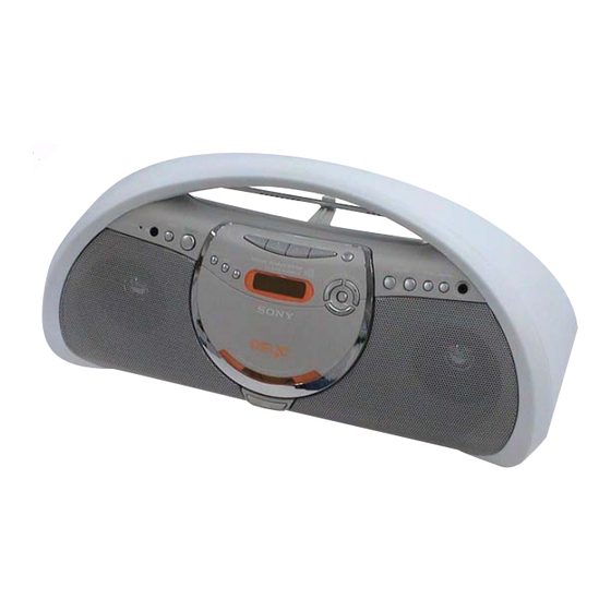
Sony ZS-YN7 Service Manual
Personal audio system
Hide thumbs
Also See for ZS-YN7:
- Operating instructions manual (32 pages) ,
- Operating instructions manual (68 pages) ,
- Brochure & specs (2 pages)
Table of Contents
Advertisement
Quick Links
SERVICE MANUAL
Ver. 1.1 2005.09
US and foreign patents licensed from Dolby Laboratories.
AUDIO POWER SPECIFICATIONS
(US model only)
POWER OUTPUT AND TOTAL HARMONIC
DISTORTION
With 3.2-ohm loads, both channels driven from
100 - 10,000 Hz; rated 1.7 W per channel-
minimum RMS power, with no more than 10 %
total harmonic distortion in AC operation.
Other Specifications
CD player section
System
Compact disc digital audio system
Laser diode properties
Material: GaAlAs
Wave length: 780 nm
Emission duration: Continuous
Laser output: Less than 44.6 µW
(This output is the value measured at a distance of about
200 mm from the objective lens surface on the optical
pick-up block with 7 mm aperture.)
Spindle speed
400 r/min (rpm) to 1 000 r/min (rpm) (CLV)
Number of channels
2
Frequency response
20 - 20 000 Hz +0/–1 dB
Wow and flutter
Below measurable limit
Sony Corporation
9-877-962-02
Personal Audio Group
2005I05-1
Published by Sony Engineering Corporation
© 2005.09
Model Name Using Similar Mechanism
Optical Pick-up Block Name
Optical Pick-up Name
SPECIFICATIONS
Radio section
Frequency range
FM: 87.5 - 108 MHz
AM: 531 - 1 611 kHz (9 kHz step)
530 - 1 610 kHz (10 kHz step)
IF
FM: 10.7 MHz
AM: 450 kHz
Antennas
FM: Telescopic antenna
AM: Built-in ferrite bar antenna
General
Speaker
1
Full range: 8 cm (3
⁄
in.) dia.,
4
3.2 Ω, cone type (2)
Output
Headphones jack (stereo minijack):
For 16 - 64 Ω impedance headphones
Power output
2.3 W + 2.3 W (at 3.2 Ω, 10 % harmonic
distortion)
Power requirements
For player
US, Canadian, E and Mexican models:
120 V AC, 60 Hz
Korean model: 220 V AC, 60 Hz
Singapore and Australian model: 230 V AC, 50 Hz
9 V DC, 6 size C (R14) batteries
For remote control:
3 V DC, 2 size AAA (R03) batteries
Power consumption
16 W
ZS-YN7
Canadian Model
Australian Model
Battery life
For player:
CD playback
Sony R14P: approx. 1.5 h
Sony alkaline LR14: approx. 8 h
Radio reception
Sony R14P: approx. 6 h
Sony alkaline LR14: approx. 20 h
Dimensions
Approx. 455 × 214 × 180 mm (w/h/d)
(18 × 8
× 7
1
⁄
1
⁄
inches) (incl. projecting parts)
2
8
Mass
Approx. 3.5 kg (7 lb. 11 oz) (incl. batteries)
Supplied accessories
AC power cord (1) (US, Canadian, E and Mexican models)
Mains lead (1) (Singapore, Korean and Australian models)
Remote control (1)
CD-ROM (SonicStage) (1)
SonicStage Installation/Operating Guide (1)
Design and specifications are subject to change without
notice.
PERSONAL AUDIO SYSTEM
US Model
E Model
NEW
KSM-213RAP
KSS-213R
Advertisement
Table of Contents

Related Manuals for Sony ZS-YN7


Summary of Contents for Sony ZS-YN7
-
Page 1: Specifications
Sony R14P: approx. 1.5 h 530 - 1 610 kHz (10 kHz step) With 3.2-ohm loads, both channels driven from Sony alkaline LR14: approx. 8 h FM: 10.7 MHz 100 - 10,000 Hz; rated 1.7 W per channel- AM: 450 kHz... -
Page 2: Table Of Contents
PIÈCES SONT CRITIQUES POUR LA SÉCURITÉ DE FONCTIONNEMENT. NE REMPLACER CES COM- POSANTS Earth Ground QUE PAR DES PIÈCES SONY DONT LES NUMÉROS SONT DONNÉS DANS CE MANUEL OU DANS LES SUPPLÉMENTS Fig. A. Using an AC voltmeter to check AC leakage. -
Page 3: Servicing Notes
ZS-YN7 SECTION 1 SERVICING NOTES LASER DIODE AND FOCUS SEARCH OPERATION NOTES ON HANDLING THE OPTICAL PICK-UP CHECK BLOCK OR BASE UNIT During normal operation of the equipment, emission of the laser The laser diode in the optical pick-up block may suffer electrostatic... - Page 4 ZS-YN7 HARNESS SETTING H/P board TU board MAIN board...
-
Page 5: General
ZS-YN7 SECTION 2 This section is extracted from instruction manual. GENERAL Basic Operations Playing a CD Press u (N on the remote). The player plays all the tracks once. Display Audio CD ATRAC CD/MP3 CD* File name Track number Playing time... -
Page 6: Listening To The Radio
ZS-YN7 Listening to the radio Use these buttons for additional operations POWER VOLUME +, – MODE Press If the FM broadcast is adjust the volume VOLUME +*, – (VOL +*, – on the noisy, press MODE until remote) “Mono” appears in the... -
Page 7: Disassembly
ZS-YN7 SECTION 3 DISASSEMBLY • This set can be disassembled in the order shown below. 3-1. DISASSEMBLY FLOW 3-2. CABINET 3-6. LCD BOARD REAR ASSY (Page 10) (Page 8) 3-3. CABINET (UPPER) (Page 8) 3-4. CHASSIS SECTION (Page 9) 3-5. CD BLOCK... -
Page 8: Cabinet Rear Assy
ZS-YN7 Note: Follow the disassembly procedure in the numerical order given. 3 three screws (B2.6) 3-2. CABINET REAR ASSY 4 nine screws (B2.6) 7 cabinet rear assy 2 three screws (B2.6) 6 connector (CN902) 1 battery lid 3-3. CABINET (UPPER) 9 two screws (B2.6) -
Page 9: Shassis Section
ZS-YN7 3-4. CHASSIS SECTION 9 chassis section 8 two screws (B2.6) 5 flexible flat cable (21core) 3 connector 4 TU board (CN803) (CNP1) 8 two screws (B2.6) 6 connector (CN807) 1 screw (B2.6) 3-5. CD BLOCK SECTION 0 four screws 9 spring (CD block) (B2.6) -
Page 10: Lcd Board
ZS-YN7 3-6. LCD BOARD 0 panel CD sub assy 5 CD window qs LCD board qa flexible flat cable (21core) (CN401) 9 five screws (B2.6) 8 KEY (JOG) board 7 flexible flat cable (5core) (CN403) 6 five screws (B2.6) 4 CD ring... -
Page 11: Test Mode
ZS-YN7 SECTION 4 TEST MODE CD TEST MODE Procedure: 1. Press the [POWER] button to turn the power on. 2. Select the CD test mode by momentarily shorting both of TAP (TEST A). Refer to CD section of ELECTRICAL ADJUSTMENT (see page 14) for details of operation in this mode. -
Page 12: Electrical Adjustments
ZS-YN7 SECTION 5 ELECTRICAL ADJUSTMENTS 0 dB=1 µV TUNER SECTION AM IF ADJUSTMENT Adjust for a maximum reading on level meter [AM] 450 kHz Setting: Function: RADIO ( ): Singapore, Korean and Australian models RADIO, AUTO PRESET, BAND button: AM... - Page 13 ZS-YN7 Adjustment and Connecting Location: – TU Board (Component Side) – T2 FM IF Adjustment AM Frequency Coverage Adjustment T1 AM IF Adjustment FM Frequency Coverage Adjustment FM Tracking Adjustment AM Tracking Adjustment – TU Board (Conductor Side) – (ANT)
-
Page 14: Cd Section
ZS-YN7 TRAVERSE CHECK CD SECTION 1. Connect an oscilloscope to TP (TE) and TP (VC) on the CD board. Perform all CD section check in the test mode. 2. Insert the disc (PATD-012). (Part No.: 4-225-203-01) 3. In the STOP2 mode, press the... - Page 15 ZS-YN7 Checking Location: – CD Board (Conductor Side) – (VC) (TE) (RF) IC702 ZS-YN7...
-
Page 16: Diagrams
ZS-YN7 SECTION 6 DIAGRAMS 6-1. BLOCK DIAGRAM – CD SERVO Section – OPTICAL PICK-UP RF AMP, FOCUS/TRACKING BLOCK ERROR AMP CD DSP (KSM-213RAP) IC701 IC702 CD-L RF AC RFAC (Page 18) AOUT1 CD +3.3V RFDC RFDC AOUT2 R-CH RFDCI MP3 DECODER... -
Page 17: Block Diagram - Tuner Section
ZS-YN7 6-2. BLOCK DIAGRAM – TUNER Section – FM IFT FM/AM RF AMP, MIX, OSC, FM IF FM/AM IF AMP, DET, MPX ANT1 FM TELESCOPIC ANTENNA L-OUT TU L-OUT IF-IN RF-IN MIX-OUT FM IF (Page 18) -OUT RF AMP MUTE... -
Page 18: Block Diagram - Main Section
ZS-YN7 6-3. BLOCK DIAGRAM – MAIN Section – • R-ch is omitted due to same as L-ch. R-CH • SIGNAL PATH : FM CD L-OUT (Page 16) CD-L : CD PLAY POWER J321 SELL 2 L-IN IC302 TU L-OUT (Page 17) - Page 19 ZS-YN7 • Note for Printed Wiring Boards and Schematic Diagrams • Circuit Boards Location Note on Printed Wiring Board: Note on Schematic Diagram: • X : parts extracted from the component side. • All capacitors are in µF unless otherwise noted. (p: pF) •...
-
Page 20: Printed Wiring Board - Cd Board
ZS-YN7 • See page 19 for Circuit Boards Location. 6-4. PRINTED WIRING BOARD – CD Board – :Uses unleaded solder. CD BOARD CD BOARD (COMPONENT SIDE) (CONDUCTOR SIDE) C772 OPTICAL C770 PICK-UP C773 BLOCK R791 (KSM-213RAP) C769 M702 IC704 (SPINDLE) -
Page 21: Schematic Diagram - Cd Board
ZS-YN7 • See page 32 for IC Block Diagrams. • See page 31 for Waveforms. • See page 37 for IC Pin Function Description. 6-5. SCHEMATIC DIAGRAM – CD Board – FB712 ON/OFF C748 +1.5V REGULATOR FB704 FB705 FB709 C715... -
Page 22: Printed Wiring Board - Tu Board
ZS-YN7 • See page 19 for Circuit Boards Location. 6-6. PRINTED WIRING BOARD – TU Board – : Uses unleaded solder. ANT1 TELESCOPIC ANTENNA (US, CND, E, MX) JC12 (SP, KR, AUS) (ANT) MAIN BOARD CN303 (Page 25) (US, CND, E, MX) -
Page 23: Schematic Diagram - Tu Board
ZS-YN7 • See page 32 for IC Block Diagrams. • See page 31 for Waveform. 6-7. SCHEMATIC DIAGRAM – TU Board – AM FERRITE-ROD ANTENNA 220p (VT) KV1520NT 100p AM OSC 0.22 0.001 FREQUENCY COVERAGE JC12 JC11 0.01 220k 100p 0.01... -
Page 24: Main Board (Component Side)
ZS-YN7 • See page 19 for Circuit Boards Location. 6-8. PRINTED WIRING BOARD – MAIN Board (Component Side) – : Uses unleaded solder. • Semiconductor Location Ref. No. Location D801 MAIN BOARD (COMPONENT SIDE) D951 D952 IC802 Q951 Q953 IC803... -
Page 25: Main Board (Conductor Side)
ZS-YN7 • See page 19 for Circuit Boards Location. 6-9. PRINTED WIRING BOARD – MAIN Board (Conductor Side) – : Uses unleaded solder. • Semiconductor Location (Page 22) (Page 22) (Page 29) (Page 28) Ref. No. Location TU BOARD TU BOARD... -
Page 26: Schematic Diagram - Main Board (1/2)
ZS-YN7 • See page 32 for IC Block Diagrams. 6-10. SCHEMATIC DIAGRAM – MAIN Board (1/2) – (1/2) R104 R204 R105 R205 R103 R203 2.2k 2.2k C101 R101 C117 1 50V C105 0.001 CN303 C201 R201 C217 1 50V C205 0.001... -
Page 27: Schematic Diagram - Main Board (2/2)
ZS-YN7 6-11. SCHEMATIC DIAGRAM – MAIN Board (2/2) – • See page 31 for Waveform. • See page 37 for IC Pin Function Description. (2/2) CN803 (EXCEPT KR,AUS) Q808 LCD-A0 LCD-A0 DTA114YUA-T106 C840 C456 C455 100p 100p LCD-AD7 LCD-AD7 Q808,809... -
Page 28: Printed Wiring Boards - Key Section
ZS-YN7 • See page 19 for Circuit Boards Location. 6-12. PRINTED WIRING BOARDS – KEY Section – : Uses unleaded solder. (Page 25) KEY (POWER) BOARD KEY (JOG) BOARD MAIN BOARD CN804 S410 S420 R413 R428 REPEAT ROTARY ENCODER CN407... -
Page 29: Printed Wiring Boards - Power Section
ZS-YN7 • See page 19 for Circuit Boards Location. 6-13. PRINTED WIRING BOARDS – POWER Section – : Uses unleaded solder. (Page 25) MAIN BOARD CN904 POWER BOARD BATTERY (R) BOARD 1-862-279- (11) T901 POWER TRANSFORMER DRY BATTERY SIZE "C"... -
Page 30: Schematic Diagram - Key/Power Section
ZS-YN7 6-14. SCHEMATIC DIAGRAM – KEY/POWER Section – CN401 LCD-A0 LCD401 R441 LCD-AD7 RESETB LCD-WR CAP1+ C405 LCD-AD6 R436 R435 CAP1- CN407 100k 470k LCD-CS R403 C417 CAP2+ 0.01 C406 KEY-0B LCD-AD5 CAP2- KEY-0A LCD-RES VOUT LCD-AD4 R401 R402 S402... - Page 31 ZS-YN7 • Waveforms – CD Board – – TU Board – IC701 qg (RFAC) IC703 wl (EXTAL) IC2 w; (XOUT) (CD play mode) (MP3 play mode) 0.9 Vp-p 1.0 Vp-p 0.8 Vp-p 13.3 µ s 44.4 ns 500 mV/DIV, 5 µ s/DIV...
-
Page 32: Ic Block Diagrams
ZS-YN7 • IC Block Diagrams – CD Board – IC701 CXA2647N-T4 ROM/RW DC OFST RFDCI – – RFDC – ROM/RW VOFST APC AMP RF OFF AT VCC RFAC EQ IN ROM/RW RFAC AC SUM SUMMING VOFST – – ROM/RW TE BAL ROM/RW –... - Page 33 ZS-YN7 IC703 CXR710160-209R 64 63 62 61 60 59 58 57 56 55 52 51 50 49 PE3/RxD1 PE2/TxD1 PE1/RxD0 PE0/TxD0 INTERFACE LRCKI BCKI VDIOCD0 PCMDI DVDD4 CD-ROM TEST8 INTERFACE TEST7 DVDD0 DVSS0 DVSS2 VDIO0 DVDD2 VDIOCD1 PC3/SCS0 PF4/XRDE PC2/SI0...
- Page 34 ZS-YN7 IC704 BA5946FP-E2 INTERFACE LEVEL SHIFT MUTE THERNAL SHUTDOWN INTERFACE INTERFACE IC706 S-T111B15MC-OGATFG VOUT ON/OFF OVER CURRENT PROTECTOR ON/OFF REFERENCE CIRCUIT VOLTAGE CIRCUIT...
- Page 35 ZS-YN7 – TU Board – IC1 TA2149BN RF GND FM RFOUT FM RF RF VCC FM RFIN AM RFIN AM LOW CUT MIX OUT FM OSC AM OSC BUFF BUFF 1/1 OR 1/16 OSC OUT LEVEL AM IF AM IF IN...
- Page 36 ZS-YN7 – MAIN Board – IC301 BD3870FS-E2 IC901 S-816A33AMC-BAI-T2 REFERENCE ERROR SINK VOLTAGE DRIVER OVERCURRENT SOURCE PROTECT POWER SUPPLY CIRCUIT...
- Page 37 ZS-YN7 • IC Pin Function Description CD BOARD IC702 CXD3029R (CD DSP) Pin No. Pin Name Description XRAS Row address strobe signal output to the D-RAM Data input enable signal output to the D-RAM 3 to 6 D1, D0, D3, D2...
- Page 38 ZS-YN7 Pin No. Pin Name Description 53, 54 AVSS1, AVSS2 — Ground terminal VREFR R-ch reference voltage output terminal AOUT2 R-ch analog audio signal output terminal AVDD2 — Power supply terminal (+3.3V) TES1 Input terminal for the test (fixed at “L”) TEST Input terminal for the test (fixed at “L”)
- Page 39 ZS-YN7 Pin No. Pin Name Description TRDR Tracking servo drive signal (–) output to the coil/motor drive TFDR Tracking servo drive signal (+) output to the coil/motor drive SRDR Sled servo drive signal (–) output to the coil/motor drive SFDR...
- Page 40 ZS-YN7 MAIN BOARD IC802 TMP91CY22FG-5HF7 (SYSTEM CONTROLLER) Pin No. Pin Name Description VREFL Reference voltage input terminal (0V) AVSS — Ground terminal AVCC — Power supply terminal (+3.3V) RW/ROM CD-ROM/RW or LD on/off selection signal output terminal PWM RF RF offset cancel PWM signal output terminal...
- Page 41 ZS-YN7 Pin No. Pin Name Description 52, 53 JOG-A, JOG-B Jog dial pulse input from the rotary encoder (JOG) Not used TEST A CD test mode setting terminal Normally fixed at “H” TEST B LCD test mode setting terminal Normally fixed at “H”...
-
Page 42: Exploded Views
ZS-YN7 SECTION 7 EXPLODED VIEWS NOTE: • Items marked “*” are not stocked since they • -XX and -X mean standardized parts, so they The components identified by mark 0 or dotted line with mark 0 are may have some difference from the original are seldom required for routine service. -
Page 43: Cabinet Front Section
ZS-YN7 7-2. CABINET FRONT SECTION 66 76 SP101 supplied SP201 not supplied (KEY (OPEN) board) chassis section Ref. No. Part No. Description Remark Ref. No. Part No. Description Remark 3-253-143-01 SCREW (B2.6), (+) P TAPPING 3-040-916-01 FOOT (FRONT), RUBBER 3-265-832-11 HANDLE (FRONT) (EXCEPT US, CND) -
Page 44: Chassis Section
ZS-YN7 7-3. CHASSIS SECTION not supplied Lid CD section 120 139 PL801 optical pick-up block section (KSM-213RAP) Ref. No. Part No. Description Remark Ref. No. Part No. Description Remark 1-829-077-11 CABLE, FLEXIBLE FLAT (29 CORE) A-4547-677-A MAIN BOARD, COMPLETE (KR, AUS) 3-252-828-01 SCREW (B2.6), (+) PWH TAPPING... -
Page 45: Lid Cd Section
ZS-YN7 7-4. LID CD SECTION not supplied LCD401 LCD board Ref. No. Part No. Description Remark Ref. No. Part No. Description Remark 3-253-143-01 SCREW (B2.6), (+) P TAPPING 3-265-860-01 HOLDER, LCD (7) 3-017-951-02 PLATE, CHUCKING X-3385-188-1 CD (7) SUB ASSY, PANEL (US, CND) -
Page 46: Optical Pick-Up Block Section (Ksm-213Rap)
ZS-YN7 7-5. OPTICAL PUCK-UP BLOCK SECTION (KSM-213RAP) not supplied (SPINDLE (M701)) M702 The components identified by Les composants identifiés par une mark 0 or dotted line with marque 0 sont critiques pour la mark 0 are critical for safety. sécurité. -
Page 47: Electrical Parts List
ZS-YN7 BATT (L) SECTION 8 ELECTRICAL PARTS LIST BATT (R) NOTE: • Items marked “*” are not stocked since they • Due to standardization, replacements in the The components identified by mark 0 or dotted line with mark 0 are parts list may be different from the parts are seldom required for routine service. - Page 48 ZS-YN7 Ref. No. Part No. Description Remark Ref. No. Part No. Description Remark C783 1-162-923-11 CERAMIC CHIP 47PF R705 1-216-833-11 METAL CHIP 1/10W C784 1-162-923-11 CERAMIC CHIP 47PF R706 1-216-849-11 METAL CHIP 220K 1/10W C785 1-162-923-11 CERAMIC CHIP 47PF R707...
- Page 49 ZS-YN7 DOOR SW KEY (JOG) Ref. No. Part No. Description Remark Ref. No. Part No. Description Remark R763 1-216-821-11 METAL CHIP 1/10W R764 1-216-853-11 METAL CHIP 470K 1/10W < CONNECTOR > R765 1-216-833-11 METAL CHIP 1/10W R766 1-216-809-11 METAL CHIP...
- Page 50 ZS-YN7 KEY (JOG) KEY (OPEN) KEY (POWER) KEY (VOL) Ref. No. Part No. Description Remark Ref. No. Part No. Description Remark S419 1-786-050-21 SWITCH, KEYBOARD (ENTER/MEMORY) S407 1-786-050-21 SWITCH, KEYBOARD (SOUND) S420 1-476-454-11 ENCODER (ROTARY) (JOG) ************************************************************* ************************************************************* A-4547-646-A LCD BOARD, COMPLETE...
- Page 51 ZS-YN7 MAIN Ref. No. Part No. Description Remark Ref. No. Part No. Description Remark R432 1-216-817-11 METAL CHIP 1/10W C206 1-162-964-11 CERAMIC CHIP 0.001uF R434 1-216-853-11 METAL CHIP 470K 1/10W C207 1-107-826-11 CERAMIC CHIP 0.1uF R435 1-216-853-11 METAL CHIP 470K...
- Page 52 ZS-YN7 MAIN Ref. No. Part No. Description Remark Ref. No. Part No. Description Remark C816 1-162-927-11 CERAMIC CHIP 100PF C959 1-126-176-11 ELECT 220uF C817 1-162-927-11 CERAMIC CHIP 100PF < CONNECTOR > C818 1-162-915-11 CERAMIC CHIP 10PF 0.5PF C819 1-162-915-11 CERAMIC CHIP 10PF 0.5PF...
- Page 53 ZS-YN7 MAIN Ref. No. Part No. Description Remark Ref. No. Part No. Description Remark Q805 8-729-028-99 TRANSISTOR DTC114YUA-T106 Q806 8-729-028-99 TRANSISTOR DTC114YUA-T106 R227 1-216-829-11 METAL CHIP 4.7K 1/10W Q807 8-729-026-53 TRANSISTOR 2SA1576A-T106-QR R230 1-216-864-11 SHORT CHIP Q808 8-729-028-76 TRANSISTOR DTA114YUA-T106...
- Page 54 ZS-YN7 MAIN Ref. No. Part No. Description Remark Ref. No. Part No. Description Remark R490 1-216-821-11 METAL CHIP 1/10W R853 1-216-821-11 METAL CHIP 1/10W R491 1-216-821-11 METAL CHIP 1/10W R854 1-216-833-11 METAL CHIP 1/10W R492 1-216-833-11 METAL CHIP 1/10W R855...
- Page 55 ZS-YN7 MAIN POWER Ref. No. Part No. Description Remark Ref. No. Part No. Description Remark < VARISTOR > 1-164-227-11 CERAMIC CHIP 0.022uF (US, CND, E, MX) VDR801 1-801-862-11 VARISTOR, CHIP (1608) 1-162-970-11 CERAMIC CHIP 0.01uF VDR802 1-801-862-11 VARISTOR, CHIP (1608)
- Page 56 ZS-YN7 Ver. 1.1 Ref. No. Part No. Description Remark Ref. No. Part No. Description Remark < TRIMMER > 1-216-825-11 METAL CHIP 2.2K 1/10W 1-141-442-91 CAP, CERAMIC TRIMMER 1-216-825-11 METAL CHIP 2.2K 1/10W 1-141-304-21 CAP, CERAMIC TRIMMER 1-216-825-11 METAL CHIP 2.2K...
- Page 57 ZS-YN7 Ref. No. Part No. Description Remark Ref. No. Part No. Description Remark 2-023-041-31 MANUAL, INSTRUCTION (ENGLISH, SPANISH) (SP, KR, AUS) 2-023-042-11 MANUAL, INSTRUCTION (SPANISH) (E, MX) 2-023-042-21 MANUAL, INSTRUCTION (KOREAN) (KR) 2-023-043-21 MANUAL (SONIC STAGE2.0) (KR2) (KOREAN) (KR) 3-266-692-11 MANUAL, INSTRUCTION (Sonic Stage Ver. 2.0) (ENGLISH) (US, CND, E, MX) 3-266-692-21 MANUAL, INSTRUCTION (Sonic Stage Ver.
-
Page 58: Revision History
ZS-YN7 REVISION HISTORY Clicking the version allows you to jump to the revised page. Also, clicking the version at the upper right on the revised page allows you to jump to the next revised page. Ver. Date Description of Revision 2004.06...
Need help?
Do you have a question about the ZS-YN7 and is the answer not in the manual?
Questions and answers