Table of Contents
Advertisement
D-190/191/191SR/192CK/193
SERVICE MANUAL
Ver 1.2 1999. 05
with SUPPLEMENT-1
(9-926-937-81)
with SUPPLEMENT-2
(9-926-937-82)
CD player
System
Compact disc digital audio system
Laser diode properties
Material: GaAlAs
Wave length: λ = 780 nm
Emission duration: Continuous
Laser output: Less than 44.6 µW (This output
is the value measured at a distance of 200
mm from the objective lens surface on the
optical pick-up block with 7 mm aperture.)
Error correction
Sony Super Strategy Cross Interleave Reed
Solomon Code
D-A conversion
1-bit quartz time-axis control
Frequency response
20 - 20,000 Hz +1/–3 dB
(measured by EIAJ CP-307)
Output (at 4.5 V input level)
Headphones (stereo minijack)
Approx. 5 mW + approx. 5 mW
at 16 ohms
(Approx. 2 mW + approx. 2 mW
at 16 ohms*)
*For the customers in France
MICROFILM
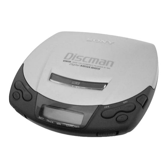
Photo: D-191
Model Name Using Similar Mechanism
CD Mechanism Type
Optical Pick-up Name
SPECIFICATIONS
General
Power requirements
For the area code of the model you purchased,
check the upper left side of the bar code on the
package.
• Sony NC-DMAA rechargeable battery:
2.4 V DC, Ni-Cd, 700 mAh (D-193)
• Two LR6 (size AA) batteries: 3 V DC
• AC power adaptor (DC IN 4.5 V jack):
US/CND/E92/MX model: 120 V, 60 Hz
AEP/FR/EE/E13/G model:
220 - 230 V, 50/60 Hz
UK model: 230 - 240 V, 50 Hz
EA model: 110 - 240 V, 50/60 Hz
AUS model: 240 V, 50 Hz
JEW/E33 model: 100 - 240 V, 50/60 Hz
HK model: 220 V, 50/60 Hz
CH/AR model: 220 V, 50 Hz
• Sony DPM-300P mount plate for use on car
battery: 4.5 V DC
Dimensions (w/h/d) (without projecting parts
and controls)
Approx. 131 × 28 × 148 mm
× 1
× 5
(5
1/4
1/9
Mass (without rechargeable batteries)
Approx. 220 g (7.8 oz.)
Operating temperature
5°C - 35°C (41°F - 95°C)
COMPACT DISC COMPACT PLAYER
– 1 –
US Model
D-191/192CK/193
Canadian Model
AEP Model
UK Model
D-190/191/191SR/192CK/193
Australian Model
D-191/192CK/193
Chinese Model
in.)
4/5
– Continued on next page –
D-191
E Model
D-191/193
NEW
CDM-2811DAA
DAX-11D
Advertisement
Table of Contents

Related Manuals for Sony D-190


Summary of Contents for Sony D-190
- Page 1 HK model: 220 V, 50/60 Hz 20 - 20,000 Hz +1/–3 dB CH/AR model: 220 V, 50 Hz (measured by EIAJ CP-307) • Sony DPM-300P mount plate for use on car Output (at 4.5 V input level) battery: 4.5 V DC Headphones (stereo minijack)
- Page 2 LES COMPOSANTS IDENTIFIÉS PAR UNE MARQUE ! SUR LES DIAGRAMMES SCHÉMATIQUES ET LA LISTE DES PIÈCES SONT CRITIQUES POUR LA SÉCURITÉ DE FONCTIONNEMENT. NE REMPLACER CES COMPOSANTS QUE PAR DES PIÈCES SONY DONT LES NUMÉROS SONT DONNÉS DANS CE MANUEL OU DANS LES SUPPLÉMENTS PUBLIÉS PAR SONY.
-
Page 3: Table Of Contents
TABLE OF CONTENTS 1. SERVICE NOTE 6. EXPLODED VIEWS ..............3 6-1. Cabinet Section ..............20 6-2. MD Section ............... 22 2. GENERAL ................4 7. ELECTRICAL PARTS LIST ......... 23 3. DISASSEMBLY 3-1. Cabinet (Rear) Sub Assy ............. 5 3-2. -
Page 4: General
SECTION 2 GENERAL This section is extracted from instruction manual. – 4 – – 4 –... -
Page 5: Disassembly
SECTION 3 DISASSEMBLY Note : Follow the disassembly procedure in the numerical order given. 3-1. CABINET (REAR) SUB ASSY Note : When installing, fit the knobs (H-B) and switches. 3 claw 1 screws (B2x10) (G), tapping 2 screws (B2x10) (G), tapping 6 cabinet (rear) sub assy 4 claw knob (H-B) -
Page 6: Electrical Adjustments
SECTION 4 ELECTRICAL ADJUSTMENTS CD SECTION CD section adjustments are done automatically in this set. In case of operation check, confirm that focus bias. FOCUS BIAS CHECK 1. Connect the oscilloscope between IC501 pin #¡ (TP552 (RF)) and GND on Main board. 2. -
Page 7: Diagrams
SECTION 5 DIAGRAMS 5-1. IC PIN DESCRIPTION • IC801 CXP401-607R (SYSTEM CONTROL & DIGITAL SIGNAL PROCESSOR) Pin No. Pin Name Pin Description SEIN SENS input from SSP. CNIN Track jump No. count signal input DATO Serial data output to SSP. XLTO Serial data latch output to SSP. - Page 8 Pin No. Pin Name Pin Description SBSO Serial data output of sub P to W. (Not used in this set.) EXCK Serial clock input for SBSO. (Connect to ground in this set.) DTEST LSI test pin (Connect to ground.) CTEST LSI test pin (Connect to ground.) PC0 XSLEEP Power supply IC sleep control output (“L”...
-
Page 9: Block Diagram
D-190/191/191SR/192CK/193 5-2. BLOCK DIAGRAM H/P AMP RF AMP & SYSTEM SERVO PROCESSOR IC301 IC501 AOUT2 RF SUMMING PD1 IV 1 BIT J301 LOUT2 RF O ASYMMETRY DIGITAL EPROM PHONES COLLECTOR DEMODULATOR DIGITAL LOUT1 COLLECTOR PD2 IV FILTER AOUT1 MEGA BASS... -
Page 10: Printed Wiring Board
D-190/191/191SR/192CK/193 5-3. PRINTED WIRING BOARD J401 • Semiconductor DC IN 4.5V ¥ Location Ref. No. Location MAIN BOARD (SIDE A) MAIN BOARD (SIDE B) D301 D401 C-17 D402 B-16 D407 C-13 T401 (OPEN) D408 B-15 DC/DC CONVERTER (D409) (D410) D411... - Page 11 D-190/191/191SR/192CK/193 5-4. SCHEMATIC DIAGRAM — MAIN SECTION (1/2) — • Refer to page 17 for Waveforms and note. • Refer to page 19 for IC Block Diagrams. 700mAh 2.4V (193) – 15 – – 16 –...
-
Page 12: Schematic Diagram -Main Section (1/2)
D-190/191/191SR/192CK/193 5-5. SCHEMATIC DIAGRAM — MAIN SECTION (2/2) — Note: • U : B+ Line. • All capacitors are in µF unless otherwise noted. pF: µµF 50 WV or less are not indicated except for electrolytics • Power voltage is dc 3 V and fed with regulated dc power •... -
Page 13: Ic Block Diagrams
• IC Block Diagrams IC401 SC11252FTAEB DCIN DCIN/VIN VDET VOLTAGE GEN2 RESET CHARGE ERROR CIRCUIT PUMP OUT4B BANDGAP VIN34 VREF REFERENCE OUT3B OUT3A SWITCHING VOUT REGLATER PWM OUTPUT OUT2A CGND MOTOR MOTOR MOTOR MOTOR DRIVER DRIVER DRIVER DRIVER OUT2B – –... -
Page 14: Exploded Views
SECTION 6 EXPLODED VIEWS NOTE: • The mechanical parts with no reference • -XX and -X mean standardized parts, so The components identified by number in the exploded views are not supplied. they may have some difference from the mark ! or dotted line with mark. •... - Page 15 Ref. No. Part No. Description Remark Ref. No. Part No. Description Remark X-4950-609-1 LID ASSY, UPPER (191) (SILVER) 4-214-672-01 HOLDER (LCD) X-4950-610-1 LID ASSY, UPPER (191:CND,AEP,AUS,CH,E13, 4-214-625-11 TERMINAL BOARD (RELAY), BATTERY EE,FR,G,UK/191SR) (BLUE) X-4950-613-1 CABINET (REAR) SUB ASSY X-4950-611-1 LID ASSY, UPPER (191:AEP,AUS,E13,FR,G,UK) 4-966-278-01 FOOT, RUBBER (GREEN) 4-214-668-01 BUTTON (OPEN) (191:US,CND,E92,MX/...
-
Page 16: Md Section
6-2. MD SECTION (CDM-2811DAA) M902 M901 S901 The components identified by Les composants identifiés par une mark ! or dotted line with mark. marque ! sont critiques pour la ! are critical for safety. sécurité. Replace only with part number Ne les remplacer que par une piéce specified. -
Page 17: Electrical Parts List
SECTION 7 MAIN ELECTRICAL PARTS LIST NOTE: • Due to standardization, replacements in • Abbreviation The components identified by the parts list may be different from the : Arabic model mark ! or dotted line with mark. parts specified in the diagrams or the AUS : Australian model ! are critical for safety. - Page 18 MAIN Ref. No. Part No. Description Remark Ref. No. Part No. Description Remark C516 1-104-847-11 TANTAL. CHIP 22uF D412 8-719-404-50 DIODE MA111-TX (193) C517 1-107-826-11 CERAMIC CHIP 0.1uF D413 8-719-037-26 DIODE RD13SB1-T1 C518 1-165-176-11 CERAMIC CHIP 0.047uF D414 8-719-404-50 DIODE MA111-TX C520 1-164-245-11 CERAMIC CHIP 0.015uF...
- Page 19 MAIN Ref. No. Part No. Description Remark Ref. No. Part No. Description Remark < LIQUID CRYSTAL DISPLAY > R309 1-216-845-11 METAL CHIP 100K 1/16W R312 1-216-845-11 METAL CHIP 100K 1/16W LCD801 1-803-508-11 DISPLAY PANEL, LIQUID CRYSTAL R313 1-216-829-11 METAL CHIP 4.7K 1/16W R314...
- Page 20 MAIN Ref. No. Part No. Description Remark Ref. No. Part No. Description Remark R445 1-216-809-11 METAL CHIP 1/16W R622 1-216-841-11 METAL CHIP 1/16W R446 1-216-845-11 METAL CHIP 100K 1/16W R802 1-216-809-11 METAL CHIP 1/16W R501 1-216-793-11 RES,CHIP 1/16W R824 1-218-740-11 METAL CHIP 100K 0.50% 1/16W R502...
- Page 21 Ref. No. Part No. Description Remark Ref. No. Part No. Description Remark ACCESSORIES & PACKING MATERIALS 3-865-739-91 MANUAL, INSTRUCTION (FINNISH) (190:AEP/ 191:AEP/191SR:AEP/192CK:AEP) ******************************** 3-865-741-11 MANUAL, INSTRUCTION 1-251-696-11 CONNECTING PACK, CAR (192CK) (TRADITIONAL CHINESE) (191:E13) 1-467-007-21 ADAPTOR, AC (AC-E455) (AUS) 3-865-741-21 MANUAL, INSTRUCTION (ENGLISH) 1-467-012-11 ADAPTOR, AC (AC-E455) (EA) (191:CH,E13) 1-467-195-11 ADAPTOR, AC (AC-E455A)
- Page 22 D-190/191/191SR/192CK/193 Sony Corporation 99B0490-1 Printed in Japan C1999. 2 9-926-937-11 Personal A&V Products Company Published by Quality Engineering Dept. – 28 – (Shinagawa)
- Page 23 D-191SR Mexican model is almost same as D-191 Mexican model. This Service Manual Supplement-1 contains only the points which differ from D-191 Mexican model. For the informations not contained in this manual, please refer to D-190/191/191SR/192CK/193 service manual (9-926-937-∏) previously issued.
- Page 24 D-190/191/191SR/192CK/193 2. Change of Exploded Views Ref. No. Part No. Description Remark Ref. No. Part No. Description Remark This service manual supplement-2 fully describes the cabinet section shown in the exploded views. X-4950-609-1 LID ASSY, UPPER (SILVER) 4-214-672-01 HOLDER (LCD)
- Page 25 D-190/191/191SR/192CK/193 3. DIAGRAMS • PRINTED WIRING BOARD (SIDE A: TYPE- , SIDE B: TYPE- • Semiconductor J401 DC IN 4.5V Location (-11) ¥ Ref. No. Location D301 MAIN BOARD (SIDE A) MAIN BOARD (SIDE B) D401 C-17 D402 B-16 D407...
- Page 26 D-190/191/191SR/192CK/193 • PRINTED WIRING BOARD (SIDE B: TYPE- J401 DC IN 4.5V ¥ MAIN BOARD (SIDE B) (OPEN) BOARD • DEN BOARD (for TYPE- Ref. No. Part No. Description Remark D404 8-719-158-02 DIODE RD3.9SB2 Q402 8-729-903-10 TRANSISTOR FMW1 R405 1-216-174-00 METAL CHIP...
- Page 27 D-190/191/191SR/192CK/193 • PRINTED WIRING BOARDS (SIDE B: TYPE- J401 DC IN 4.5V ¥ MAIN BOARD (SIDE B) (OPEN) TP413 TP405 D-193 (193) D-193 RECHARGEABLE BATTERY (NICKEL-CADMIUM) NC-DMAA 700mAh 2.4V (190/191/191SR/192CK) DRY BATTERY SIZE " AA " (IEC DESIGNATION R6) 2PCS,3V...
- Page 28 D-190/191/191SR/192CK/193 • PRINTED WIRING BOARDS (SIDE A: TYPE- /IV, SIDE B: TYPE- J401 • Semiconductor DC IN 4.5V ¥ Location (-12) Ref. No. Location MAIN BOARD (SIDE A) MAIN BOARD (SIDE B) D301 D401 C-17 D402 B-16 T401 D404 B-16...
- Page 29 D-190/191/191SR/192CK/193 • PRINTED WIRING BOARD (TYPE- J401 • Semiconductor DC IN 4.5V ¥ Location (-13) Ref. No. Location D301 MAIN BOARD (SIDE A) MAIN BOARD (SIDE B) D401 C-17 D402 B-16 D404 B-16 D407 C-13 T401 (OPEN) DC/DC D408 B-15...
- Page 30 D-190/191/191SR/192CK/193 • PRINTED WIRING BOARD (TYPE- J401 DC IN 4.5V ¥ • Semiconductor Location (-14) MAIN BOARD (SIDE A) MAIN BOARD (SIDE B) Ref. No. Location D301 T401 D401 C-17 DC/DC (OPEN) D402 B-16 CONVERTER D404 B-16 D407 C-13 D408...
- Page 31 D-190/191/191SR/192CK/193 • SCHEMATIC DIAGRAM — MAIN SECTION (1/2) — (TYPE- This note is common for schematic diagrams: • Waveforms • All capacitors are in µF unless otherwise noted. pF: µµF 50 WV or less are not indicated except for electrolytics and tantalums.
- Page 32 D-190/191/191SR/192CK/193 • SCHEMATIC DIAGRAM — MAIN SECTION (1/2) — (TYPE- – 23 – – 24 –...
- Page 33 D-190/191/191SR/192CK/193 • SCHEMATIC DIAGRAM — MAIN SECTION (1/2) — ( TYPE- – 25 – – 26 –...
- Page 34 D-190/191/191SR/192CK/193 • SCHEMATIC DIAGRAM — MAIN SECTION (2/2) — (TYPE- – 27 – – 28 –...
- Page 35 MAIN MAIN 4. ELECTRICAL PARTS LIST NOTE: Ref. No. Part No. Description Remark Ref. No. Part No. Description Remark • Due to standardization, replacements in • Abbreviation The components identified by the parts list may be different from the : Argentina model mark ! or dotted line with mark.
- Page 36 MAIN Ref. No. Part No. Description Remark Ref. No. Part No. Description Remark Q404 8-729-022-67 TRANSISTOR 2SC3650-TD FB201 1-469-121-21 FERRITE, EMI (SMD) (-14) FB201 1-500-444-11 FERRITE, EMI (SMD) (-11/-12-13) Q405 8-729-905-96 TRANSISTOR DTA114TU FB202 1-500-444-11 FERRITE, EMI (SMD) Q406 8-729-922-34 TRANSISTOR 2SD1758-TLQR (193) FB301 1-469-121-21 FERRITE, EMI (SMD) (-14) Q407...
- Page 37 MAIN Ref. No. Part No. Description Remark Ref. No. Part No. Description Remark R406 1-216-174-00 METAL CHIP 1/8W R448 1-216-801-11 METAL CHIP 1/16W (-14) (-12/-13/-14) R406 1-216-813-11 METAL CHIP 1/16W R449 1-216-864-11 METAL CHIP 1/16W (-12/-13) (-12/-13/-14) R408 1-216-843-11 METAL CHIP 1/16W R451 1-216-829-11 METAL CHIP...
- Page 38 MAIN Ref. No. Part No. Description Remark Ref. No. Part No. Description Remark R548 1-216-864-11 METAL CHIP 1/16W ACCESSORIES & PACKING MATERIALS (-12/-13/-14) ******************************** R549 1-216-855-11 METAL CHIP 680K 1/16W (-14) 1-251-696-11 CONNECTING PACK, CAR (192CK:US,E92) R601 1-216-845-11 METAL CHIP 100K 1/16W 1-467-007-21 ADAPTOR, AC (AC-E455)
- Page 39 D-190/191/191SR/192CK/193 MAIN Ref. No. Part No. Description Remark Ref. No. Part No. Description Remark 3-865-739-41 MANUAL, INSTRUCTION (DUTCH) (190:AEP/ 3-867-368-41 MANUAL, INSTRUCTION (PORTUGUESE) 191:AEP,EE/191SR:AEP,EE/192CK:AEP,EE) (191:E92/192CK:E92) 3-865-739-51 MANUAL, INSTRUCTION (SWEDISH) 3-867-369-11 MANUAL, INSTRUCTION (SPANISH) (190:AEP/191:AEP/191SR:AEP/192CK:AEP) (192CK:E92) 3-865-739-61 MANUAL, INSTRUCTION (PORTUGUESE) 3-867-369-21 MANUAL, INSTRUCTION (ENGLISH)
Need help?
Do you have a question about the D-190 and is the answer not in the manual?
Questions and answers