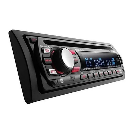
Sony CDX-GT414U Service Manual
Fm/mw/lw compact disc player
Hide thumbs
Also See for CDX-GT414U:
- Operating instructions manual (112 pages) ,
- Installation/connections (2 pages)
Table of Contents
Advertisement
CDX-GT410U/GT414U
SERVICE MANUAL
Ver. 1.1 2007.03
• The tuner and CD sections have no adjustments.
CD player section
Signal-to-noise ratio
120 dB
Frequency response
10 – 20,000 Hz
Wow and flutter
Below measurable limit
Tuner section
FM
Tuning range
87.5 – 108 MHz
Antenna terminal
External antenna connector
Intermediate frequency 10.7 MHz/450 kHz
Usable sensitivity
9 dBf
Selectivity
75 dB at 400 kHz
Signal-to-noise ratio
67 dB (stereo), 69 dB (mono)
Harmonic distortion at 1 kHz
0.5% (stereo), 0.3% (mono)
Separation
35 dB at 1 kHz
Frequency response
30 – 15,000 Hz
Sony Corporation
9-887-452-02
eVehicle Division
2007C04-1
Published by Sony Techno Create Corporation
© 2007.03
(Photo: CDX-GT410U)
Model Name Using Similar Mechanism
CD Drive Mechanism Type
Optical Pick-up Name
SPECIFICATIONS
MW/LW
Tuning range
Antenna terminal
Intermediate frequency 10.7 MHz/450 kHz
Sensitivity
USB player section
Interface
Maximum current
Power amplifier section
Outputs
Speaker impedance
Maximum power output
FM/MW/LW COMPACT DISC PLAYER
AEP Model
UK Model
NEW
MG-101U-188//Q
DAX-25A
MW: 531 – 1,602 kHz
LW: 153 – 279 kHz
External antenna connector
MW: 30 µV, LW: 40 µV
USB (Full-speed)
500 mA
Speaker outputs (sure seal connectors)
4 – 8 ohms
50 W × 4 (at 4 ohms)
– Continued on next page –
Advertisement
Table of Contents

Related Manuals for Sony CDX-GT414U


Summary of Contents for Sony CDX-GT414U
- Page 1 50 W × 4 (at 4 ohms) Separation 35 dB at 1 kHz Frequency response 30 – 15,000 Hz – Continued on next page – FM/MW/LW COMPACT DISC PLAYER Sony Corporation 9-887-452-02 eVehicle Division 2007C04-1 Published by Sony Techno Create Corporation © 2007.03...
- Page 2 COMPONENTS IDENTIFIED BY MARK 0 OR DOTTED LINE WITH MARK 0 ON THE SCHEMATIC DIAGRAMS AND IN THE PARTS LIST ARE CRITICAL TO SAFE OPERATION. REPLACE THESE COMPONENTS WITH SONY PARTS WHOSE PART NUMBERS APPEAR AS SHOWN IN THIS MANUAL OR IN SUPPLEMENTS PUBLISHED BY SONY.
- Page 3 CDX-GT410U/GT414U • This compact disc player is classified as a CLASS 1 LASER UNLEADED SOLDER product. The CLASS 1 LASER PRODUCT label is located on the Boards requiring use of unleaded solder are printed with the lead- exterior. free mark (LF) indicating the solder contains no lead. (Caution: Some printed circuit boards may not come printed with the lead free mark due to their particular size.) : LEAD FREE MARK...
-
Page 4: Table Of Contents
CDX-GT410U/GT414U Ver. 1.1 NOTE FOR REPLACEMENT OF THE SERVO BOARD TABLE OF CONTENTS When repairing, the complete SERVO board (A-1177-201-A) should be replaced since any parts in the SERVO board cannot be repaired. GENERAL Location of Controls ............5 Connections ..............6 NOTE FOR REPLACEMENT OF THE USB CONNECTOR (CN902) DISASSEMBLY... -
Page 5: General
DSPL AF/TA To attenuate the sound. To cancel, press M MODE button 8, 13 again. To select the radio band (FM/MW/LW); CDX-GT414U ws SEL (select) button select the unit* ; select the play mode* qfqg CDX-GT410U The same as the select button on the unit. -
Page 6: Connections
CDX-GT410U/GT414U • CONNECTIONS Connection example Notes (2- A ) • Be sure to connect the ground (earth) lead before connecting the amplifi er. • The alarm will only sound if the built-in amplifi er is used. Tip (2- B - ) For connecting two or more CD/MD changers, the source selector XA-C40 (not supplied) is necessary. - Page 7 CDX-GT410U/GT414U Supplied with XA-C40 Note for the antenna (aerial) connecting Remarque sur le raccordement de Opmerking bij de antenne-aansluiting If your car antenna (aerial) is an l’antenne Indien uw auto is uitgerust met een Mit dem XA-C40 geliefert ISO (International Organization for Si votre antenne de voiture est de type antenne van het type ISO (International Fourni avec le XA-C40...
-
Page 8: Disassembly
CDX-GT410U/GT414U Ver. 1.1 SECTION 2 DISASSEMBLY Note: This set can be disassemble according to the following sequence. 2-1. SUB PANEL (FL-U) ASSY (Page 9) 2-2. CD MECHANISM BLOCK (Page 9) 2-4. SERVO BOARD 2-3. MAIN BOARD (Page 10) (Page 10) 2-5. -
Page 9: Sub Panel (Fl) Assy
CDX-GT410U/GT414U Note: Follow the disassembly procedure in the numerical order given. 2-1. SUB PANEL (FL) ASSY 3 two claws 2 two claws 1 two screws (+PTT 2.6 × 6) 4 sub panel (FL-U) assy 2-2. CD MECHANISM BLOCK 7 bracket (CD) 8 CD mechanism block 6 two screws (+PTT 2.6 ×... -
Page 10: Main Board
CDX-GT410U/GT414U 2-3. MAIN BOARD 2 two screws 4 two screws (+PTT 2.6 × 8) (+PTT 2.6 × 10) 5 two screws (+P 2.6 × 8) 1 three screws 6 two screws (+BTT 2.6 × 5) (+PTT 2.6 × 10) 7 screw (+P 2.6 ×... -
Page 11: Chassis (T) Sub Assy
CDX-GT410U/GT414U 2-5. CHASSIS (T) SUB ASSY 2 two precision screws 1 two precision screws (+P 1.7 × 2.2) (+P 1.7 × 2.2) 4 chassis (T) sub assy 3 claw 2-6. ROLLER ARM ASSY 5 roller arm assy 4 gear (RA1) 1 spring (RAL) 3 washer 2 spring (RAR) -
Page 12: Chassis (Op) Assy
CDX-GT410U/GT414U Ver. 1.1 2-7. CHASSIS (OP) ASSY 6 chassis (OP) assy 1 tension spring (KF) 7 coil spring (damper) (natural) 8 coil spring (damper) (green) 4 slider (R) 3 lever (D) 2 gear (LE1) -
Page 13: Diagnosis Function
CDX-GT410U/GT414U SECTION 3 DIAGNOSIS FUNCTION Description of the Diagnostics function: 4. Contents of each display mode 4-1. Reset count display mode 1. Setting the Diag display mode With the power off, press the [4] button, [5] button, and [4] button on the set body or the remote control (for more than 2 seconds) in turn. - Page 14 CDX-GT410U/GT414U 4-5. CD error information display mode 4-6. OFFSET/FAILURE error display mode 4-5-1. Error description 0 6 1 X X X X X 0 5 1 Operating hours Error information Error description Error description Indication Description (in hexadecimal (0: OFFSET, 1: FAILURE) SERVO ERROR format) Recency of information...
- Page 15 CDX-GT410U/GT414U 4-7-2. Disc type and operating hours The display mode is switched by each rotation of [2/GP/ALBM+] or [1/GP/ALBM--] keys during the CD error information display mode. 0 7 1 X X X X Operating hours USB error info history 1 (latest) Error description plus error details display Recency of information 1-5: 1 represents the latest.
- Page 16 CDX-GT410U/GT414U MEMO...
-
Page 17: Diagrams
CDX-GT410U/GT414U SECTION 4 DIAGRAMS 4-1. BLOCK DIAGRAM — MAIN SECTION — J652 (1/2) ELECTRONIC VOLUME AUDIO IC401 BUS-RCH J652 (2/2) 2 BUS-LCH SUBOUT-L BUS-RCH 1 BUS-RCH AUDIO OUT SUBOUT-R R-CH REAR/SUB CD L 6 CD-LCH R-CH MUTE CD R CD-RCH CD-RCH 5 CD-RCH Q432... -
Page 18: Block Diagram -Display Section
CDX-GT410U/GT414U 4-2. BLOCK DIAGRAM — DISPLAY SECTION — FL901 FLUORESCENT SYSTEM CONTROL INDICATOR TUBE IC501 (2/2) GRID1 KEYIN0 KEY MATRIX GRID2 LSW901,902 FL SO S901–904,906–915 KEYIN1 FL SCK GRID3 FL CS D503 FL DRIVE • FL VH+12V KEY ACKNOWLEDGE Q883 SWITCH KEYACK Q664... - Page 19 CDX-GT410U/GT414U • NOTE FOR PRINTED WIRING BOARDS AND SCHEMATIC DIAGRAMS • Waveforms — MAIN Board — THIS NOTE IS COMMON FOR PRINTED WIRING BOARDS AND SCHEMATIC DIAGRAMS. (In addition to this, the necessary note is IC501 i; (XOUT) printed in each block.) For schematic diagrams.
-
Page 20: Printed Wiring Board -Main Section
CDX-GT410U/GT414U 4-3. PRINTED WIRING BOARD — MAIN SECTION — : Uses unleaded solder. J652 CNJ400 (BUS CONTROL IN) CN300 CNJ400 C330 C325 JW50 R450 R449 C443 C445 JW51 F901 C307 C305 C304 C301 C413 C452 C423 C426 C414 C432 IC300 R301 R447 R448... -
Page 21: Schematic Diagram -Main Section (1/3)
CDX-GT410U/GT414U 4-4. SCHEMATIC DIAGRAM — MAIN SECTION (1/3) — • Refer to page 26 for IC Block Diagrams. C303 C302 JC939 L902 C325 C444 C424 C330 JC940 C306 JC29 JC30 C308 L901 JC31 C309 C301 C304 IC B/D C305 C307 C317 IC300 R301... -
Page 22: Schematic Diagram -Main Section (2/3)
CDX-GT410U/GT414U • Refer to page 19 for Waveforms. 4-5. SCHEMATIC DIAGRAM — MAIN SECTION (2/3) — • Refer to page 26 for IC Block Diagrams. J652 C452 C432 C413 C414 C445 C443 JC942 JC941 C426 C423 JC943 C463 C462 JC10 Q470 Q460 Q420... -
Page 23: Schematic Diagram -Main Section (3/3)
CDX-GT410U/GT414U • Refer to page 19 for Waveforms. • Refer to page 27 for IC Block Diagrams. 4-6. SCHEMATIC DIAGRAM — MAIN SECTION (3/3) — • Refer to page 28 for IC Pin Description of IC501. (Page 21) (Page 22) CN351 JC902 JC901... -
Page 24: Printed Wiring Board -Key Section
CDX-GT410U/GT414U 4-7. PRINTED WIRING BOARD — KEY SECTION — : Uses unleaded solder. LED843 LED841 LED943 LED941 S902 S901 R903 R904 LED842 R943 LED942 LED961 S903 LSW902 LSW901 R947 R847 R906 R907 R908 LED864 S907 C974 R977 R909 R853 S908 S909 S910 S911... -
Page 25: Schematic Diagram -Key Section
CDX-GT410U/GT414U 4-8. SCHEMATIC DIAGRAM — KEY SECTION — R975 R978 R941 R841 LED946 LED846 R949 R849 R953 R853 LED861 IC972 R976 R943 R843 R947 R847 R951 R851 LED961 LED863 R977 R981 IC971 R942 R842 R945 R845 LED950 LED850 LED957 LED857 R861 C976 LED944... - Page 26 CDX-GT410U/GT414U • IC BLOCK DIAGRAMS IC300 TDA8588AJ/N2/R1/M5 (AEP, UK MODEL) (MAIN Board (1/3)) IC601 BA8271F-E2 (MAIN Board (1/3)) IC300 TDA8588AJ/N2/R1 (RUSSIA MODEL) (MAIN Board (1/3)) BUS ON BUS ON SWITCH OUT-FL- RESET C BUS RESET SWITCH BUS ON CLK IN OUT-FL+ BATTERY BATT...
- Page 27 CDX-GT410U/GT414U IC50 TDA7333013TR (MAIN Board (2/3)) BAND PASS SINC4 SIGMA DELTA INTERPOLATOR FILTER FILTER CONVERTER VDDA INTN REF3 SDAOUT REF2 SDAIN RDSREG TEST LOGIC BUFFER SA_DATAOUT REF1 INTN C/SPI DEMODULATOR & & & INTERFACE SYNCHRONIZATION SDA_DATAIN CONTROL PIN MUX'S TESTREG SCL_CLK LOGIC OSCILLATOR...
- Page 28 CDX-GT410U/GT414U IC803 BD9778HFP (MAIN Board (3/3)) DRIVER RESET LATCH CURRENT LIMIT VREF COMPARATOR ERROR SOFT VREF START ON/OFF L:OFF H:ON...
- Page 29 CDX-GT410U/GT414U • IC PIN DESCRIPTION IC501 MB90F046PF-G-101E1 (SYSTEM CONTROL) (MAIN BOARD (3/3)) Pin No. Pin Name Pin Description AREASEL0 Destination setting pin 0 AREASEL1 Destination setting pin 1 AREASEL2 Destination setting pin 2 B-OUTSEL Black-out with/without discrimination signal input “H”: Black-out DIAG Status signal input from power amplifier AAC SEL...
- Page 30 Pin Description Not used. (Open) DAVN RDS (Radio Data System) data block synchronized detect signal input Not used. (Open) UNISI SONY bus data signal input UNISO SONY bus data signal output UNISCK SONY bus clock signal output Z MUTE Mute signal input...
-
Page 31: Exploded Views
CDX-GT410U/GT414U SECTION 5 EXPLODED VIEWS NOTE: • The mechanical parts with no reference • -XX and -X mean standardized parts, so The components identified by mark 0 or dotted line with mark number in the exploded views are not supplied. they may have some difference from the 0 are critical for safety. -
Page 32: Front Panel Section
A-1226-240-A PANEL COMPLETE ASSY, FRONT (GT410U:RU) 2-686-941-01 HOLDER (USB) A-1228-536-A PANEL COMPLETE ASSY, FRONT (GT414U:RU) X-2149-754-1 BUTTON ASSY (S) (GT410U) 2-686-945-01 CAP (USB) 3-251-320-01 EMBLEM (NO. 2.5), SONY X-2149-755-1 BUTTON ASSY (S) (GT414U) CN902 1-820-877-11 CONNECTOR, USB (SOCKET) (USB) X-2149-758-1 PANEL (SV) ASSY, FRONT (GT410U) -
Page 33: Cd Mechanism Section (Mg-101U-188//Q)
CDX-GT410U/GT414U Ver. 1.1 5-3. CD MECHANISM SECTION (MG-101U-188//Q) NOTE: Refer to SUPPLEMENT-1 for disassembly of OPTICAL PICK-UP. not supplied not supplied not supplied not supplied not supplied not supplied not supplied not supplied not supplied not supplied not supplied not supplied Ref. -
Page 34: Electrical Parts List
CDX-GT410U/GT414U SECTION 6 ELECTRICAL PARTS LIST NOTE: • Due to standardization, replacements in • Items marked “*” are not stocked since The components identified by mark 0 or dotted line with mark the parts list may be different from the they are seldom required for routine service. - Page 35 CDX-GT410U/GT414U Ref. No. Part No. Description Remark Ref. No. Part No. Description Remark LED957 8-719-053-09 LED SML-310VTT86 (AF/TA) R910 1-216-823-11 METAL CHIP 1.5K 1/10W LED961 8-719-053-09 LED SML-310VTT86 (RING ILLUMINATION) R911 1-216-824-11 METAL CHIP 1.8K 1/10W LED962 8-719-053-09 LED SML-310VTT86 (RING ILLUMINATION) R912 1-216-825-11 METAL CHIP 2.2K...
- Page 36 CDX-GT410U/GT414U MAIN Ref. No. Part No. Description Remark Ref. No. Part No. Description Remark S913 1-786-653-21 SWITCH, TACTILE (5) C362 1-127-715-11 CERAMIC CHIP 0.22uF S914 1-786-653-21 SWITCH, TACTILE (6/PAUSE) C363 1-126-160-11 ELECT S915 1-786-653-21 SWITCH, TACTILE (AF/TA) C364 1-126-160-11 ELECT C365 1-126-960-11 ELECT *************************************************************...
- Page 37 CDX-GT410U/GT414U MAIN Ref. No. Part No. Description Remark Ref. No. Part No. Description Remark C600 1-126-935-11 ELECT 470uF D106 8-719-977-12 DIODE DTZ6.8B C601 1-162-970-11 CERAMIC CHIP 0.01uF D107 8-719-977-12 DIODE DTZ6.8B C622 1-126-924-11 ELECT 330uF D108 8-719-977-12 DIODE DTZ6.8B C623 1-126-916-11 ELECT 1000uF 6.3V...
- Page 38 CDX-GT410U/GT414U MAIN Ref. No. Part No. Description Remark Ref. No. Part No. Description Remark < JACK > JC929 1-216-296-11 SHORT CHIP JC930 1-216-864-11 SHORT CHIP 1-815-185-13 JACK (ANTENNA) JC931 1-216-864-11 SHORT CHIP J652 1-774-699-12 JACK, PIN 4P (BUS AUDIO IN, JC932 1-216-864-11 SHORT CHIP AUDIO OUT REAR/SUB)
- Page 39 CDX-GT410U/GT414U MAIN Ref. No. Part No. Description Remark Ref. No. Part No. Description Remark Q664 8-729-027-23 TRANSISTOR DTA114EKA-T146 R450 1-216-833-11 METAL CHIP 1/10W Q701 8-729-120-28 TRANSISTOR 2SC1623-L5L6 R451 1-216-809-11 METAL CHIP 1/10W Q702 8-729-120-28 TRANSISTOR 2SC1623-L5L6 R452 1-216-809-11 METAL CHIP 1/10W Q805 8-729-027-43 TRANSISTOR DTC114EKA-T146...
- Page 40 CDX-GT410U/GT414U MAIN SERVO Ref. No. Part No. Description Remark Ref. No. Part No. Description Remark R599 1-216-864-11 SHORT CHIP R924 1-216-845-11 METAL CHIP 100K 1/10W R600 1-216-845-11 METAL CHIP 100K 1/10W R925 1-216-864-11 SHORT CHIP R601 1-216-851-11 METAL CHIP 330K 1/10W R926 1-216-864-11 SHORT CHIP...
- Page 41 CDX-GT410U/GT414U Ref. No. Part No. Description Remark PARTS FOR INSTALLATION AND CONNECTIONS *************************************** X-3382-647-1 FRAME ASSY, FITTING 2-686-803-01 COLLAR 3-246-471-01 KEY (FRAME) X-3382-926-1 SCREW ASSY (BS), FITTING 3-349-410-11 BUSHING 1-465-459-31 ADAPTOR, ANTENNA 1-831-838-11 CORD (WITH CONNECTOR) (ISO) (POWER) × 2...
- Page 42 CDX-GT410U/GT414U MEMO...
-
Page 43: Revision History
CDX-GT410U/GT414U REVISION HISTORY Clicking the version allows you to jump to the revised page. Also, clicking the version at the upper on the revised page allows you to jump to the next revised page. Ver. Date Description of Revision 2006.10 2007.03 Notes for removal of the OPTICAL PICK-UP added.
Need help?
Do you have a question about the CDX-GT414U and is the answer not in the manual?
Questions and answers