Table of Contents
Advertisement
Quick Links
Download this manual
See also:
Instruction Manual
Advertisement
Table of Contents

Related Manuals for Icom IC-M32


Summary of Contents for Icom IC-M32
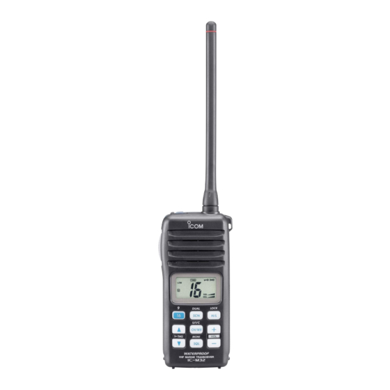
- Page 1 VHF MARINE TRANSCEIVER iC-m32...
- Page 2 INTRODUCTION This service manual describes the latest service information for the IC-M32 VHF MARINE TRANSCEIVER at the time of publication. To upgrade quality, all electrical or mechanical parts and internal circuits are subject to change without notice or oblig- ation.
-
Page 3: Table Of Contents
TABLE OF CONTENTS SECTION SPECIFICATIONS SECTION INSIDE VIEWS SECTION DISASSEMBLY INSTRUCTIONS SECTION CIRCUIT DESCRIPTION RECEIVER CIRCUITS ........... . .4-1 TRANSMITTER CIRCUITS . - Page 4 SECTION 1 SPECIFICATIONS ‘ ‘ GENERAL • Frequency coverage : 156.025–157.425 MHz 156.050–163.275 MHz • Type of emission : 16K0G3E : 50 Ω • Antenna impedance • MIC impedance : 2 kΩ : 8 Ω • Audio impedance • Power supply requirement : 7.2 V DC (negative ground;...
-
Page 5: Vhf Marine Channel List
‘ ‘ VHF MARINE CHANNEL LIST Channel No. Frequency (MHz) Channel No. Frequency (MHz) Channel No. Frequency (MHz) Transmit Receive Transmit Receive Transmit Receive 156.050 160.650 157.050 157.050 156.675 156.675 156.050 156.050 157.100 161.700 156.725 156.725 156.100 160.700 157.100 157.100 156.875 156.875 156.150... - Page 6 SECTION 2 INSIDE VIEWS • MAIN UNIT TOP VIEW BOTTOM VIEW Antenna switching circuit (D52: MA77) Antenna switching circuit (D90: 1SV307) (IC50: NJM2125F) Power amplifier (Q54: RD07MVS1) 1st mixer (Q150: 3SK299) IF amplifier IF detector IC (Q151: 2SC2714 Y) (IC170: TA31136FN) TX/RX switch (D50, D51: MA77) VCO circuit...
-
Page 7: Section 3 Disassembly Instructions
A : For IC-M2A only. ¡ ¡ Removing the MAIN unit B : For IC-M32 only. NOTE: The chassis panel MP31 is a common parts for IC-M2A and IC-M32. Need to screw the MP42 (C) to the B location for IC-M32. MAIN unit Chassis MP31 q Unscrew 7 screws, H (2 ×... -
Page 8: Section 4 Circuit Description
SECTION 4 CIRCUIT DESCRIPTION 4-1 RECEIVER CIRCUITS 4-1-3 2ND IF AND DEMODULATOR CIRCUITS (MAIN UNIT) 4-1-1 ANTENNA SWITCHING CIRCUIT The 2nd mixer circuit converts the 1st IF signal to a 2nd IF (MAIN UNIT) signal. A double conversion superheterodyne system (which The antenna switching circuit functions as a low-pass filter converts receive signal twice) improves the image rejection while receiving and as resonator circuit while transmitting. -
Page 9: Transmitter Circuits
4-1-5 SQUELCH CIRCUIT (MAIN UNIT) 4-2-3 DRIVE/POWER AMPLIFIER CIRCUITS The noise squelch circuit cuts out AF signals when no RF (MAIN UNIT) signals are received. By detecting noise components in the The signal from the VCO circuit passes through the trans- AF signals, the squelch circuit switches the AF mute switch. -
Page 10: Pll Circuit
4-4 POWER SUPPLY CIRCUITS 4-3 PLL CIRCUIT (MAIN UNIT) VOLTAGE LINES A PLL circuit provides stable oscillation of the transmit fre- quency and receive 1st LO frequency. The PLL output com- LINE DESCRIPTION pares the phase of the divided VCO frequency to the refer- The voltage from the attached battery pack. -
Page 11: Port Allocations
4-5 PORT ALLOCATIONS 4-5-1 CPU (IC360) Port Port Description Description number name number name Input port for the [CH/WX] key. Input port for the RSSI signal to con- CH/WX RSSIV trol S-meter from the FM IF IC (IC170 Low : While [CH/WX] key is pushed. pin 12). -
Page 12: Section 5 Adjustment Procedures
SECTION 5 ADJUSTMENT PROCEDURES 5-1 PREPARATION When adjusting IC-M32, the optional CS-M32 (Rev. 1.0 or later), OPC-478 are required. CLONING SOFTWARE CLONING CABLE EQUIPMENT GRADE AND RANGE EQUIPMENT GRADE AND RANGE Output voltage : 7.5 V DC Frequency range : 30–300 MHz... - Page 13 • CONNECTION Standard signal generator to the antenna connector CAUTION! 0.1 V to 32 mV ( 127 dBm to 17 dBm) DO NOT transmit while an SSG is connected to the antenna connector. Attenuator to [MIC] jack Audio generator FM deviation meter 40 dB or 50 dB RF power meter to [SP] jack...
- Page 14 5-2 PLL AND RX SENSITIVITY ADJUSTMENTS ADJUSTMENT MEASUREMENT POINT ADJUSTMENT ADJUSTMENT CONDITION VALUE UNIT LOCATION UNIT ADJUST LOCK • Operating frq. : 156.800 MHz MAIN Connect a digital 1.8 V Verify VOLTAGE • Receiving multi-meter or oscil- loscope check point CP1. •...
- Page 15 5-3 ADJUSTMENT MODE ADJUSTMENTS Select an operation using [16] key, then set specified value using [Y] / [Z] keys on the front panel of IC-M32. MEASUREMENT ADJUSTMENT ADJUSTMENT CONDITION VALUE UNIT LOCATION REFERENCE • Operating frq. :156.800 MHz Loosely couple the frequency 156.8000 MHz...
-
Page 16: Parts List
SECTION 6 PARTS LIST [MAIN UNIT] [MAIN UNIT] ORDER ORDER DESCRIPTION DESCRIPTION 1130007610 S.IC µPD3140GS-E1 (DS8) 6200003710 S.COIL NL 252018T-2R7J IC50 1120002830 S.IC NJM2125F-TE1 6200008280 S.COIL 0.30-1.7-7TL 50N IC170 1110003200 S.IC TA31136FN (EL) 6200009800 S.COIL 0.26-1.1-7TR 30N IC190 1190000350 S.IC M62363FP-650C 6200008580 S.COIL... - Page 17 [MAIN UNIT] [MAIN UNIT] ORDER ORDER DESCRIPTION DESCRIPTION ERJ3GEYJ 121 V (120 Ω) R134 7030003330 S.RESISTOR R351 7030003440 S.RESISTOR ERJ3GEYJ 102 V (1 kΩ) ERJ3GEYJ 101 V (100 Ω) R150 7030003320 S.RESISTOR R352 7030003580 S.RESISTOR ERJ3GEYJ 153 V (15 kΩ) R151 7030003500 S.RESISTOR...
- Page 18 [MAIN UNIT] [MAIN UNIT] ORDER ORDER DESCRIPTION DESCRIPTION 4030007050 S.CERAMIC C1608 CH 1H 220J-T C228 4030017460 S.CERAMIC ECJ0EB1E102K 4030006860 S.CERAMIC C1608 JB 1H 102K-T C229 4030017460 S.CERAMIC ECJ0EB1E102K 4030007040 S.CERAMIC C1608 CH 1H 180J-T C230 4550006820 S.TANTALUM ECST1DX106R 4030007040 S.CERAMIC C1608 CH 1H 180J-T C231 4030008680...
- Page 19 [CHASSIS UNIT] ORDER DESCRIPTION 6910014190 CONNECTOR 2497 ANT CONNECTOR 2510001092 SPEAKER 036D0801B <FG> 8900010960 CABLE OPC-1129 M.=Mounted side (T: Mounted on the Top side, B: Mounted on the Bottom side) S.=Surface mount 6 - 4...
- Page 20 SECTION 7 MECHANICAL PARTS AND DISASSEMBLY [CHASSIS PARTS] [ACCESSORIES] ORDER ORDER QTY. QTY. DESCRIPTION DESCRIPTION 6910014190 2497 ANT connector 3310002321 Antenna FA-SC55V-1 Optional products Charger BM-95V [AUS] Optional products Charger BC-147A [USA] SP 1 2510001092 Speaker 036D0801B <FG> Optional products Charger BC-147E [SEA] Optional products...
- Page 21 MP24 (C) Screw ....MP25 (C) Sealing washer NOTE: The MP31 (C) is a common parts for IC-M2A and IC-M32. Need to screw the MP42 (C) to the B location for IC-M32.
- Page 22 ¢ ¢ BC-150 CHARGER PARTS LIST ¡ ¡ ELECTRICAL PARTS [CHARGE UNIT] REF. NO. ORDER NO. DESCRIPTION MP1(C) 7070001130 RESISTOR 120 ERG2SJ 7070001140 RESISTOR 150 ERG2SJ 7010007100 RESISTOR 1K PSD1/4V 6510023070 CONNECTOR HEC2305-01-250 5040001390 LED TLG124A 0910054642 PCB B-5787B ¡ ¡ MECHANICAL PARTS [CHASSIS] REF.
- Page 23 SECTION 8 SEMI-CONDUCTOR INFORMATION SECTION PARTS LIST • TRANSISTOR AND FET’S 2SA1588 GR 2SB1132 Q 2SC2714 Y 2SC4213 B 2SC4215 O (Symbol: ZG) (Symbol: BAQ) (Symbol: QY) (Symbol: AB) (Symbol: QO) 2SC4226 R25 DTA144 EUA DTC144 TU 3SK299 U73 UN911 H (Symbol: R25) (Symbol: U73) (Symbol: 16)
- Page 24 SECTION 9 BOARD LAYOUTS The combination of this page and the next page shows MAIN UNIT the unit layout in the same configuration as the actual • TOP VIEW P.C. Board. + – CLONE MONI U/I/C DUAL CH/WX DS246 AFOUT LOCK –...
- Page 25 The combination of this page and the previous page • BOTTOM VIEW shows the unit layout in the same configuration as the actual P.C. Board. MC250 – CLONE J250 AFOUT 9 - 2...
- Page 26 SECTION 10 BLOCK DIAGRAM CHASSIS MAIN UNIT ANTENNA REF OSC D50, D51: D52, D90: Q21, Q22: 2SC4226 Q23: Q24: Q50: Q53: Q54: 21.250 MHz MA77 1SV307 D22, D23: HVU350B 2SC4215 2SC4215 2SC4226 RD01MUS1 RD07MVS1 PLL IC LOOP TX/RX BUFF BUFF BUFF CR-766 DRIVE...
- Page 27 SECTION 11 VOLTAGE DIAGRAM MAIN UNIT RSSIV RSSIV VOLIN C261 R201 R203 R207 VOLIN 27 k 15 k 1.2 M BEPST BEPST R378 R379 R377 NOISV 82 k 82 k NOISV 82 k BEPO BEPO C202 R206 BEEP BEEP 18 k VOLO 1.90V C377...
- Page 28 TXMS RSSIV VOLIN C191 VCO CIRCUIT BEPST 0.01 NOISV 47 k 3.58V 47 k BEPO MP20 TEMPV BEEP VOLO Q351 2.2 k DTA144EUA 100 k 3.3 k 0.1µH 0.001 0.001 0.001 0.047 0.001 0.001 68 k 0.001 0.1µH 39 k 0.1µH R386 C381...
- Page 30 S-14008MZ-C2 1-1-32, Kamiminami, Hirano-ku, Osaka 547-0003, Japan © 2003 Icom Inc.