Yamaha RX-Z7 Service Manual
Av receiver/av amplifier
Hide thumbs
Also See for RX-Z7:
- Owner's manual (178 pages) ,
- Addendum (2 pages) ,
- Service manual (86 pages)
Table of Contents
Advertisement
RX-Z7/DSP-Z7
This manual has been provided for the use of authorized YAMAHA Retailers and their service personnel.
It has been assumed that basic service procedures inherent to the industry, and more specifi cally YAMAHA Products, are already known
and understood by the users, and have therefore not been restated.
WARNING:
IMPORTANT:
The data provided is believed to be accurate and applicable to the unit(s) indicated on the cover. The research, engineering, and service
departments of YAMAHA are continually striving to improve YAMAHA products. Modifications are, therefore, inevitable and
specifi cations are subject to change without notice or obligation to retrofi t. Should any discrepancy appear to exist, please contact the
distributor's Service Division.
WARNING:
IMPORTANT:
■ CONTENTS
TO SERVICE PERSONNEL ........................................2-3
FRONT PANELS .........................................................4-5
REAR PANELS ......................................................... 6-10
REMOTE CONTROL PANELS ..................................... 11
INTERNAL VIEW .......................................................... 18
.....................................28-31
.......................................32-84
1 0 1 1 1 6
AV RECEIVER/AV AMPLIFIER
Failure to follow appropriate service and safety procedures when servicing this product may result in personal injury,
destruction of expensive components, and failure of the product to perform as specifi ed. For these reasons, we advise
all YAMAHA product owners that any service required should be performed by an authorized YAMAHA Retailer or
the appointed service representative.
The presentation or sale of this manual to any individual or fi rm does not constitute authorization, certifi cation or
recognition of any applicable technical capabilities, or establish a principle-agent relationship of any form.
Static discharges can destroy expensive components. Discharge any static electricity your body may have
accumulated by grounding yourself to the ground buss in the unit (heavy gauge black wires connect to this buss).
Turn the unit OFF during disassembly and part replacement. Recheck all work before you apply power to the unit.
................................. 12-17
........... 19-27
Copyright © 2008
This manual is copyrighted by YAMAHA and may not be copied or
redistributed either in print or electronically without permission.
SERVICE MANUAL
IMPORTANT NOTICE
DISPLAY DATA .......................................................86-87
IC DATA ................................................................. 88-105
PIN CONNECTION DIAGRAMS ..........................106-110
BLOCK DIAGRAMS ............................................. 111-115
PRINTED CIRCUIT BOARDS ............................. 116-147
SCHEMATIC DIAGRAMS ................................... 149-175
REPLACEMENT PARTS LIST ............................ 177-223
REMOTE CONTROL ...........................................224-227
ADVANCED SETUP /
All rights reserved.
.............................85
.....228-234
P.O.Box 1, Hamamatsu, Japan
animate '08.11
Advertisement
Table of Contents

Related Manuals for Yamaha RX-Z7


Summary of Contents for Yamaha RX-Z7
-
Page 1: Table Of Contents
This manual has been provided for the use of authorized YAMAHA Retailers and their service personnel. It has been assumed that basic service procedures inherent to the industry, and more specifi cally YAMAHA Products, are already known and understood by the users, and have therefore not been restated. -
Page 2: To Service Personnel
RX-Z7/DSP-Z7 ■ TO SERVICE PERSONNEL AC LEAKAGE 1. Critical Components Information WALL EQUIPMENT TESTER OR Components having special characteristics are marked OUTLET UNDER TEST EQUIVALENT must be replaced with parts having specifications equal to those originally installed. 2. Leakage Current Measurement (For 120V Models Only) - Page 3 RX-Z7/DSP-Z7 WARNING: Lithium batteries CAUTION Danger of explosion if battery is incorrectly replaced. Replace only with the same or equivalent type. WARNING: ADVARSEL! Lithium batteries are dangerous because they can be exploded by improper handling. Observe the Lithiumbatteri –Eksplosionsfare ved fejlagtig håndtering.
-
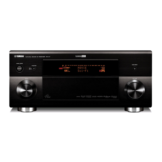
Page 4: Front Panels
RX-Z7/DSP-Z7 ■ FRONT PANELS RX-Z7 (U, C models) U model C model RX-Z7 (A model) - Page 5 RX-Z7/DSP-Z7 DSP-Z7 (R, T, K, B, G, E, L models) DSP-Z7 (J model)
-
Page 6: Rear Panels
RX-Z7/DSP-Z7 ■ REAR PANELS RX-Z7 (U model) RX-Z7 (C model) - Page 7 RX-Z7/DSP-Z7 RX-Z7 (A model) DSP-Z7 (R model)
- Page 8 RX-Z7/DSP-Z7 DSP-Z7 (T model) DSP-Z7 (K model)
- Page 9 RX-Z7/DSP-Z7 DSP-Z7 (B model) DSP-Z7 (G, E models)
- Page 10 RX-Z7/DSP-Z7 DSP-Z7 (L model) DSP-Z7 (J model)
-
Page 11: Remote Control Panels
RX-Z7/DSP-Z7 ■ REMOTE CONTROL PANELS RAV389 RAV391 RAV390 U, C models R, T, K, A, B, G, E, L models J model RAV36... -
Page 12: Specifications
RX-Z7/DSP-Z7 ■ SPECIFICATIONS / ■ Audio Section / Minimum RMS Output Power (Power Amp. Section) / Frequency Response / (10 Hz to 100 kHz) (20 Hz to 20 kHz) CD, etc. to FRONT L/R (Pure direct) ........+0/-3 dB FRONT L/R... - Page 13 RX-Z7/DSP-Z7 ■ FM Section [U, C, A models] Tuning Range Finish / U, C models ............87.5 to 107.9 MHz [RX-Z7] A model ............87.50 to 108.00 MHz Black color ............. U, C, A models [DSP-Z7] 50dB Quieting Sensitivity (IHF) Gold color ............
- Page 14 • DIMENSIONS / This product is manufactured under license from Neural Audio Corporation and THX Ltd. YAMAHA CORPORATION hereby grants the user a non- exclusive, non-transferable, limited right of use to this product under U.S.A. and foreign patent, patent pending and other technology or trademarks owned by Neural Audio Corporation and THX Ltd.
- Page 15 RX-Z7/DSP-Z7 • SELECT MENU Sound Category Field Hall in Munich Hall in Vienna Hall in CLASSICAL Amsterdam Church in Freiburg Chamber Village Vanguard Warehouse Loft LIVE/CLUB Cellar Club The Roxy Theatre The Bottom Line Sports Action Game ENTER- Roleplaying TAINMENT...
- Page 16 RX-Z7/DSP-Z7 • SET MENU TABLE / MANUAL SETUP (GUI) MAIN MENU SUB MENU PARAMETER VALUE [INITIAL VALUE] 1 SPEAKER MENU CONFIG. FRONT SP [SMALL] / LARGE CENTER SP NONE / [SMALL] / LARGE SUR. L/R SP SUR. B L/R SP...
- Page 17 RX-Z7/DSP-Z7 MAIN MENU SUB MENU PARAMETER VALUE [INITIAL VALUE] FRONT PR. L FRONT PR. R REAR PR. L (J model) [MUTE OFF] / MUTE ON REAR PR. R (J model) SWFR 4 VIDEO MENU A) ANALOG –> ANALOG [CONVERSION] / THROUGH B) ANALOG –>...
-
Page 18: Internal View
RX-Z7/DSP-Z7 ■ INTERNAL VIEW Rear view D-VIDEO (1) P.C.B. A-VIDEO P.C.B. FUNCTION (1) P.C.B. FUNCTION (2) P.C.B. HD Radio Tuner (U model) AM/FM Tuner (C, A models) DCCNVT (2) P.C.B. POWER (4) P.C.B. POWER (2) P.C.B. (R, L models) MAIN (3) P.C.B. -
Page 19: Disassembly Procedures
RX-Z7/DSP-Z7 ■ DISASSEMBLY PROCEDURES / (Remove parts in the order as numbered.) Disconnect the power cable from the AC outlet. 1. Removal of Top Cover a. Remove 2 screws ( ), 8 screws ( ) and 5 screws ( (Fig. 1) b. - Page 20 RX-Z7/DSP-Z7 When checking the P.C.B.s: • Spread the rubber sheet and the cloth. Then place the sub chassis unit on the cloth and check it. (Fig. 3) • Reconnect all cables (connectors) that have been disconnected. Be sure to use the extension cable for servicing for the following section.
- Page 21 RX-Z7/DSP-Z7 4. Removal of D-VIDEO (1) P.C.B. a. Remove screw ( ). (Fig. 4) b. Remove the frame side L. (Fig. 4) c. Remove 4 screws ( ). (Fig. 4) d. Remove 6 screws ( ). (Fig. 6) e. Remove CB204, CB953 and CB957. (Fig. 5) f.
- Page 22 RX-Z7/DSP-Z7 U, C, R, T, K, A, B, G, E, L models (R, L models) (U, C, R, T, A, B, G, E, L models) J model Fig. 6...
- Page 23 RX-Z7/DSP-Z7 When checking the P.C.B.s: • Put the rubber sheet and the cloth over this unit. Then place the D-VIDEO and A-VIDEO P.C.B.s up- side down on the cloth and check them. (Fig. 7) • Reconnect all cables (connectors) that have been disconnected.
- Page 24 RX-Z7/DSP-Z7 6. Removal of Rear Unit a. Remove 10 (U, C, T, K, A, B, G, E models) / 12 (R, L models) screws ( ) and 4 (U, C, R, T, A, B, G, E, L models) / 2 (K model) screws ( ).
- Page 25 RX-Z7/DSP-Z7 When checking the P.C.B.s: • Put the rubber sheet and the cloth over this unit. Then place the rear unit upside down on the cloth and check it. (Fig. 9) • Reconnect all cables (connectors) that have been disconnected. Be sure to use the extension cable for servicing for the following section.
- Page 26 RX-Z7/DSP-Z7 7. Removal of Amp Unit a. Remove 2 screws ( ), 5 screws ( ) and 2 screws ( (Fig. 10) b. Remove CB11, CB15 and CB253. (Fig. 10) c. Remove the amp unit. (Fig. 10) CB253 CB11 CB15 POWER (1) P.C.B.
- Page 27 RX-Z7/DSP-Z7 When checking the P.C.B.s: • Put the rubber sheet and the cloth over this unit. Then put the amp unit upright on the cloth and check it. (Fig. 11) • Put the amp unit together with the heat sink upright and check.
-
Page 28: Updating Firmware
RX-Z7/DSP-Z7 ■ UPDATING FIRMWARE / Note) The user memories (sound field parameters, system memory, tuner presetting, etc.) are kept stored even when you write the firmware. When replacing the following parts, be sure to write the latest firmware. P.C.B. Ass’y DSP, FUNCTION or D-VIDEO P.C.B.s IC540 (DSP flash ROM) of DSP P.C.B. - Page 29 RX-Z7/DSP-Z7 Note: With this unit, it is possible to check the firmware version and checksum by using the ADVANCED SETUP menu. 1. While pressing the “STRAIGHT” key of this unit, press the “MASTER ON/OFF” switch of this unit to turn on the power.
- Page 30 RX-Z7/DSP-Z7 ● Operation procedures 1. Download the latest firmware from the specified download source to PC. 2. Copy the latest firmware into the root folder of the USB flash memory. Note) When the firmware is copied into the sub- folder, it is impossible to update firmware.
- Page 31 1 to 5 all over again. Error display / Contents / File error The firmware is not applicable to RX-Z7/DSP-Z7. INVALID FILE RX-Z7 DSP-Z7 USB flash memory error The USB flash memory is damaged.
-
Page 32: Self-Diagnostic Function
RX-Z7/DSP-Z7 ■ SELF-DIAGNOSTIC FUNCTION / There are 30 main menu items, each of which has sub- menu items. Listed in the table below are menu items and sub-menu items. MAIN MENU SUB-MENU A: Audio (Audio system / DSP THROUGH 1. MARGIN 2. - Page 33 RX-Z7/DSP-Z7 MAIN MENU SUB-MENU 14. ZONE2, 3, 4 INPUT : NET/USB 15. ZONE2, 3, 4 INPUT : SIRIUS (U, C models) R: Radio (Tuner and Satellite broadcasting system / XM TEST 1. 1k -1dB/44.1k 2. 1k -61dB/44.1k (U, C models) 3.
- Page 34 RX-Z7/DSP-Z7 MAIN MENU SUB-MENU V: Video (Video system / A-VIDEO P.C.B. CHECK 1. ANALOG BYPASS 2. DIGITAL BYPASS 3. REC ZONE 4. MUTE CHECK 1 5. MUTE CHECK 2 6. OSD character pattern 1 (0-127) 7. OSD character pattern 2 (128-255) 8.
- Page 35 “MASTER ON/OFF” switch to turn on the power and keep pressing those 2 keys. When the “DIAGNOSTIC RX-Z7” (U, C, A models) / “DIAGNOSTIC DSP-Z7 (R, T, K, B, G, E, L models) is displayed, release those 2 keys.
- Page 36 RX-Z7/DSP-Z7 ● Canceling Self-Diagnostic Function ➀ Before canceling self-diagnostic function, execute setting for PRESET of main menu No. S3 (Memory ini- tialization inhibited or Memory initialized). In order to keep the user memory stored, be sure to select PRESET INHIBIT (Memory initialization inhibited).
- Page 37 RX-Z7/DSP-Z7 When there is a history of protection function due to a short between speaker terminals When there is a history of protection function due to a short between speaker terminals Firmware version Cause: The line between speaker terminals is shorted.
- Page 38 RX-Z7/DSP-Z7 When there is a history of protection function due to abnormal DC output A/D conversion value of voltage Firmware version Cause: DC output of the power amplifier is abnormal. (Normal value: 5 to 34) Supplementary information: The abnormal voltage is displayed in based on 5V as 255.
- Page 39 RX-Z7/DSP-Z7 ● Display during menu operation During the self-diagnostic function mode, the monitor screen shows the wall paper and the selected function among following functions as a short message. • Input selection, multi channel input • Muting • Master volume The FL display of this unit shows the selected function.
- Page 40 RX-Z7/DSP-Z7 ● Functions in Self-Diagnostic Function mode In addition to the self-diagnostic function menu items, functions listed below are available. • Input selection, Multi channel input • Center/Rear/Rear center/Sub-woofer level adjustment • Muting • Power on/off • Master volume Functions related to the tuner and the set menu are not available.
- Page 41 RX-Z7/DSP-Z7 ● Details of Self-Diagnostic Function menu With full-bit output specified in some modes, it is possible to execute 0dBFS output without head margin in each channel. – A: Audio (Audio system) – A1. DSP THROUGH This function is for DSP2 only. Main DSP of DSP2 is se- lected for FRONT output.
- Page 42 RX-Z7/DSP-Z7 DSP THROUGH (ANALOG) 64Mbit SDRAM DIR L/R Analog AD L/R PCM1804 SL/SR SBL/SBR or PL/PR Digital SWL/SWR POST PL/PR DECODE PROCESSING LC89057 DSP1 DA70Y DSP2 DA70Y (Shaded items not used in this mode) A2. BYPASS ANALOG BYPASS INPUT: DVD ANALOG...
- Page 43 RX-Z7/DSP-Z7 ANALOG BYPASS (ANALOG) 64Mbit SDRAM DIR L/R Analog AD L/R PCM1804 SL/SR SBL/SBR or PL/PR Digital SWL/SWR POST PL/PR DECODE PROCESSING LC89057 DSP1 DA70Y DSP2 DA70Y (Shaded items not used in this mode) DSP BYPASS (DIGITAL) 64Mbit SDRAM DIR L/R...
- Page 44 RX-Z7/DSP-Z7 A3. HDMI AUDIO The audio signals input to HDMI IN are selected by the sub-menu and output. When you select DSD Direct, be sure to connect an HDMI unit with DSD output function. AUTO DSD Direct DSD (Direct Stream Digital) is output by the direct mode.
- Page 45 RX-Z7/DSP-Z7 The analog switch settings for each sub-menu are as shown in the table below. SURROUND PRESENCE ZONE2 SUB MENU FRONT CENTER SURROUND BACK (SP1) (SP2) WOOFER 1. LFE/B: FRONT LARGE LARGE LARGE LARGE – – FRONT 2. PRESENCE MIX –...
- Page 46 RX-Z7/DSP-Z7 A5. MULTI CH INPUT It is possible to select the 6ch/8ch input and 6-ohm/8- ohm by using the sub-menu. 6CH INPUT_6-ohm INPUT: MULTI CH INPUT SPEAKER OUT: 1kHz, SUBWOOFER OUTPUT: 50Hz SPEAKER OUT SUBWOOFER Input level Volume SURROUND PRESENCE...
- Page 47 RX-Z7/DSP-Z7 8CH INPUT_6-ohm SP INPUT: MULTI CH INPUT SPEAKER OUT: 1kHz, SUBWOOFER OUTPUT: 50Hz SPEAKER OUT SUBWOOFER Input level Volume FRONT SURROUND PRESENCE ZONE2 CENTER SURROUND OUTPUT (DVD) BACK (SP1) (SP2) Both ch, -20 dBm +6.5 dB +13.0 dBm -∞...
- Page 48 RX-Z7/DSP-Z7 A7. MANUAL TEST The noise generator with a built-in DSP outputs the test noise through the channels specified by the sub- menu. The noise frequency for LFE is 30 to 80 Hz. Other than that, the noise frequency is 500 to 2 kHz.
- Page 49 RX-Z7/DSP-Z7 – G: Graphic (Display system) – G1. FL CHECK This menu is used to to check the FL display section. Using the sub-menu operation, the display status of the FL display section vary as shown below. The audio signal is processed using EFFECT OFF. (The L/R signal is output using ANALOG MAIN BYPASS.)
- Page 50 RX-Z7/DSP-Z7 – Z: Zone (Zone function confirmation item) – Z1. ZONE TEST (U, C, R, T, K, A, B, G, E, L models) The INPUT source selected from SUB-MENU is out- put to ZONE 2, 3, 4. ZONE2, 3, 4 INPUT : BD/HD DVD...
- Page 51 RX-Z7/DSP-Z7 ZONE2, 3, 4 INPUT : TUNER ZONE2, 3, 4 INPUT : PHONO ZONE2, 3, 4 INPUT : XM (U, C models) ZONE2, 3, 4 INPUT : NET/USB ZONE2, 3, 4 INPUT : SIRIUS (U, C models) – R: Radio (Tuner and Satellite broadcasting system) –...
- Page 52 RX-Z7/DSP-Z7 XM Tone/44.1k The XM tone (44.1kHz) is output. ISO Tone/44.1k The ISO tone (44.1kHz) is output. 1k -1dB/32k The test tone (1kHz, -1dB/32kHz) is output. 1k -61dB/32k The test tone (1kHz, -61dB/32kHz) is output. Mute /32k Nothing is output.
- Page 53 RX-Z7/DSP-Z7 R2. SIRIUS TEST (U, C models) SIRIUS: Connection of the SIRIUS antenna module is checked. OK : Normal NG : Abnormal – : No connected The connection information of the SIRIUS antenna module is displayed. The result of antenna diagnostic mode (status)
- Page 54 RX-Z7/DSP-Z7 R3. HD RADIO TEST (U model) CPU version The firmware version is displayed. DIR version The DIR version is displayed. DOCK version The DOCK version is displayed.
- Page 55 RX-Z7/DSP-Z7 – U: Universal (Special terminal system (USB, Dock)) – U1. DOCK This menu is used to check the DOCK connector with- out the iPod itself. With the power to this unit turned off, short between pins No. 14 (TX) and No. 18 (RX), between pins No.
- Page 56 RX-Z7/DSP-Z7 U2. USB CHECK VNP2 TEST 1k 1kHz test tone is output. VNP2 TEST 20Hz 20Hz test tone is output. VNP2 TEST 20k 20kHz test tone is output. VNP2 TEST2 1kHz test tone is output. Signal path of test tone output / VNP2 (IC105 D-VIDEO P.C.B.)
- Page 57 RX-Z7/DSP-Z7 The music file recorded in the USB flash memory is reproduced. Copy 2 or more music files from PC into the root folder of the USB flash memory. b. Insert the USB flash memory to the USB terminal of this unit.
- Page 58 RX-Z7/DSP-Z7 – N: Network (Network function system) – N1. NET CHECK When the network condition varies while SUB- MENU is displayed (e.g., the network is deactivated once), the correct result will not be displayed. In that case, once turn off the power to this unit, then start up the self-diagnostic function again and select this menu.
- Page 59 RX-Z7/DSP-Z7 • Operation procedures a. Press the “MENU” key. The digit that can be changed is indicated with [ Digit that can be changed Press b. Turn the “PROGRAM” knob to change the alpha- numerical letter in the first digit.
- Page 60 RX-Z7/DSP-Z7 d. Repeat steps b. and c. to change all settings to the MAC address number of the old D-VIDEO P.C.B.. Last digit e. Press the “MENU” key. The procedure is completed when “OK” is displayed. Press LINK CHECK LAN cable connection is checked.
- Page 61 RX-Z7/DSP-Z7 Ext loopback test This menu is used to check the NETWORK connector. With the power to this unit turned off, short between pins No. 1 (Tx+) and No. 3 (Rx+) and between pins No. 2 (Tx-) and No. 6 (Rx-) of the NETWORK connector.
- Page 62 RX-Z7/DSP-Z7 – C: Communication (Communication and BUS line check item, etc..) – C1. FUNCTION P.C.B. CHECK This menu is used to check transmission of the data and the flow port of the hardware. With the power to this unit turned off, short between pins No.
- Page 63 RX-Z7/DSP-Z7 C2. DSP P.C.B. CHECK Communication and bus line connection between devices on the DSP P.C.B. are checked. TI1 (DSP1) BUS The TI1 (DSP1, IC534) bus line connection is checked. : No error detected : An error is detected TI2 (DSP2) BUS The TI2 (DSP2, IC567) bus line connection is checked.
- Page 64 RX-Z7/DSP-Z7 C3. D-VIDEO P.C.B. CHECK Communication and bus line connection between devices on the D-VIDEO P.C.B. are checked. ALL Check The synthetic judgment result is displayed. : No error detected : An error is detected No Check : Detection is not executed SDRAM BUS Check Read/Write of SDRAM (IC104, IC125) is checked.
- Page 65 The product ID of this unit written in HDMI module is displayed. 3132: RX-Z7 (U, C, A models) 3131: DSP-Z7 (R, T, K, B, G, E, L, J models) HDMI Vendor Name The vendor name (YAMAHA) of this unit written in the HDMI module is displayed.
- Page 66 RX-Z7/DSP-Z7 C5. EPROM CHECK SPI-EPROM CHECK – V: Video (Video system) – V1. A-VIDEO P.C.B. CHECK The video signal is converted and output as shown below. ANALOG BYPASS ANALOG BYPASS DVIDEO P.C.B. Video Decoder Video Encoder ADV7800 ADV7342 IC701 IC702...
- Page 67 RX-Z7/DSP-Z7 DIGITAL BYPASS DIGITAL BYPASS DVIDEO P.C.B. Video Decoder Video Encoder ADV7800 ADV7342 IC701 IC702 MONITOR OUT INPUT Selector IC201 Bypass INPUT Selector MONITOR OUT Selector IC221 IC213,215 SOURCE/REC Selector REC OUT REC/ZONE IC217 Selector IC214,216 Bypass INPUT Selector CVBS...
- Page 68 RX-Z7/DSP-Z7 MUTE CHECK 1 MUTE signal “VMT” (92 pin) is output from the sub- microprocessor (FUNCTION P.C.B. IC402). MUTE CHECK 2 • MUTE signals “MON_N_VMT” (AE4) and “Z2_N_VMT” (AD4) are output from the NPGA (D-VIDEO P.C.B. IC114). • MUTE signals “/MTVR1 (18 pin)” and “/MTVR2 (17 pin)”...
- Page 69 RX-Z7/DSP-Z7 TEST PATTERN Test pattern DVIDEO P.C.B. Video Decoder Video Encoder ADV7800 ADV7342 IC701 IC702 MONITOR OUT INPUT Selector IC201 Bypass INPUT Selector MONITOR OUT Selector IC221 IC213,215 SOURCE/REC Selector REC OUT REC/ZONE IC217 Selector IC214,216 Bypass INPUT Selector CVBS...
- Page 70 RX-Z7/DSP-Z7 V2. D-VIDEO P.C.B. ROUTE CHECK The video signal route as shown below is checked. HDMI loop-back test TEST1 Loop-back check 1 Front-HDMI-Board HDMI Cable for Loopback CB703 HDMI EQ HDMI CXB1442 Front IC752 IC753 256Mbit 256Mbit DDR2 DDR2 CB704...
- Page 71 RX-Z7/DSP-Z7 TEST3 Test pattern 480p to 1080p (I/P Scalar check) Front-HDMI-Board CB703 HDMI EQ HDMI CXB1442 Front IC752 IC753 256Mbit 256Mbit DDR2 DDR2 CB704 CB705 CB706 CB707 CB708 CB709 HDMI HDMI HDMI HDMI HDMI HDMI IC751 OUT1 OUT2 I/P Scalar...
- Page 72 RX-Z7/DSP-Z7 HDMI to HDMI_out1 Front-HDMI-Board CB703 HDMI EQ HDMI CXB1442 Front IC752 IC753 256Mbit 256Mbit DDR2 DDR2 CB704 CB705 CB706 CB707 CB708 CB709 HDMI HDMI HDMI HDMI HDMI HDMI IC751 OUT1 OUT2 I/P Scalar ABT2010 IC726 IC728 IC729 IC732 HDMI SW...
- Page 73 RX-Z7/DSP-Z7 CVBS to DA and HDMI_out1 with DDR Front-HDMI-Board CB703 HDMI EQ HDMI CXB1442 Front IC752 IC753 256Mbit 256Mbit DDR2 DDR2 CB704 CB705 CB706 CB707 CB708 CB709 HDMI HDMI HDMI HDMI HDMI HDMI IC751 OUT1 OUT2 I/P Scalar ABT2010 IC726...
- Page 74 RX-Z7/DSP-Z7 Component_480p to DA and HDMI_out1 Front-HDMI-Board CB703 HDMI EQ HDMI CXB1442 Front IC752 IC753 256Mbit 256Mbit DDR2 DDR2 CB704 CB705 CB706 CB707 CB708 CB709 HDMI HDMI HDMI HDMI HDMI HDMI IC751 OUT1 OUT2 I/P Scalar ABT2010 IC726 IC728 IC729...
- Page 75 RX-Z7/DSP-Z7 YGV to DA and HDMI_out1 Front-HDMI-Board CB703 HDMI EQ HDMI CXB1442 Front IC752 IC753 256Mbit 256Mbit DDR2 DDR2 CB704 CB705 CB706 CB707 CB708 CB709 HDMI HDMI HDMI HDMI HDMI HDMI IC751 OUT1 OUT2 I/P Scalar ABT2010 IC726 IC728 IC729...
- Page 76 RX-Z7/DSP-Z7 – P: Power Supply (Power supply system) – P1. SYSTEM MONITOR This menu is used to display the A/D conversion value of the main microprocessor which detects panel keys of this unit and protection functions by using the sub-menu. Signal processing is maintained in the status before execution.
- Page 77 RX-Z7/DSP-Z7 TM1/TM2 (Temperature detection) Temperature detected value (Normal value: 10 to 83) TM1: Detects the temperature of the heat sink at the left side (power transformer side) TM2: Detects the temperature of the heat sink at the right side (volume side)
- Page 78 RX-Z7/DSP-Z7 AMPRELAY (Amp. Power relay control) Use the “PURE DIRECT” key to change the output of the relay for power supply of the amplifier (RY250, RY251 MAIN (2) P.C.B.). VAR.: Variable LOW: RY250 ON, RY251 ON MID: RY250 OFF, RY251 ON...
- Page 79 (standard value ±4), normal operation will not be available. In this case, check the constant of voltage dividing resistor, solder condition, etc. Refer to table. (Reference voltage: 5V=255) RX-Z7 (U, C, A models) Display INFO STRAIGHT / EFFECT 26±4...
- Page 80 RX-Z7/DSP-Z7 P2. PROTECTION HIST. The history of protection function is displayed. After selecting the sub-menu, press the “STRAIGHT” key, and the history will be erased. Last Example History1 Example Protection name H: When the upper limit of the protection function is exceeded.
- Page 81 RX-Z7/DSP-Z7 – S: System (System setting confirmation item) – S1. FIRM UPDATE Not applied to these models. CPU UPDATE : ALL CPU UPDATE : VNP2 CPU UPDATE : M32C CPU UPDATE : TI S2. TOOL UPDATE Not applied to these models.
- Page 82 RX-Z7/DSP-Z7 S3. FACTORY PRESET This menu is used to reserve and inhibit initializa- tion of the back-up RAM. The signals are processed using EFFECT OFF. (The L/R signal is output using ANALOG MAIN BYPASS.) PRESET INHIBIT (Initialization inhibited) / RAM initialization is not executed. Select this sub-menu to protect the values set by the user.
- Page 83 RX-Z7/DSP-Z7 S4. ROM VER/SUM The version and checksum are displayed. The signal is processed using EFFECT OFF. The checksum is obtained by adding the data at every 8 bits for each program area and expressing the result as a 4-figure hexadecimal data.
- Page 84 RX-Z7/DSP-Z7 S5. SET INFO. The information on the model are displayed. MODEL: RX-Z7, DSP-Z7 The model name is displayed. DEST.: U, C, R, T, K, A, BGE, L, J U, C, R, T, K, A, B, GE, L or J is displayed.
-
Page 85: Amp Adjustment
RX-Z7/DSP-Z7 ■ AMP ADJUSTMENT / Confirmation of Idling Current of Amp Unit ● Right after power is turned on, confirm that the volt- age across the terminals of R467 (SURROUND BACK F R O N T R c h Rch), R468 (SURROUND Rch), R469 (FRONT Rch),... -
Page 86: Display Data
RX-Z7/DSP-Z7 ■ DISPLAY DATA • V9001: HNA-16ML15T (FL P.C.B.) PATTERN AREA • PIN CONNECTION Pin No. 130 129 128 127 126 125 124 123 122 121 120 119 118 117 116 115 114 113 112 111 110 109 108 107 106 105 104 103 102 101 100 99... - Page 87 RX-Z7/DSP-Z7 • ANODE CONNECTION 1GA-14GA 15GA 16GA 1GB-14GB 15GB 1-1A 1-1B 2-1B 2-1A 3-1A 3-1B 4-1A 4-1B 5-1B 5-1A 1-2A 1-2B 2-2A 2-2B 3-2A 3-2B 4-2B 4-2A P10A 5-2A P10B 5-2B P11A 1-3A P11B 1-3B P12A 2-3A P12B 2-3B P13B...
-
Page 88: Ic Data
RX-Z7/DSP-Z7 ■ IC DATA IC534, 567: D70YE101BRFP266 (DSP P.C.B.) Decoder/Post processor * No replacement part available. / SPI0_SIMO EM_CKE SPI0_SOMI/I2C0_SDA EM_CLK AXR0[0] EM_WE_DQM[1] AXR0[1] EM_D[8] AXR0[2] AXR0[3] EM_D[9] EM_D[10] AXR0[4] AXR0[5]/SPI1_SCS EM_D[11] AXR0[6]/SPI1_ENA AXR0[7]/SPI1_CLK EM_D[12] EM_D[13] EM_D[14] AXR0[8]/AXR1[5]/SPI1_SOMI EM_D[15] AXR0[9]/AXR1[4]/SPI1_SIMO... - Page 89 RX-Z7/DSP-Z7 Function Name TYPE PULL GPIO Detail of Function (P.C.B.) AHCLKX0/AHCLKX2 – McASP0 and McASP2 transmit master clock AMUTE0 – McASP0 mute output AMUTE1 – McASP1 mute output AHCLKX1 – McASP1 transmit master clock ACLKX1 – McASP1 transmit bit clock...
- Page 90 RX-Z7/DSP-Z7 Function Name TYPE PULL GPIO Detail of Function (P.C.B.) EM_D[10] – EMIF data bus [lower 16-Bits] EM_D[9] – EMIF data bus [lower 16-Bits] CVDD EM_D[8] – EMIF data bus [lower 16-bits] EM_WE_DQM[1] – Write enable or byte enable for EM_D [15:8]...
- Page 91 RX-Z7/DSP-Z7 Function Name TYPE PULL GPIO Detail of Function (P.C.B.) 123 CVDD 124 VSS 125 DVDD McASP0 serial data 8 or McASP1 serial data 5 or SPI1 data pin slave 126 /SPI1_SOMI – out master in McASP0 serial data 9 or McASP1 serial data 4 or SPI1 data pin slave in 127 /SPI1_SIMO –...
- Page 92 RX-Z7/DSP-Z7 IC402: M3087BFKBGP (FUNCTION P.C.B.) Main microprocessor Port P0 Port P1 Port P2 Port P3 Port P4 Port P5 Port P6 < > < > CC1 (3) Peripheral Functions Clock Generation Circuit A/D Converter: 1 circuit Timer (16 bits) Standard: 10 inputs...
- Page 93 RX-Z7/DSP-Z7 Function Port Name Name Detail of Function (P.C.B.) Asynchronous data output for SIRIUS (U, C models) TXD4 SIRTXD Hardware connection is NC / Perform Low Fix treatment also when power on (R, T, K, A, B, G, E, L, J models)
- Page 94 RX-Z7/DSP-Z7 Function Port Name Name Detail of Function (P.C.B.) HD-Radio connection is NC / Perform Low Fix treatment also when power on – (U model) 30 CLK5 TUCK PLL clock output for tuner (C, A models) Hardware connection is NC / Perform Low Fix treatment also when power on –...
- Page 95 RX-Z7/DSP-Z7 Function Port Name Name Detail of Function (P.C.B.) – Pull-down to GND when HD-Radio is connected (U model) 55 P54/HLDA TUNER STEREO detection input (C, R, T, K, A, B, G, E, L, J models) Pull-up to +5SPC T-CONT/EVOL IC serial transmission clock for ZONE...
- Page 96 RX-Z7/DSP-Z7 Function Port Name Name Detail of Function (P.C.B.) 89 P121 RTSR 90 TXD6 TXDR 91 Vcc MCU MCU MCU Video output MUTE / This port is logically inverted at ON*Tr when Power ON/ 92 P30/A8 OFF and Pure Direct ON/OFF...
- Page 97 RX-Z7/DSP-Z7 Function Port Name Name Detail of Function (P.C.B.) Data output for FL DRIVER IC / PT6302 118 P110 SDTN Data output for expanded IC / LC709004A Max. 2MHz when using VDD=4.5 to 6V 119 P03/AN03/D3 Volume rotary B 120 P02/AN02/D2...
- Page 98 Headphone detection / 100k pull-up to +5SPC 14 P11 (U, C, R, T, K, A, B, G, E, F, L models) 13 P12 12 P13 11 P14 10 P15 RX-Z7 (U, C, A models) Key input(A-D) pull-up resistance 10 k-ohms +1.2k +1.2k +1.8k +2.7k +3.3k +4.7k...
- Page 99 RX-Z7/DSP-Z7 IC105: YTD-446CZ (D-VIDEO P.C.B.) VNP2 (Video and network processor) * No replacement part available. / GPIO Memory I/F Interrupt ARM926EJ-S Controller Memory ARM9EJ-S Controller0 UART0 Dual Timer0 I-cache D-cache UART1 Dual Timer1 16KB 16KB Memory UART2 Watchdog Controller1 Timer...
- Page 100 RX-Z7/DSP-Z7 Pin No. Port Name Function Name (P.C.B.) Detail of Function nRESET VNP2_N_RST System reset terminal XI_S System clock crystal oscillation terminal XO_S System clock crystal oscillation terminal AE24 XI_A Audio clock crystal oscillation terminal AD24 XO_A Audio clock crystal oscillation terminal...
- Page 101 BGPIO[2] NUDAC_MUT H: Mute on / L: MUTE off BGPIO[22] IPAP_DET iPod accessory power detection Model discrimination BGPIO[23] Z7_DET H: RX-Z7/DSP-Z7 / L: RX-V3900/DSP-3900 (Applicable only when testing P.C.B.) SDO_ABCK VNP2_BCK Bit clock output for audio SDO_BBCK/BGPIO[11] – SDO_AWCK VNP2_LRCK...
- Page 102 RX-Z7/DSP-Z7 Pin No. Port Name Function Name (P.C.B.) Detail of Function AC17 USB_OC USB excess current detection AE12 MAC_REF_CLK RMII clock output AE13 MAC0_RXD0 RMII reception data AD13 MAC0_RXD1 RMII reception data AC13 MAC0_RXER RMII reception error AE14 MAC0_TXD0 RMII transmission data...
- Page 103 RX-Z7/DSP-Z7 IC114: MB87L8760 (D-VIDEO P.C.B.) NPGA * No replacement part available. / Pin No. Port Name Function Name (P.C.B.) Detail of Function PIO[0] VDEC_N_INT Interrupt from ADV7800 PIO[1] HTX1_N_INT Interrupt from SII9134 #1 PIO[2] HTX2_N_INT Interrupt from SII9134 #2 PIO[3]...
- Page 104 RX-Z7/DSP-Z7 Pin No. Port Name Function Name (P.C.B.) Detail of Function Video monitor signal mute PIO[27] MON_N_VMT_3 L: Mute on / H: Mute off TXD1 – RXD1 – PI5_XCTS1 – PO5_XRTS1 – PIO[9] HTX2_N_RST Resetting for SII9134 #2 PIO[10] HRX_N_RST...
- Page 105 RX-Z7/DSP-Z7 Pin No. Port Name Function Name (P.C.B.) Detail of Function A[0] SA[0] HOST I/F address bus XTCK For testing PIO[28] Z2_N_VMT_3 Zone2 video mute PIO[15] IOEX_N_RST Reset signal to IO expanded device PIO[29] SV_DET S-Video detection signal PIO[30] XIRQ...
-
Page 106: Pin Connection Diagrams
RX-Z7/DSP-Z7 ■ PIN CONNECTION DIAGRAMS • ICs ADV7800BSTZ-80 ADM222ARZ ADV7342BSTZ SiI9134CTU AK4384ET BA15218F BD3841FS BD6517F-E2 CS230003-CZZR CD4051BNSR TC7MBL3257AFK BD3508EKN-E2 BD9011EKN-E2 EP2C8F256C8N D70YE101BRFP266 DSD1791DBR F2621E-01-TR K4S281632K-UC75000 CXB1442AR-T4 M3087BFKBGP YAC523-EVR2 M12L64164A-5TG MB87L8760 KIA7812API KIA7912PI LA7106M-TLM-E LA73050-TLM-E LC72725KM-UY-TLM-E LA73053-TLM-E MM74HC4051SJX MM74HC4053SJX PCM1781DBQR LC89057W-VF4AD-E... - Page 107 RX-Z7/DSP-Z7 IP101ALF K4S641632K-UC75000 NJM2388F05 NJM2388F09 NJM2388F33 1. V 1. V 2. V 2. V 3. GND 3. GND 4. ON/OFF CONTROL 4. ON/OFF CONTROL MN103SFD7G M12L64322A-7TG 0.1UM M13S128168A-6TG NE5532DR NJM2068MD-TE2 NJM2566AV NJM2867F3-05 NJM2885DL1-33 NJM5532M-D TC7SET32FU 2:GND LP2995MX NJU7311AM NJW1194V NJW1321FP1...
- Page 108 RX-Z7/DSP-Z7 R1172S121D-E2-F SiI9135ACTU SiI9185ACTU S29AL016D70TFI020 R1172S181B-E2-F R1172S251B-E2-F R1172S331B-E2-F S29GL128P90TFCR20 SN74AHCT00PWR SN74AHCT08PWR SN74CB3Q3257PWR SN74LV157APWR SN74LVC74APWR SN74LS151NSR TC74VHC153FT TC74VHC125FT SN74LV245APWR SN74LVC245APWR SN74LVU04APWR SN74AHCT1G32DCKR TC74VHCT245AFT TA1318AF TC4013BP TC74HC4052AF TK15420M TC7WH08FK TC7WH14FK TC7WZ04FK V59C1256164QAF25 YGV619 YTD446-CZ...
- Page 109 RX-Z7/DSP-Z7 • Diodes 1N4002S 1SS355 MA8100-M 10.0V D2SBA20 1SS380 MA8130-M MTZJ5.1C MA8030-L MA8160-H 16.7V MA8240-M MA-8039-H MA8047 RB501V-40 Anode MA8047-L RB160M-30 Anode MA8051-M RB160M-60 TR MA8056-M RB500V-40 – UDZS5.6BTE-17 MA8062-M Cathode MA8068-M Cathode MA8075-M D15XBN20 DB105 MA8024-(TX) 2.4V D4SBS6-7101 D20XBS6-7101 Anode –...
- Page 110 RX-Z7/DSP-Z7 • Transistors 2SA949 2SA2168 2SB1257 A2151/C6011 2SK3850 2SA1036KT146 2SC1815 2SB1274 2SA1037K 2SC5291 2SC3852 2SC2229 2SA1576A 2SD2014 2SC2878 2SC2412K 2SC3326 2SC3837K 2SC3906K 2SC4081 2SD1938F 2SK208 KRA102S-RTK/P KTA1504S KTA1046-Y-U/P DTA143EKA 5HP01C-TB-E KRA104S-RTK KTA1517S DTC114EKA KRC102S-RTK KTC3875S DTC144EKA KRC104S-RTK KTC3911S COLLECTOR 1: GND...
-
Page 111: Block Diagrams
RX-Z7/DSP-Z7 ■ BLOCK DIAGRAMS AUDIO SECTION BLOCK DIAGRAM IC108 SII9185A MPCM/DSD IC726 IC727 Sil9135 • See page 149-151 → SII9185A SCHEMATIC DIAGRAM IC728 DSD Direct IC729 D-VIDEO Sil9134 OUT1 • See page 161-171 → DSP BYPASS IC732 OUT2 SCHEMATIC DIAGRAM... - Page 112 RX-Z7/DSP-Z7 VIDEO SECTION BLOCK DIAGRAM HDMI Pb/Cb FRONT IN OUT1 OUT2 MONITOR OUT CEC1 CEC2 Pr/Cr (ZONE4 OUT) CVBS and YC INPUT/RECOUT SELECTOR (4051) Relay RY700 INPUT VIA/VRA VIB/VRB VIC/VRC /VMT J model POWERSAVE iPod /MTMON Pb/Cb IC203 V-AUX Pr/Cr...
- Page 113 RX-Z7/DSP-Z7 D-VIDEO SECTION BLOCK DIAGRAM Communication UART 5V tolerant VCPU_TXD VCPU_RXD VCPU_N_CTS VCPU_N_RTS V M_N_INT HDMI_INT iPOD control UART 5V tolerant IPD_TXD IPD_RXD iPOD mount detect IPAP_DET OSD_N_SCK OSD control SPI OSD_MOSI DBG_TXD OSD_N_CS DBG_RXD DBG_LED0,DBG_LED1 IRQ from MAIN CPU...
- Page 114 RX-Z7/DSP-Z7 POWER SUPPLY SECTION BLOCK DIAGRAM PCB-DVIDEO [HDMI Interface Block] PCB-POWER (1) PCB-FUNC (1) D-VIDEO • See page 158 → • See page 152, 153 → HDMI Equalizer POWER (1) FUNCTION (1) +1.8EQ • See page 161-171 → Regulator HDMI Repeater...
- Page 115 RX-Z7/DSP-Z7 CONTROL SECTION BLOCK DIAGRAM • See page 157 → MAIN SCHEMATIC DIAGRAM • See page 154, 155 → FUNCTION (2) • See page 172, 173 → SCHEMATIC DIAGRAM SELECTOR FL1/2 SCHEMATIC DIAGRAM NJU7311AM IC301 ID=0h Audio Power Relay FUNCTION (1)
-
Page 116: Printed Circuit Boards
RX-Z7/DSP-Z7 ■ PRINTED CIRCUIT BOARDS DSP P.C.B. (Side A) DIGITAL INPUT DIGITAL OUTPUT COAXIAL OPTICAL U, C models DOCK BD/HD DVD CBL/SAT MD/CD-R No replacement part available. CB502 CB501 OPERATION (3) (CB805) IC501 No replacement part available. DGND +5D1 FL (5) - Page 117 RX-Z7/DSP-Z7 DSP P.C.B. (Side B) U, C models R5001 • Semiconductor Location Ref No. Location side B D5301 D5302 D5303 D5306 D5308 D5309 D5310 D5311 D5600 D5601 D5602 D5603 D5604 D5605 D5606 D5607 Q5001 Q5002 Q5301 U, C models Circuit No.
- Page 118 RX-Z7/DSP-Z7 Circuit No. C, R, T, K, A, L B, G, E C4520, 4521, 4523, 4528 IC450 J4506, 4507, 4512, 4513 FUNCTION (1) P.C.B. (Side A) J4510, 4511 R, T, K, B, G, E, L, J models VIDEO U, C, R, T, K, A, B, G, E, L models...
- Page 119 RX-Z7/DSP-Z7 FUNCTION (1) P.C.B. (Side B) U, C, R, T, K, A, B, G, E, L models U, C, R, T, K, A, B, G, E, L models U, C models U, C, B, G, E models J model • Semiconductor Location Ref No.
- Page 120 RX-Z7/DSP-Z7 • Semiconductor Location FUNCTION (2) P.C.B. (Side A) Ref No. Location D3000 U, C, R, T, K, A, B, G, E, L models D3002 AUDIO MULTI CH INPUT PRE OUT ZONE OUT D3004 PHONO ZONE 4 CENTER / FRONT (6CH) /...
- Page 121 RX-Z7/DSP-Z7 FUNCTION (2) P.C.B. (Side B) R, T, K, A, B, G, E, L models U, C, R, T, K, A, B, G, E, L models • Semiconductor Location Ref No. Location D3001 D3003 Q3508...
- Page 122 RX-Z7/DSP-Z7 OPERATION (1) P.C.B. OPERATION (4) P.C.B. OPERATION (6) P.C.B. (Side A) (Side A) (Side A) FL (1) (W9003) CB812 RXDF BUSY PURE TXDF W8004B BOOT DIRECT W8006 /RES +5M2 +5SPC KEY1B PDLED +5D1 PROGRAM INPUT FL (2) (CB971) W8003B...
- Page 123 RX-Z7/DSP-Z7 OPERATION (1) P.C.B. OPERATION (4) P.C.B. OPERATION (6) P.C.B. (Side B) (Side B) (Side B) D8020 D8019 • Semiconductor Location OPERATION (2) P.C.B. OPERATION (5) P.C.B. (Side B) (Side B) Ref No. Location D8002 D8003 D8019 D8020 D8023 Q8001...
- Page 124 RX-Z7/DSP-Z7 OPERATION (3) P.C.B. (Side A) VIDEO AUX OPTIMIZER PHONES S-VIDEO VIDEO AUDIO OPTICAL SILENT CINEMA OPERATION (4) (CB810) (Front) JK803 VBus -Data CB811 +Data JK801 JK802 CXB1442_CE CB804 D-VIDEO (1) (CB110) CB807 +5D1 A-VIDEO (W2002) +5D1 FUNCTION (2) (W301A)
- Page 125 RX-Z7/DSP-Z7 OPERATION (3) P.C.B. (Side B) U, C, R, T, K, A, B, G, E, L model J model IC801 IC805 • Semiconductor Location Ref No. Location D8004 D8005 D8006 D8007 D8008 D8009 D8010 D8017 D8018 IC801 IC802 IC805 Q8002...
- Page 126 RX-Z7/DSP-Z7 • Semiconductor Location Ref No. Location Ref No. Location Ref No. Location Ref No. Location Ref No. Location Ref No. Location Ref No. Location D279 Q279 Q288 Q296 Q309A Q313A Q366 MAIN (1) P.C.B. (Side A) D280 Q280 Q289...
- Page 127 RX-Z7/DSP-Z7 MAIN (1) P.C.B. (Side B) • Semiconductor Location Ref No. Location Ref No. Location Ref No. Location Ref No. Location Ref No. Location Ref No. Location Ref No. Location Ref No. Location Ref No. Location Ref No. Location Ref No. Location...
- Page 128 RX-Z7/DSP-Z7 MAIN (2) P.C.B. MAIN (3) P.C.B. MAIN (4) P.C.B. (Side A) (Side A) (Side A) MAIN (4) MAIN (1) (W263A) (W274B) MAIN (1) (W255A) BLACK U, C, R, T, K, A, B, G, E, L models BLUE MAIN (1)
- Page 129 RX-Z7/DSP-Z7 MAIN (2) P.C.B. MAIN (3) P.C.B. MAIN (4) P.C.B. (Side B) (Side B) (Side B) U, C, R, T, K, A, B, G, E, L models U, C, R, T, K, A, B, G, E, L models • Semiconductor Location Ref No.
- Page 130 RX-Z7/DSP-Z7 POWER (1) P.C.B. POWER (1) P.C.B. (Side A) (Side B) POWER TRANSFORMER -BAV DVGReturn DVGReturn +BDV +BDV PRV2 +5D1 +5D1 POWER (3) (CB24) FL (1) (W9001) • Semiconductor Location Ref No. Location...
- Page 131 RX-Z7/DSP-Z7 POWER (2) P.C.B. POWER (6) P.C.B. (Side A) (Side A) R, L models POWER TRANSFORMER POWER (4) (CB6) VOLTAGE SELECTOR VOLTAGE SELECTOR 230-240V 1-2/5-6 CB10 220V 2-3/6-7 110V 3-4/7-8 120V 4-5/8-1 • Semiconductor Location POWER TRANSFORMER Ref No. Location...
- Page 132 RX-Z7/DSP-Z7 POWER (3) P.C.B. (Side A) U, C models POWER TRANSFORMER R, T, K, A, B, G, E, L, J models U, C models DCCNVT (1) IC16 IC15 IC17 (CB71) • Semiconductor Location Ref No. Location A-VIDEO (W2001) CB14 CB24...
- Page 133 RX-Z7/DSP-Z7 POWER (4) P.C.B. POWER (4) P.C.B. (Side A) (Side B) • Semiconductor Location Ref No. Location POWER TRANSFORMER POWER (2) (W2A)(W2B) R, T, K, A, B, G, E, L models (for factory) CB25 /RES POINT D 1 / C2, 2 / Q1...
- Page 134 RX-Z7/DSP-Z7 A-VIDEO P.C.B. (Side A) J model VIDEO D5 VIDEO COMPONENT VIDEO MONITOR OUT CBL/SAT BD/HD DVD CBL/SAT BD/HD DVD CBL/SAT BD/HD DVD MONITOR OUT S VIDEO/VIDEO J model D5 VIDEO JK202 JK203 JK201 IC218 IC203 IC219 IC201 AGND ADPb...
- Page 135 RX-Z7/DSP-Z7 A-VIDEO P.C.B. (Side B) J model J model IC212 IC214 IC216 U, C, R, T, K, A, B, G, E, L models • Semiconductor Location Ref No. Location Ref No. Location Circuit No. U, C, R, T, K, A, B, G, E, L...
- Page 136 RX-Z7/DSP-Z7 Ref No. Location Ref No. Location Ref No. Location Ref No. Location Ref No. Location IC722 IC732 IC751 IC800 Q7000 IC726 IC733 IC752 IC801 Q7009 IC727 IC734 IC753 IC802 Q7010 IC728 IC735 IC754 Q1005 Q7011 D-VIDEO (1) P.C.B. (Side A)
- Page 137 RX-Z7/DSP-Z7 POINT G XL700 (Pin 80 of IC701) POINT H XL701 (OUT) POINT J XL102 (IC105) POINT I XL702 (OUT) POINT K XL101 (Pin 89 of IC114) POINT L XL103 (Pin 103 of IC114) D-VIDEO (1) P.C.B. (Side B) (Writing port) (Writing port)
- Page 138 RX-Z7/DSP-Z7 FL (1) P.C.B. (Side A) POWER (1) (CB12) W9001 OPERATION (5) FL (2) (CB970) (CB809) HPMT +5M2 /MIC KEY1 PSWDET PSW2 PSW1 KEY1B KEY0 +5D1 BT232C CEF1 +5M2 +5M2 +5SPC REM1 CEF2 SCKN OPERATION (1) SDTN /ICFL CATEGORY STEREO/...
- Page 139 RX-Z7/DSP-Z7 FL (1) P.C.B. (Side B) 48 49 16 17 • Semiconductor Location Ref No. Location Ref No. Location D9005 Q9001 D9006 Q9002 D9017 Q9003 D9021 Q9004 D9022 Q9005 D9023 Q9006 D9024 Q9007 D9025 Q9008 D9026 Q9009 IC901 Q9010 IC902...
- Page 140 RX-Z7/DSP-Z7 FL (2) P.C.B. (Side A) D-VIDEO (1) D-VIDEO (1) (CB710) (CB102) OPERATION (2) (CB803) (Writing port) +5D1 PDLED CB953 CB964 KEY1B +5SPC CB957 +5M2 /RES BOOT TXDF BUSY RXDF HPMT /MIC KEY1 PSWDET PSW2 PSW1 KEY1B KEY0 BT232C CEF1...
- Page 141 RX-Z7/DSP-Z7 FL (2) P.C.B. (Side B) IC951 IC952 • Semiconductor Location Ref No. Location D9501 IC951 IC952...
- Page 142 RX-Z7/DSP-Z7 FL (3) P.C.B. FL (4) P.C.B. (Side A) (Side A) FUNCTION (1) (CB404) FUNCTION (1) (CB403) INPR INPR CB955 CB952 INPL INPL TPRR TPRR TPRL TPRL NETR NETR NETL NETL Z2R1 Z2R1 Z2L1 Z2L1 CB956 CB951 FUNCTION (1) FUNCTION (2)
- Page 143 RX-Z7/DSP-Z7 FL (5) P.C.B. FL (6) P.C.B. (Side A) (Side A) TRIGGER OUT RS-232C +12V 15mA MAX. /INTDIR /INTDIR /CSY /CSTI1 /INTTI /INTTI SPIRDY SPIRDY CB991 /ICTI /SPIRDY1 JK991 JK992 /CSTI /CSTI0 DTXM DTXM DRXM DRXM /ICXM /ICXM XMPWR XMPWR...
- Page 144 RX-Z7/DSP-Z7 CONNECT (1) P.C.B. CONNECT (1) P.C.B. (Side A) (Side B) U model U model To HD radio tuner W901 (+5D) -3.3HD POWER (3) R926 (W8) CB903 FUNCTION (1) (CB401) • Semiconductor Location Ref No. Location D900 D901 D904 IC901...
- Page 145 RX-Z7/DSP-Z7 CONNECT (2) P.C.B. CONNECT (2) P.C.B. (Side A) (Side B) U, C models U, C models SIRIUS JK950 • Semiconductor Location IC951 Ref No. Location D950 D952 D953 D954 IC950 IC951 Q951 Q952 W953 FUNCTION (1) (CB451)
- Page 146 RX-Z7/DSP-Z7 DCCNVT (1) P.C.B. DCCNVT (1) P.C.B. (Side A) (Side B) DGReturn DGReturn +2.0DSW +2.0DSW D-VIDEO (1) (CB108) IC71 IC72 PRV2 +2.0DSW PRV2 +4.3DSW +4.3DSW • Semiconductor Location +6.5DSW +2.8DSW Ref No. Location +2.8DSW D701 +6.5DSW POWER (3) D702 (CB14)
- Page 147 RX-Z7/DSP-Z7 DCCNVT (2) P.C.B. DCCNVT (2) P.C.B. (Side A) (Side B) D-VIDEO (1) D-VIDEO (1) (CB112) (CB111) CB61 CB63 NETWORK (Rear)
- Page 148 RX-Z7/DSP-AXZ7 MEMO MEMO...
-
Page 149: Schematic Diagrams
RX-Z7/DSP-Z7 SCHEMATIC DIAGRAMS DSP 1/3 Page 152 Page 156 Page 173 Page 173 to FUNCTION (1)_CB411 to OPERATION (3)_CB805 to FL (2)_CB954 to FL (2)_CB974 12.4 IC510 IC509: SN74LV157APWR Quadruple 2-line to 1-line data selectors/multiplexers IC510 -11.9 IC511 C5099 DUTY CORRECTOR... - Page 150 RX-Z7/DSP-Z7 DSP 2/3 Page 173 Page 173 Page 158 Page 158 to FL (5)_CB973 to FL (5)_CB959 to POWER (3)_CB16 to POWER (3)_CB17 IC540: S29AL016D70TFI020 16 M-bits CMOS 3.0 volt-only boot sector flash memory (U, C models) DQ0–DQ15 (A-1) RY/BY#...
- Page 151 RX-Z7/DSP-Z7 DSP 3/3 Page 154 Page 155 to FUNCTION (2)_CB300 to FUNCTION (2)_W3503 CB560 CB561 12.2 IC585: K4S641632K-UC75000 64 M synchronous DRAM IC575 FRONT L ANALOG IN Data Input Register LDQM Bank Select IC569 2M x 8 / 1M x 16 11.5...
- Page 152 RX-Z7/DSP-Z7 FUNCTION 1/4 Page 174 to CONNECT (1)_CB903 (U model) To AM/FM TUNER (C, A models) (U, C, R, T, K, A, B, G, E, L models) S-P (Port Extend) JK401 U, C, A models JK402 JK403 JK404 CB401 IC406...
- Page 153 RX-Z7/DSP-Z7 FUNCTION 2/4 Page 174 to CONNECT (2)_W953 (U, C models) to FUNCTION 1/4 INPUT/ZONE3 SELECTOR -6.2 -1.7 -1.4 CB453 IC450, 451: BD3841FS Function switch Page 173 to FL (4)_CB965 LOGIC -6.2 F-SW1: INPUT FUNCTION 1 F-SW2: INPUT FUNCTION 2 -1.4...
- Page 154 RX-Z7/DSP-Z7 FUNCTION 3/4 SELECTOR W3004 Page 158 -12.0 to POWER (3)_CB20 12.1 12.1 -11.2 11.5 -11.2 11.5 11.5 -11.2 11.5 -6.8 -6.8 -6.2 -11.3 11.5 FRONT L 11.6 IC309 IC302 -6.2 100P/100 -11.0 -11.0 -1.2 10/50 -6.2 IC301 IC300 IC300 -6.2...
- Page 155 RX-Z7/DSP-Z7 FUNCTION 4/4 Page 156 Page 173 to OPERATION (3)_CB806 to FL (2)_CB967 INPUT/ZONE3 SELECTOR 11.0 1P100 IC350 IC350 -10.7 1P100 IC350-352: NJM2068MD-TE2 Dual operational amplifier Page 03 W3505 to DSP_CB560 –IN + – + – -6.2 –V to FUNCTION 3/4...
- Page 156 RX-Z7/DSP-Z7 OPERATION CB811 no_use Page 170 to D-VIDEO (1)_CB110 CB814 OPERATION (5) IC802 Page 171 to D-VIDEO (2)_CB802 Page 172 MASTER W8002 to FL (1)_W9002 ON/OFF CB805 Page 149 CB809 to DSP_W5001 (U, C, R, T, K, A, B, G, E, L models) (J model)
- Page 157 RX-Z7/DSP-Z7 MAIN W272 W263A MAIN (3) W264A W2642 W2645 W276B MAIN (2) W261B -19.6 -19.6 -19.6 W261D W257B W251B -18.3 -18.3 W276A -18.3 -18.3 SURROUND L SURROUND C360 WQ20970 WN16550 WQ20970 C364 0.027/100 0.022/100 0.027/100 BACK L W259B W260B W254B...
- Page 158 RX-Z7/DSP-Z7 POWER IC13, 14: LM61CIZ IC15: KIA7812API Temperature sensor Voltage regulator INPUT Q11-1 OUTPUT COMMON (GND) REGULATOR IC16: KIA7912PI Voltage regulator COMMON (GND) IC15 20.1 12.0 -20.1 -11.8 IC16 Q12 Q13 Q26-1 OUTPUT Q27-1 REGULATOR VOLTAGE SELECTOR 230-240V 1-2/5-6 220V...
- Page 159 RX-Z7/DSP-Z7 A-VIDEO 1/2 Page 161 Page 161 to D-VIDEO (1)_CB701 to D-VIDEO (1)_CB700 IC201: NJW1321FP1 Wide band video switch with I C bus Y/ R IN1 Y/R OUT1 Y/ R IN2 Y/ R IN3 Y/ R IN4 Y/R OUT2 J model...
- Page 160 RX-Z7/DSP-Z7 A-VIDEO 2/2 IC218: LA73050-TLM-E Analog dual operational amplifier Page 156 to OPERATION (3)_CB807 N.C. N.C. N.C. N.C. VIN1 +VCC1 +Vcc DCCNT1 VOUT1 VIN2 VOUT2 MUTE1 N.C. CB203 CVBS REC/ZONE VIN3 VOUT3 SELECTOR CVBS INPUT N.C. -VCC1 Page 152 SELECTOR N.C.
- Page 161 RX-Z7/DSP-Z7 D-VIDEO 1/11 D-VIDEO (1) IC701: ADV7800BSTZ-80 10-bit, SDTV/HDTV 3D comb filter, video decoder and graphics digitizer to D-VIDEO 2/11 DDR/SDR-SDRAM INTERFACE STANDARD DEFINITION PROCESSOR (SDP) ANTIALIAS CLAMP DDR/SDR-SDRAM INTERFACE FILTER AIN1 -4.9 525p/625p STANDARD -4.9 AIN12 ANTIALIAS MACROVISION CLAMP...
- Page 162 RX-Z7/DSP-Z7 D-VIDEO 2/11 to D-VIDEO 1/11 to D-VIDEO 6/11 to D-VIDEO 1/11 IC716 to D-VIDEO 8/11 to D-VIDEO 1/11 to D-VIDEO 1/11 IC716 IC714 to D-VIDEO 9/11 GUI PROCESSOR to D-VIDEO 8/11, 9/11 to D-VIDEO 8/11 IC715 D-VIDEO (1) 64 M bit SDRAM...
- Page 163 RX-Z7/DSP-Z7 D-VIDEO 3/11 No replacement part available. IC752 VIDEO PROCESSOR VIDEO PROCESSOR No replacement part available. No replacement part available. VIDEO PROCESSOR No replacement part available. IC751 IC751 IC751 256 M bit x 16 DDR2 SDRAM IC753 to D-VIDEO 6/11...
- Page 164 RX-Z7/DSP-Z7 D-VIDEO 4/11 Page 171 HDMI to D-VIDEO (2)_CB801 BD/HD DVD CBL/SAT CB704 CB705 CB706 CB707 D-VIDEO (1) to D-VIDEO 9/11 to D-VIDEO 5/11, 7/11 IC726, 728: SiI9185ACTU 3:1 HDMI 1.3 switch to D-VIDEO 6/11 EDID Block EDID Config. R0X0+/-...
- Page 165 RX-Z7/DSP-Z7 D-VIDEO 5/11 HDMI CB708 CB709 D-VIDEO (1) IC729, 732: SiI9134CTU IC730, 733: NJM2867F3-05 HDMI transmitter Low dropout voltage regulator INT HPD RESET# CSDA CI2CA CSCL E-DDC DSCL Slave Control Registers Master DSDA Thermal VSYNC Video HDCP Configuration HDCP Keys...
- Page 166 RX-Z7/DSP-Z7 D-VIDEO 6/11 No replacement part available. to D-VIDEO 10/11 IC754 IC720 to D-VIDEO 8/11 to D-VIDEO 8/11 IC741 IC719 IC718 to D-VIDEO 4/11 IC749 to D-VIDEO 8/11 IC755 to D-VIDEO 8/11 No replacement part available. No replacement part available.
- Page 167 RX-Z7/DSP-Z7 D-VIDEO 7/11 to D-VIDEO 4/11, 5/11 (J model) UCRTKABGEL CEC MICROPROCESSOR IC100 to D-VIDEO 8/11 CB100 (Writing port) to D-VIDEO 8/11 D-VIDEO (1) IC100: MN103SFD7G Microprocessor 32 bit Built-in ROM Microprocessor Controller Extended computing Built-in RAM element Other Serial...
- Page 168 RX-Z7/DSP-Z7 D-VIDEO 8/11 IC104, 125: K4S281632K-UC75000 128 M synchronous DRAM (for factory) D-VIDEO (1) CB103 CB104 Data Input Register LDQM Bank Select 8M x 4 / 4M x 8/ 2M x16 No replacement part available. 8M x 4 / 4M x 8/ 2M x16...
- Page 169 RX-Z7/DSP-Z7 D-VIDEO 9/11 D-VIDEO (1) to D-VIDEO 8/11 to D-VIDEO 2/11, 8/11 CB106 to D-VIDEO 8/11 Page 160 to A-VIDEO_CB204 IC115 IC112 IC115 to D-VIDEO 8/10 IC114 NPGA to D-VIDEO 6/11 IC113 IC124 to D-VIDEO 5/11 to D-VIDEO 4/11 to D-VIDEO 10/11...
- Page 170 RX-Z7/DSP-Z7 D-VIDEO 10/11 IC116: PQ200WNA1ZPH IC117: TC7WH14FK to D-VIDEO 6/11 Low power loss regulator Triple schmitt inverter V CC DC output (Vo) DC input (Vin) CB107 ON/OFF control (Vc) DC output adjustment (Vadj) Page 175 to DCCNVT (1)_W702 CB108 Page 175...
- Page 171 RX-Z7/DSP-Z7 D-VIDEO 11/11 HDMI IN CB800 D-VIDEO (2) IC800: CXB1442AR-T4 Cable equalizer with 2-system switching function n= 0, 1, 2 Input switching Termination circuit resistor ADTnP Quantizer ADTnN Output buffer YDTnP Equalizer YDTnN Output Termination BDTnP Detector BDTnN EQ outputs...
- Page 172 FL (1) ADDRESS DRIVER SELECTOR +5V TO –10V 0.1μF V– COMMAND VOLTAGE INVERTER DECODER 0.1μF WRITE READ C2– RX-Z7 (U, C, A models) ADDRESS ADDRESS COUNTER COUNTER PORT DRIVER Key input(A-D) pull-up resistance 10 k-ohms CONTROL CIRCUIT DIGITAL +1.2k +1.2k +1.8k +2.7k...
- Page 173 RX-Z7/DSP-Z7 FL 2/2 Page 165 Page 168 to D-VIDEO (1)_CB710 to D-VIDEO (1)_CB102 CB957 (Writing port) CB953 CB964 CB965 IC951 CB963 CB971 FL (4) CB970 -12.0 Page 150 Page 150 to DSP_CB530 to DSP_CB536 CB973 CB959 12.1 CB972 CB960 IC800...
- Page 174 RX-Z7/DSP-Z7 CONNECT U, C models (U, C models) (U model) JK950 1/2P 0.22 CB901 11.5 12.1 CONNECT (1) Page 152 to FUNCTION (1)_CB401 Page 153 to FUNCTION (1)_CB451 CONNECT (2) IC951: TC7SET32FU IC901, 950: NJM4565M 2-input OR gate Dual operational amplifier...
- Page 175 RX-Z7/DSP-Z7 DCCNVT Page 170 Page 170 Page 170 to D-VIDEO (1)_CB108 to D-VIDEO (1)_CB109 to D-VIDEO (1)_CB107 IC72 CB62 No replacement part available. No replacement part available. 13.5 20.4 20.4 13.6 CB60 Page 170 to D-VIDEO (1)_CB111 20.4 20.4 CB61...
-
Page 176: Replacement Parts List
RX-Z7/DSP-Z7 ■ REPLACEMENT PARTS LIST • ELECTRICAL COMPONENT PARTS WARNING ● Components having special characteristics are marked and must be replaced with parts having specifications equal to those originally installed. ● The chip resistor is not supplied as a replacement part. - Page 177 RX-Z7/DSP-Z7 P.C.B. DSP Ref No. Part No. Description Remarks Markets WQ133600 P.C.B. PCB DSP WQ133700 P.C.B. PCB DSP WQ133800 P.C.B. RTKABGEL PCB DSP CB502 WJ458700 CN.XM 4P, CAM-D96 XMコネクタ CB503 V9356900 CN.JE 19P SE JEコネクタープラグ CB504 VQ047100 CN.BS.PIN FFCコネクター CB505 VU443800 CN.JE 15P SE JEコネクタープラグ...
- Page 178 RX-Z7/DSP-Z7 P.C.B. DSP Ref No. Part No. Description Remarks Markets C5067 UR237470 C.EL 47uF ケミコン C5068-5069 US135100 C.CE.CHP 0.1uF チップセラコン C5070 US062100 C.CE.CHP 100pF 50V B チップセラコン C5071 US135100 C.CE.CHP 0.1uF チップセラコン C5072-5073 US062100 C.CE.CHP 100pF 50V B チップセラコン C5074-5075 US062220 C.CE.CHP...
- Page 179 RX-Z7/DSP-Z7 P.C.B. DSP Ref No. Part No. Description Remarks Markets C5386-5387 US135100 C.CE.CHP 0.1uF チップセラコン C5388 UU238100 C.EL 100uF ケミコン C5389 WG251600 C.CE.CHP 4.7uF 6.3V チップセラコン C5390 US135100 C.CE.CHP 0.1uF チップセラコン C5391 WG251600 C.CE.CHP 4.7uF 6.3V チップセラコン C5392-5393 UR239100 C.EL 1000uF ケミコン...
- Page 180 RX-Z7/DSP-Z7 P.C.B. DSP Ref No. Part No. Description Remarks Markets C5663-5665 US135100 C.CE.CHP 0.1uF チップセラコン C5666-5667 US064100 C.CE.CHP 0.01uF 50V B チップセラコン C5668-5672 US135100 C.CE.CHP 0.1uF チップセラコン C5673 UR237470 C.EL 47uF ケミコン C5674 UR237100 C.EL 10uF ケミコン C5675 US135100 C.CE.CHP 0.1uF...
- Page 181 RX-Z7/DSP-Z7 P.C.B. DSP Ref No. Part No. Description Remarks Markets C5814-5825 US135100 C.CE.CHP 0.1uF チップセラコン C5826-5831 UU237470 C.EL 47uF ケミコン FW C5834-5842 US135100 C.CE.CHP 0.1uF チップセラコン C5844-5851 US135100 C.CE.CHP 0.1uF チップセラコン C5852-5854 US063100 C.CE.CHP 1000pF 50V B チップセラコン C5855-5856 US135100 C.CE.CHP 0.1uF...
- Page 182 RX-Z7/DSP-Z7 P.C.B. DSP and P.C.B. FUNCTION Ref No. Part No. Description Remarks Markets IC579-580 X3505A00 IC NJM2068MD-TE2 アンプIC IC581 XR680A00 IC TC7SH08FU(TE85L,JF ロジックIC IC582 X7285A00 IC TC7SH00FU(TE85L,F) ロジックIC IC583 XR680A00 IC TC7SH08FU(TE85L,JF ロジックIC IC585 X2760C00 IC K4S641632K-UC75000 メモリIC64M IC587 X2760C00 IC K4S641632K-UC75000 メモリIC64M...
- Page 183 RX-Z7/DSP-Z7 P.C.B. FUNCTION Ref No. Part No. Description Remarks Markets CB407 VK015400 CN.BS.PIN コネクタベースポスト CB409 VQ044700 CN.BS.PIN FFCコネクター CB410 VM859500 CN.BS.PIN FFCコネクター CB411 VQ044300 CN.BS.PIN FFCコネクター CB412-414 V9356900 CN.JE 19P SE JEコネクタープラグ CB416 V8809800 CN.JE 9P SE JEコネクタープラグ CB451 VB390500 CN.BS.PIN コネクタベースポスト...
- Page 184 RX-Z7/DSP-Z7 P.C.B. FUNCTION Ref No. Part No. Description Remarks Markets C3100-3101 UR237100 C.EL 10uF ケミコン C3500-3501 US135100 C.CE.CHP 0.1uF チップセラコン C3502 WJ603300 C.MYLAR 470pF 50V J マイラーコン C3503 US062220 C.CE.CHP 220pF 50V B RTKABGEL チップセラコン C3504 US062220 C.CE.CHP 220pF 50V B RTKABGEL チップセラコン...
- Page 185 RX-Z7/DSP-Z7 P.C.B. FUNCTION Ref No. Part No. Description Remarks Markets C3588 UR247100 C.EL 10uF ケミコン C3589 UR247100 C.EL 10uF UCRTKABGEL ケミコン C3590 UR247100 C.EL 10uF UCRTKABGEL ケミコン C3591 UR247100 C.EL 10uF UCRTKABGEL ケミコン C3596 UR237100 C.EL 10uF UCRTKABGEL ケミコン C3598 UR237100 C.EL...
- Page 186 RX-Z7/DSP-Z7 P.C.B. FUNCTION Ref No. Part No. Description Remarks Markets C4087 US062100 C.CE.CHP 100pF 50V B チップセラコン C4088-4089 US062100 C.CE.CHP 100pF 50V B チップセラコン C4098-4099 US062100 C.CE.CHP 100pF 50V B チップセラコン C4100 US062100 C.CE.CHP 100pF 50V B チップセラコン C4101 US062100 C.CE.CHP...
- Page 187 RX-Z7/DSP-Z7 P.C.B. FUNCTION Ref No. Part No. Description Remarks Markets IC350-352 X3505A00 IC NJM2068MD-TE2 アンプIC IC355 X3547A00 IC BD3841FS IC IC356 X3547A00 IC BD3841FS UCRTKABGEL IC IC357 X3505A00 IC NJM2068MD-TE2 UCRTKABGEL アンプIC IC358 X3505A00 IC NJM2068MD-TE2 UCRTKABGEL アンプIC IC359 X8355A00 IC NJW1194 IC アナログ...
- Page 188 RX-Z7/DSP-Z7 P.C.B. FUNCTION and P.C.B. OPERATION Ref No. Part No. Description Remarks Markets Q4002 iC1815I0 TR 2SC1815 Y トランジスタ Q4004 VD303700 TR 2SC3326 A,B トランジスタ Q4005 WD974200 TR 2SA1036KT146 P,Q,R トランジスタ Q4006 VV556500 TR 2SA1037K Q,R,S トランジスタ Q4007 VD303700 TR 2SC3326 A,B トランジスタ...
- Page 189 RX-Z7/DSP-Z7 P.C.B. OPERATION Ref No. Part No. Description Remarks Markets C8024 US064100 C.CE.CHP 0.01uF 50V B チップセラコン C8025 WJ604300 C.MYLAR 3300pF マイラーコン C8026-8027 UR237100 C.EL 10uF ケミコン C8030 US061330 C.CE.CHP 33pF 50V B チップセラコン C8031 US063100 C.CE.CHP 1000pF 50V B チップセラコン...
- Page 190 RX-Z7/DSP-Z7 P.C.B. MAIN Ref No. Part No. Description Remarks Markets WQ139000 P.C.B. MAIN PCB MAIN WQ139100 P.C.B. MAIN UCRTA PCB MAIN WQ139200 P.C.B. MAIN KBGEL PCB MAIN CB252 WB127100 CN.BS.PIN ベース付ポスト CB253 LB932080 CN ベースポスト C250-256 WK041800 C.EL 10uF ケミコン C257-258 UR297470 C.EL...
- Page 191 RX-Z7/DSP-Z7 P.C.B. MAIN Ref No. Part No. Description Remarks Markets C363 WQ239100 C.EL 18000uF ケミコン C364 WN165500 C.PP 0.022uF 100V PPコン C368 WN165500 C.PP 0.022uF 100V PPコン C369 WJ605000 C.MYLAR 0.01uF 50V J マイラーコン C371-374 WJ605000 C.MYLAR 0.01uF 50V J マイラーコン...
- Page 192 RX-Z7/DSP-Z7 P.C.B. MAIN Ref No. Part No. Description Remarks Markets Q361 WG408800 TR 2SA2168 S,T トランジスタ Q362 WG408900 TR 2SC5291 S,T トランジスタ Q363 WG408800 TR 2SA2168 S,T トランジスタ Q364 WG408900 TR 2SC5291 S,T トランジスタ Q365 WG408800 TR 2SA2168 S,T トランジスタ...
- Page 193 RX-Z7/DSP-Z7 P.C.B. MAIN Ref No. Part No. Description Remarks Markets R429 V3945100 R.MTL.OXD 390 Ω 1/2W 酸化金属被膜抵抗 R430 V3945500 R.MTL.OXD 820 Ω 1/2W 酸化金属被膜抵抗 R431 HV755120 R.CAR.FP 120 Ω 1/4W 不燃化カーボン抵抗 R432-438 V3945600 R.MTL.OXD 1K Ω 1/2W 酸化金属被膜抵抗 R439-445 HV753470 R.CAR.FP 4.7 Ω...
- Page 194 RX-Z7/DSP-Z7 P.C.B. POWER Ref No. Part No. Description Remarks Markets WQ135500 P.C.B. POWER PCB POWER WQ135600 P.C.B. POWER PCB POWER WQ135700 P.C.B. POWER PCB POWER WQ135800 P.C.B. POWER PCB POWER WQ135900 P.C.B. POWER PCB POWER WQ136000 P.C.B. POWER PCB POWER WQ136100 P.C.B. POWER PCB POWER WQ136200 P.C.B.
- Page 195 RX-Z7/DSP-Z7 P.C.B. POWER Ref No. Part No. Description Remarks Markets UR078220 C.EL 220uF ケミコン UR267100 C.EL 10uF ケミコン UR04A100 C.EL 10000uF ケミコン UR068100 C.EL 100uF ケミコン UR049100 C.EL 1000uF ケミコン WA747600 C.MYLAR 1000pF 100V マイラーコン C25-28 WQ712000 C.EL 10uF ケミコン...
- Page 196 RX-Z7/DSP-Z7 P.C.B. POWER Ref No. Part No. Description Remarks Markets VT332900 DIODE 1SS355 ダイオード D22-23 VU997600 DIODE.ZENR MA8160-H 16.7V ツェナーダイオード V2376600 DIODE.SHOT RB500V-40 ショットキーダイオード VT332900 DIODE 1SS355 ダイオード VU990500 DIODE.ZENR MA8030-L 2.9V ツェナーダイオード VH282500 DIODE RLS245 ダイオード VU993400 DIODE.ZENR MA8062-M 6.2V ツェナーダイオード...
- Page 197 RX-Z7/DSP-Z7 P.C.B. POWER and P.C.B. A-VIDEO Ref No. Part No. Description Remarks Markets HV753100 R.CAR.FP 1 Ω 1/4W 不燃化カーボン抵抗 HF353470 R.CAR 4.7 Ω 1/2W カーボン抵抗 HV754100 R.CAR.FP 10 Ω 1/4W 不燃化カーボン抵抗 HV755100 R.CAR.FP 100 Ω 1/4W 不燃化カーボン抵抗 HL002220 R.MTL.OXD 0.22 Ω...
- Page 198 RX-Z7/DSP-Z7 P.C.B. A-VIDEO Ref No. Part No. Description Remarks Markets C2043 US135100 C.CE.CHP 0.1uF チップセラコン C2044 UR237470 C.EL 47uF ケミコン C2045 US135100 C.CE.CHP 0.1uF チップセラコン C2046-2047 UR237470 C.EL 47uF ケミコン C2048 US135100 C.CE.CHP 0.1uF チップセラコン C2051 US135100 C.CE.CHP 0.1uF チップセラコン...
- Page 199 RX-Z7/DSP-Z7 P.C.B. A-VIDEO Ref No. Part No. Description Remarks Markets C2571-2572 UR238100 C.EL 100uF ケミコン C2573-2574 US135100 C.CE.CHP 0.1uF チップセラコン C2581-2582 UR237470 C.EL 47uF ケミコン C2583 US062220 C.CE.CHP 220pF 50V B チップセラコン C2585 US062220 C.CE.CHP 220pF 50V B チップセラコン C2601-2602 UR237470 C.EL...
- Page 200 RX-Z7/DSP-Z7 P.C.B. A-VIDEO Ref No. Part No. Description Remarks Markets IC204-205 XS790A00 IC TC74HC4052AF MPX ロジックIC IC207 X7780A00 IC NJM2566AV(TE1) ビデオドライバー IC211-214 XY550A00 IC MM74HC4051SJX ロジックIC IC215-216 X4321A00 IC CD4051BNSR ロジックIC IC217 XY877A00 IC MM74HC4053SJX ロジックIC IC218 X6742A00 IC LA73050-TLM-E アンプIC...
- Page 201 RX-Z7/DSP-Z7 P.C.B. D-VIDEO Ref No. Part No. Description Remarks Markets WQ132300 P.C.B. D-VIDEO PCB D-VIDEO WQ132400 P.C.B. D-VIDEO UCRTKABGEL PCB D-VIDEO CB100 WA900700 CN.FMN 7P SE FMNコネクター CB102 WA903700 CN 37P SE FMNコネクター CB103 VT388300 CN.BS.PIN ベース付ポスト CB104 WA901000 CN 10P SE FMNコネクター...
- Page 202 RX-Z7/DSP-Z7 P.C.B. D-VIDEO Ref No. Part No. Description Remarks Markets C1082 US635100 C.CE.CHP 0.1uF チップセラコン C1083 US126100 C.CE.CHP チップセラコン C1084 US635100 C.CE.CHP 0.1uF チップセラコン C1085 US126100 C.CE.CHP チップセラコン C1086-1087 US635100 C.CE.CHP 0.1uF チップセラコン C1088-1089 US062100 C.CE.CHP 100pF 50V B チップセラコン...
- Page 203 RX-Z7/DSP-Z7 P.C.B. D-VIDEO Ref No. Part No. Description Remarks Markets C1180-1194 US061220 C.CE.CHP 22pF 50V B チップセラコン C1195-1196 US061220 C.CE.CHP 100pF 50V B チップセラコン C1197 US061220 C.CE.CHP 22pF 50V B チップセラコン C1199-1214 US061220 C.CE.CHP 22pF 50V B チップセラコン C1215 US635100 C.CE.CHP 0.1uF...
- Page 204 RX-Z7/DSP-Z7 P.C.B. D-VIDEO Ref No. Part No. Description Remarks Markets C7068-7072 US635100 C.CE.CHP 0.1uF チップセラコン C7073 WG888300 C.CE.M.CHP 10uF 6.3V チップ積層セラコン C7074 US635100 C.CE.CHP 0.1uF チップセラコン C7075 WG888300 C.CE.M.CHP 10uF 6.3V チップ積層セラコン C7076 US635100 C.CE.CHP 0.1uF チップセラコン C7077 WG888300 C.CE.M.CHP 10uF 6.3V...
- Page 205 RX-Z7/DSP-Z7 P.C.B. D-VIDEO Ref No. Part No. Description Remarks Markets C7228 WG888300 C.CE.M.CHP 10uF 6.3V チップ積層セラコン C7229-7232 US635100 C.CE.CHP 0.1uF チップセラコン C7233-7236 US661100 C.CE.CHP 10pF 50V D チップセラコン C7237 US635100 C.CE.CHP 0.1uF チップセラコン C7238 US064100 C.CE.CHP 0.01uF 50V B チップセラコン...
- Page 206 RX-Z7/DSP-Z7 P.C.B. D-VIDEO Ref No. Part No. Description Remarks Markets C7356-7357 WG888300 C.CE.M.CHP 10uF 6.3V チップ積層セラコン C7358 US063100 C.CE.CHP 1000pF 50V B チップセラコン C7359 WG888300 C.CE.M.CHP 10uF 6.3V チップ積層セラコン C7360-7367 US635100 C.CE.CHP 0.1uF チップセラコン C7368 WG888300 C.CE.M.CHP 10uF 6.3V チップ積層セラコン...
- Page 207 RX-Z7/DSP-Z7 P.C.B. D-VIDEO Ref No. Part No. Description Remarks Markets C7527-7528 UF417220 C.EL.CHP 22uF 6.3V チップケミコン C7529-7532 WG888300 C.CE.M.CHP 10uF 6.3V チップ積層セラコン C7533-7534 UF417220 C.EL.CHP 22uF 6.3V チップケミコン C7535-7546 US661100 C.CE.CHP 10pF 50V D チップセラコン C7548-7552 WG888300 C.CE.M.CHP 10uF 6.3V チップ積層セラコン...
- Page 208 RX-Z7/DSP-Z7 P.C.B. D-VIDEO Ref No. Part No. Description Remarks Markets D7100-7105 VT332900 DIODE 1SS355 ダイオード D8000 WP385600 PESD PESD0603-240 ポリマーESD D8001 WE674800 DIODE AVRL161A1R1NTB チップバリスタ D8002-8008 WP385600 PESD PESD0603-240 ポリマーESD D8009-8011 WE674800 DIODE AVRL161A1R1NTB チップバリスタ D8012 VT332900 DIODE 1SS355 ダイオード...
- Page 209 RX-Z7/DSP-Z7 P.C.B. D-VIDEO and P.C.B. FL Ref No. Part No. Description Remarks Markets IC748 X8894A00 IC R1172S251B-E2-F 電源IC IC749-750 X7887A00 IC R1172S181B-E2-F 電源IC IC755 X8897A00 IC R1172S331B-E2-F 電源IC IC800 X8900A00 IC CXB1442AR-T4 IC IC801 X8368A00 IC PCA9517DP ロジックIC IC802 X8897A00 IC R1172S331B-E2-F 電源IC...
- Page 210 RX-Z7/DSP-Z7 P.C.B. FL Ref No. Part No. Description Remarks Markets C9017 US135100 C.CE.CHP 0.1uF チップセラコン C9019 US064100 C.CE.CHP 0.01uF 50V B チップセラコン C9020 US062100 C.CE.CHP 100pF 50V B チップセラコン C9021 US061470 C.CE.CHP 47pF 50V B チップセラコン C9022 US135100 C.CE.CHP 0.1uF チップセラコン...
- Page 211 RX-Z7/DSP-Z7 P.C.B. FL and P.C.B. CONNECT Ref No. Part No. Description Remarks Markets Q9903 VP872600 TR 2SA1708 S,T トランジスタ Q9904 VV655700 TR.DGT DTC144EKA デジタルトランジスタ R9002 HL005100 R.MTL.OXD 100 Ω 1/2W 酸化金属被膜抵抗 R9004 HL005100 R.MTL.OXD 100 Ω 1/2W 酸化金属被膜抵抗 R9503 VP940500 R.MTL.OXD 150 Ω...
- Page 212 RX-Z7/DSP-Z7 P.C.B. CONNECT and P.C.B. DCCNVT Ref No. Part No. Description Remarks Markets D950 VU992600 DIODE.ZENR MA8051-M 5.1V ツェナーダイオード D952 VU992600 DIODE.ZENR MA8051-M 5.1V ツェナーダイオード D953-954 VT332900 DIODE 1SS355 ダイオード IC901 X7378A00 IC NJM4565M(TE1) アンプIC IC950 X7378A00 IC NJM4565M(TE1) アンプIC...
- Page 213 RX-Z7/DSP-Z7 P.C.B. DCCNVT Ref No. Part No. Description Remarks Markets C729 US063220 C.CE.CHP 2200pF 50V B チップセラコン C730 US061510 C.CE.CHP 51pF チップセラコン C731 US064150 C.CE.CHP 0.015uF 50V B チップセラコン C732 US046100 C.CE.CHP チップセラコン C733 WE773800 C.CE.M.CHP 10V B チップ積層セラコン C734 WJ343900 C.CE.CHP...
- Page 214 RX-Z7/DSP-Z7 Carbon Resistors Value 1/4W Type Part No. 1/6W Type Part No. Value 1/4W Type Part No. 1/6W Type Part No. 1.0 Ω HJ35 3100 HF85 3100 11 kΩ HF45 7110 HF45 7110 ✻ 1.8 Ω 3180 12 kΩ 7120...
- Page 215 RX-Z7/DSP-Z7 • OVERALL ASS'Y C, R, T, K, A, B, G, E models 4 (4) 10 (2) U model 9 (5) 6 (1) 9 (6) 9 (3) U, C models 6 (2) R, L models U model AMP unit Sub chassis unit...
- Page 216 RX-Z7/DSP-Z7 Ref No. Part No. Description Remarks Markets Ref No. Part No. Description Remarks Markets WQ135500 P.C.B. ASS'Y POWER PCB POWER WN986700 REAR PANEL リアパネル WQ135600 P.C.B. ASS'Y POWER PCB POWER WN986800 REAR PANEL リアパネル WQ135700 P.C.B. ASS'Y POWER PCB POWER WN986900 REAR PANEL リアパネル...
- Page 217 RX-Z7/DSP-Z7 • FRONT PANEL and SUB CHASSIS UNIT Ref No. Part No. Description Remarks Markets WQ140600 P.C.B. ASS'Y OPERATION PCB OPERATION 1-21 WQ140700 P.C.B. ASS'Y OPERATION UCRTKABGEL PCB OPERATION MF115100 FLEXIBLE FLAT CABLE 15P 100mm P=1.25 カード電線 C&C 1-13 WP295300 FRONT PANEL フロントパネル...
- Page 218 RX-Z7/DSP-Z7 Ref No. Part No. Description Remarks Markets 2-29 WN998400 PLATE SP プレートSP 2-29 WP295700 PLATE SP プレートSP 2-29 WN998100 PLATE SP プレートSP 2-29 WN998300 PLATE SP RTBGEL プレートSP 2-29 WN998200 PLATE SP プレートSP 2-29 WN998600 PLATE SP プレートSP 2-29 WN998600 PLATE SP プレートSP...
- Page 219 RX-Z7/DSP-Z7 • AMP UNIT 3-1 (4) 3-1 (3) 3-1 (2) 4 (6) 10 (2) 3-33 3-17 3-33 3-33 3-33 3-33 3-34 3-35 3-17 4 (5) 4 (3) U, C models 3-33 3-1 (1) 3-32 3-107 3-22 3-34 3-25...
- Page 220 RX-Z7/DSP-Z7 Ref No. Part No. Description Remarks Markets WQ139000 P.C.B. ASS'Y MAIN PCB MAIN WQ139100 P.C.B. ASS'Y MAIN UCRTA PCB MAIN WQ139200 P.C.B. ASS'Y MAIN KBGEL PCB MAIN 3-17 WG432400 SUPPORT TR-6 サポートTR-6 3-22 WP952300 RADIATION SHEET 295x24.5x0.2 TC-20EG シート 放熱 3-25 VQ368600 PUSH RIVET P3555-B プッシュリベット...
- Page 221 RX-Z7/DSP-Z7 • ACCESSORIES 200-1 201-1 C, A models U, C models A model U model L model L model U model U model...
- Page 222 RX-Z7/DSP-Z7 Ref No. Part No. Description Remarks Markets ACCESSORIES 付属品 WN984400 REMOTE CONTROL RAV390 リモコン WN984300 REMOTE CONTROL RAV389 リモコン WN984500 REMOTE CONTROL RAV391 RTKABGEL リモコン 200-1 AAX90660 BATTERY COVER V1900/3900 F71-7320-02001 電池蓋 WP337200 REMOTE CONTROL RAV36 リモコン 201-1 AAX71770 BATTERY HOLDER...
-
Page 223: Remote Control
RX-Z7/DSP-Z7 ■ REMOTE CONTROL ● RAV389 (U, C models), RAV391 (R, T, K, A, B, G, E, L models), RAV390 (J model) SCHEMATIC DIAGRAMS 1/2 TV MUTE AUDIO TV VOL DOWN TV CH DOWN TV INPUT VBAT TV VOL UP... - Page 224 RX-Z7/DSP-Z7 SCHEMATIC DIAGRAMS 2/2 PANELS RAV389 RAV391 RAV390 OPTION (U, C models) (R, T, K, A, B, G, E, L models) (J model) VBAT BLUE LED X 18 VBAT OPTION BLUE LED X 2 DEVICE LED_CTRL OPTION SOURCE (AD MIDDLE)
- Page 225 RX-Z7/DSP-Z7 KYE NO. LAYOUT KEY CODE AMP ID1 (default) AMP ID2 MACRO BACK Label MODE LEARN LCD display Preset code operation LIGHT MAIN ZONE2 ZONE3 ZONE4 MAIN ZONE2 ZONE3 ZONE4 MACRO mode 5 letters 3 letters Library Brand Brand No.
- Page 226 RX-Z7/DSP-Z7 ● RAV36 SCHEMATIC DIAGRAM KEY NO. LAYOUT KEY CODE Code Key name MAIN ZONE2 ZONE3 ZONE4 MAIN ZONE2 ZONE3 ZONE4 In-system programming point SYSTEM SYSTEM STANDBY 7E-7F 7E-BB 7A-EE 7A-7C 7E-7F81 7E-BB45 7A-EE10 7A-7C82 VOLUME (+) MEMORY4 MEMORY3 POWER...
- Page 227 RX-Z7/DSP-Z7...
- Page 228 RX-Z7/DSP-Z7...
- Page 229 RX-Z7/DSP-Z7...
- Page 230 RX-Z7/DSP-Z7...
- Page 231 RX-Z7/DSP-Z7...
- Page 232 RX-Z7/DSP-Z7...
- Page 233 RX-Z7/DSP-Z7...
- Page 234 RX-Z7/DSP-Z7 MEMO...
- Page 235 RX-Z7/DSP-Z7...