Advertisement
Table of Contents
- 1 Service Manual
- 2 Specifications
- 3 To Engineers in Charge of Repair or Inspe- Ction of Our Products
- 4 Error Displays
- 5 Troubleshooting
- 6 Block Diagram
- 7 Main Section
- 8 Exploded View Parts List
- 9 Electrical Parts List
- 10 Switch PWB(B2) Section
- 11 Printed Wiring Board
- 12 Circuit Diagram
- 13 Service Material
- Download this manual
See also:
Owner's Manual
(PE-3402B-A)
This product is a lead free model.
Lead free solder is used in PWB stamped LF mark.
Please keep the following conditions when you repair.
1. Use lead free solder.
* Koki's lead free solder S3X-55M 0.6mm
(CLARION Parts No.642-0231-01)
* Koki's lead free solder S3X-55M 1.0mm
(CLARION Parts No.642-0231-02)
2. Use a nitrogen solder system.
3. Do not use "General solder" and "Lead free solder"
together.
SPECIFICATIONS
FM tuner section
Frequency range:
87.9MHz to 107.9MHz
(PE-3402B-A/B)
87.5MHz to 108.0MHz
(PE-3402K-A/B)
Usable sensitivity:
11dBuV
50dB quieting sensitivity:
17dBuV
Alternate channel selectivity: 60dB
Stereo separation:
30dB(1kHz)
Frequency Response:
30Hz to 15kHz(+3/-3dB)
AM tuner section
Frequency range:
530kHz to 1710kHz
(PE-3402B-A/B)
531kHz to 1629kHz
(PE-3402K-A/B)
Usable sensitivity:
28dBuV
CD player section
System:
Compact disc digital audio
system
Usable discs:
Compact disc
Frequency response:
20Hz to 20kHz(+1/-1dB)
Dynamic range:
80dB(1kHz)
Xiamen Clarion Electrical Enterprise Co., Ltd
8/F., Xiamen Mail Processing Centre, No.275 Lujiang Road , Xiamen,China
Tel:+86-592-2389080 Fax:+86-592-2389089
Clarion Co., Ltd.
7-2, Shintoshin, Chuo-Ku, Saitama-Shi, Saitama 330-0081, Japan
Service Manual
-1-
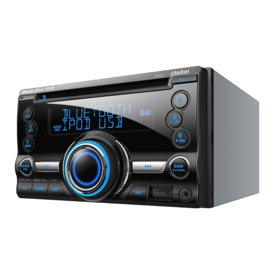
2-DIN Bluetooth CD/USB/MP3/
WMA RECEIVER
CX501
Model
(PE-3402B-A for USA )
CX501B
Model
(PE-3402B-B for BRAZIL )
CX501A
Model
(PE-3402K-A for Australia)
(PE-3402K-B for Asia)
Harmonic distortion:
MP3/WMA mode
MP3 Sampling rate:
MP3 Bit rate:
WMA Bit rate:
Logical format:
Bluetooth
Specification:
Profile:
Send/Receive Sensitivity:
Audio section
Maximum power output:
Bass control action:
Treble control action:
Line output level:
General
Power supply voltage:
Current consumption:
Speaker impedance:
Auto Antenna Rated Current: 500 mA or less
Weight:
Dimensions(mm):
Published by Service Dept.
298-6878-00 JAN.2011 P
Printed in P.R.C.
®
0.03%
8kHz to 48kHz
5kbps to 320kbps / VBR
5kbps to 320kbps
ISO9660 level1, 2
JOLIET or Romeo
Bluetooth Ver. 2.0+EDR
HSP(Headset Profile)
PBAP(Phone Book Access Profile)
HFP (Hands-Free Profile)
OPP (Object Push Profile) Phone
Book
A2DP (Advanced Audio Distribution
Profile)
AVRCP (Audio/Video Remote
Control Profile)
Class 2
50Wx4
+14/-14dB(100Hz)
+14/-14dB(10kHz)
4V(CD 1kHz) (PE-3402B-A)
2V(CD 1kHz)
(PE-3402B-B/PE3402K-A/B)
14.4V DC(10.8 to 15.6V allowable),
negative ground
Less than 15A
4ohm(4ohm to 8ohm allowable)
Source unit
1.52kg
Remote control unit 40g
(PE-3402B-A)
Source unit
178(W)x100(H)x155(D)
Remote control unit
44(W)x113(H)x11(D) (PE-3402B-A)
CX501/CX501B/CX501A
Advertisement
Table of Contents

Related Manuals for Clarion CX501


Summary of Contents for Clarion CX501
-
Page 1: Service Manual
Xiamen Clarion Electrical Enterprise Co., Ltd Published by Service Dept. 8/F., Xiamen Mail Processing Centre, No.275 Lujiang Road , Xiamen,China Tel:+86-592-2389080 Fax:+86-592-2389089 298-6878-00 JAN.2011 P Clarion Co., Ltd. Printed in P.R.C. 7-2, Shintoshin, Chuo-Ku, Saitama-Shi, Saitama 330-0081, Japan Service Manual ®... -
Page 2: To Engineers In Charge Of Repair Or Inspe- Ction Of Our Products
Bluetooth Please do not heat the chip capacitors with a soldering iron dire- SIG,Inc. and any use of such marks by Clarion Co.,Ltd. is under ctly. license. Other trademarks and trade names are those of their 7. -
Page 3: Error Displays
PE-3402K-A/B) 3-4. Spacer 340-1581-00 3-5. Double face 347-3913-20 4. Remote control unit(PE-3402B-A) RCB-176-600 Bottom view of PE-3402B-A FCC ID: WY2PE3402BA IC: 419E-CX501 Bluetooth QD ID: B017472 276-0793-00 (including battery CR2025) XXXXXXX PE-3402B MADE IN CHINA ERROR DISPLAYS If an error occurs, one of the following displays is displayed. Take the measures described below to eliminate the problem. -
Page 4: Troubleshooting
Can't insert the The device has been inserted Try reversing the connection direction of the device device. improperly. (usually the brand name surface should be facing left). The connector is broken. Replace with a new device. CX501/CX501B/CX501A... -
Page 5: Block Diagram
BLOCK DIAGRAM Main section PE-3402B-A PE-3402B-B/K-A/K-B KEY ILL LCD ILL CX501/CX501B/CX501A... - Page 6 0V level. : IN : ACC detection signal input. pin 71 : ACC-DET pin 42 : DVDD15 : IN : Capacitor connection pin for internal regulator. : IN : Backup detection signal input. pin 72 : B/U DET CX501/CX501B/CX501A...
- Page 7 10 : NC : IN : Not in use. pin 11 : PCM_IN : IN : Synchronous data input. pin 12 : PCM_SYNC : - : Synchronous data sync. pin 13 : PCM_CLK : - : Synchronous data clock. CX501/CX501B/CX501A...
-
Page 8: Exploded View Parts List
TRIM PLATE 075-9021-50 AUX JACK 345-5312-00 CUSHION 001-7062-90 DIODE 347-7321-00 E-SHEET 013-6312-50 TACT SWITCH 345-6422-00 SPONGE 076-0478-52 PLUG(2P) 716-0872-51 SPECIAL SCREW(M1.7x5) 074-3014-72 OUTLET SOCKET(22P) 382-9580-00 BUTTON(FW) ------------ SWITCH PWB1 382-9579-00 BUTTON(FF) ------------ SWITCH PWB2 335-9044-00 ILLUMI(MID) 076-0502-55 PLUG(5P)(PE-3402B-A/K-B) 347-8968-00 FILM CX501/CX501B/CX501A... - Page 9 855-2507-50 HD MINI DIN CORD 074-2215-60 OUTLET SOCKET(10P) 335-0833-01 LEAD HOLDER 074-3014-72 OUTLET SOCKET(22P) 311-1859-08 LOWER CASE ------------ MAIN PWB 854-4620-50 USB LEAD ------------ BT PWB 855-0642-50 USB CABLE ------------ MECH PWB 816-3063-55 FLAT WIRE 051-3730-00 331-4537-02 ES PLATE CX501/CX501B/CX501A...
-
Page 10: Electrical Parts List
187-1063-35 16V 10uF L206 010-4054-00 #886ANS-0904QH C211 166-3901-50 39pF CH C417 187-1063-35 16V 10uF L207 010-3072-90 560uH C212 168-2242-58 0.22uF B C418 187-1063-35 16V 10uF L208 010-3072-90 560uH C213 168-1042-78 16V 0.1uF C419 187-1063-35 16V 10uF L209 010-3105-62 1k ohm/100MHz CX501/CX501B/CX501A -10-... - Page 11 119-1031-15 1/10W 10k ohm R173 119-1031-15 1/10W 10k ohm R177 119-0000-05 1/10W 0 ohm JW R186 119-1031-15 1/10W 10k ohm R175 119-0000-05 R178 119-0000-05 1/10W 0 ohm JW R279 119-0000-05 1/10W 0 ohm JW 1/10W 0 ohm JW CX501/CX501B/CX501A -11-...
-
Page 12: Switch Pwb(B2) Section
D912 001-7088-92 HSMF-A355- P903 076-0478-52 2P R926 119-3311-15 1/10W 330 ohm G33J1 P904 076-0502-55 5P(PE-3402B-A R927 119-1031-15 1/10W 10k ohm D913 001-7088-92 HSMF-A355- /PE-3402K-B) R928 119-3311-15 1/10W 330 ohm G33J1 Q903 193-1781-50 2SC3440 R929 119-1031-15 1/10W 10k ohm CX501/CX501B/CX501A -12-... -
Page 13: Printed Wiring Board
043-1713-90 12pF R503 033-2731-15 1/10W 27k ohm R544 116-1501-15 1/4W 15 ohm C538 043-1713-90 12pF R504 033-8231-15 1/10W 82k ohm R545 116-1501-15 1/4W 15 ohm C539 043-1608-90 0.1uF R505 033-1241-15 1/10W 120k ohm R546 033-4701-15 1/10W 47 ohm CX501/CX501B/CX501A -13-... - Page 14 COMPONENT SIDE: Parts on the component side seen from the component side are indicated. To J503 of CD PWB(B4) (page 13) To J600 of BT PWB(B3) (page 15) Connect with FLAT WIRE 816-3063-55 To J901 of Switch PWB(B2) (page 16) CX501/CX501B/CX501A -14-...
- Page 15 To J301 of Main PWB(B1) (page 14) COMPONENT SIDE Caution: COMPONENT SIDE: Parts on the component side seen from the component side are indicated. SOLDER SIDE: Parts on the solder side seen from the solder side are indicated. CX501/CX501B/CX501A -15-...
-
Page 16: Circuit Diagram
COMPONENT SIDE: Parts on the component side seen from the component side are indicated. SOLDER SIDE: Parts on the solder side seen from the solder side are indicated. COMPONENT SIDE SOLDER SIDE To J301 of Main PWB(B1)(page 19) PE-3402B-A/K-B only PE-3402B-A/K-B only F-GND [ISR] [DISP] [SOUND] [SOURCE] CX501/CX501B/CX501A -16-... - Page 17 CIRCUIT DIAGRAM 2/7 PE-3402B-A Main PWB(B1) section 1/4 PE-3402B-B/K-A/K-B : To 2/4 (page 18) : To 3/4 (page 19) : To 4/4 (page 20) CX501/CX501B/CX501A -17-...
- Page 18 CIRCUIT DIAGRAM 3/7 Main PWB(B1) section 2/4 PE-3402B-A PE-3402B-B/K-A/K-B : To 1/4 (page 17) : To 3/4 (page 19) : To 4/4 (page 20) CX501/CX501B/CX501A -18-...
- Page 19 CIRCUIT DIAGRAM 4/7 Main PWB(B1) section 3/4 PE-3402B-A PE-3402B-B/K-A/K-B PE-3402B-A only PE-3402B-A only : To 1/4 (page 17) : To 2/4 (page 18) : To 4/4 (page 20) CX501/CX501B/CX501A -19-...
- Page 20 CIRCUIT DIAGRAM 5/7 Main PWB(B1) section 4/4 PE-3402B-A PE-3402B-B/K-A/K-B BACK : To 1/4 (page 17) : To 2/4 (page 18) : To 3/4 (page 19) CX501/CX501B/CX501A -20-...
- Page 21 CIRCUIT DIAGRAM 6/7 CD PWB(B4) section To PICK UP-ASSY CX501/CX501B/CX501A -21-...
- Page 22 CIRCUIT DIAGRAM 7/7 Switch PWB(B2) section [DISP] [ISR] ONLY FOR PE-3402B-A/PE-3402K-B [BAND] [ROTARY] [SOUND] CX501/CX501B/CX501A -22-...
-
Page 23: Service Material
SERVICE MATERIAL for PE-3402B-A / B-B / K-A / K-B...