Sony CDX-L510X Service Manual
Fm/am compact disc player
Hide thumbs
Also See for CDX-L510X:
- Service manual (46 pages) ,
- Operating instructions manual (40 pages) ,
- Installation/connections (5 pages)
Advertisement
Quick Links
Download this manual
See also:
Service Manual
SERVICE MANUAL
Ver 1.1 2003. 06
• The tuner and CD sections have no adjustments.
AUDIO POWER SPECIFICATIONS (US Model)
POWER OUTPUT AND TOTAL HARMONIC DISTORTION
23.2 watts per channel minimum continuous average power into
4 ohms, 4 channels driven from 20 Hz to 20 kHz with no more
than 5% total harmonic distortion.
CD player section
Signal-to-noise ratio
90 dB
Frequency response
10 – 20,000 Hz
Wow and flutter
Below measurable limit
Tuner section
FM
Tuning range
87.5 – 107.9 MHz
Antenna terminal
External antenna connector
Intermediate frequency 10.7 MHz
Usable sensitivity
11 dBf
Selectivity
75 dB at 400 kHz
Signal-to-noise ratio
65 dB (stereo),
68 dB (mono)
Harmonic distortion at 1 kHz
0.7% (stereo),
0.5% (mono)
Separation
33 dB at 1 kHz
Frequency response
30 – 15,000 Hz
AM
Tuning range
530 – 1,710 kHz
Antenna terminal
External antenna connector
Intermediate frequency 10.7 MHz/450 kHz
Sensitivity
AM: 30 µV
Power amplifier section
Outputs
Speaker outputs
(sure seal connectors)
Speaker impedance
4 – 8 ohms
Maximum power output 50 W × 4 (at 4 ohms)
Sony Corporation
9-874-231-02
2003F04-1
e Vehicle Company
© 2003. 06
Published by Sony Engineering Corporation
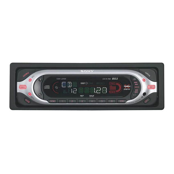
CDX-L510X
Model Name Using Similar Mechanism
CD Drive Mechanism Type
Optical Pick-up Name
SPECIFICATIONS
General
Outputs
Inputs
Tone controls
Power requirements
Dimensions
Mounting dimensions
Mass
Supplied accessories
Note
This unit cannot be connected to a digital preamplifier or an equalizer.
Design and specifications are subject to change without
notice.
FM/AM COMPACT DISC PLAYER
US Model
Canadian Model
CDX-L280
MG-393XC-121//K
KSS-721A
Audio outputs (rear)
Power antenna relay control terminal
Power amplifier control terminal
Remote controller input terminal
Antenna input terminal
Low: ±10 dB at 60 Hz (XPLOD)
Mid: ±10 dB at 1 kHz (XPLOD)
High: ±10 dB at 10 kHz (XPLOD)
12 V DC car battery
(negative ground)
Approx. 178 × 50 × 180 mm
× 2 × 7
(7
in.) (w/h/d)
1/8
1/8
Approx. 182 × 53 × 161 mm
× 2
× 6
(7
in.) (w/h/d)
1/4
1/8
3/8
Approx. 1.2 kg
(2 lb. 10 oz.)
Parts for installation and connections
Front panel case (1)
Card remote commander
RM-X115
1
Advertisement

Related Manuals for Sony CDX-L510X


Summary of Contents for Sony CDX-L510X
- Page 1 Speaker outputs (sure seal connectors) Speaker impedance 4 – 8 ohms Maximum power output 50 W × 4 (at 4 ohms) FM/AM COMPACT DISC PLAYER Sony Corporation 9-874-231-02 2003F04-1 e Vehicle Company © 2003. 06 Published by Sony Engineering Corporation...
-
Page 2: Block Diagram -Cd Section
CDX-L510X 3-3. BLOCK DIAGRAM — CD SECTION — RF AMP,DIGITAL SERVO DIGITAL SIGNAL PROCESSOR OPTICAL PICK-UP KSS-721A TUNER SECTION LOUT SYSTEM CONTROL ROUT IC801(1/3) CONV R-CH (Page 16) DEMOD PACK TSTB DSUB CODE TSCK PROCESS CONV. X_SO/PLL_SO FORCUS X_SI ERROR... -
Page 3: Block Diagram -Tuner Section
CDX-L510X 3-4. BLOCK DIAGRAM — TUNER SECTION — PJ401 REAR AUDIO OUT R-CH (Page 15) POWER AMP ELECTRONIC VOLUME IC101 IC401 CNP901 TUNER UNIT TU601 OUTF1 SECTION FL– CNJ601 FM_ANT L-CH (ANTENNA) R-CH R-CH OUTR1 AM_ANT DET_OUT RL– 16 AUX-IN... -
Page 4: Block Diagram -Display Section
CDX-L510X • Waveforms 3-5. BLOCK DIAGRAM — DISPLAY SECTION — — Servo Board — Main Board (MODE: CD PLAY) — — SYSTEM CONTROL LCD DRIVER IC801 (3/3) IC901 KEY 0 SEG1 2Vp-p KEY 0 5Vp-p KEY MATRIX LCD DO DATA... - Page 5 CDX-L510X • Refer to page 17 for Waveforms. 3-7. SCHEMATIC DIAGRAM — CD MECHANISM SECTION — • Refer to page 27 for IC Block Diagrams. TP77 TP78 TP89 TP79 TP80 TP81 TP82 TP45 TP10 TP83 TP44 TP43 TP84 TP42 TP41...
- Page 6 CDX-L510X 3-9. SCHEMATIC DIAGRAM — MAIN SECTION (1/2) — • Refer to page 17 for Waveforms. Q907 Q910 TH901 Q917 Q916 Q919 Q918 R914 R835 R930 R916 R933 Q906 (Page 23) R913 R934 D907 D809 R931 R932 R833 R832 Q929...
- Page 7 CDX-L510X • Refer to page 17 for Waveform. 3-10. SCHEMATIC DIAGRAM — MAIN SECTION (2/2) — • Refer to page 28 for IC Block Diagrams. CNP901 C901 D901 IC101 C401 C105 R105 JR411 PJ401 Q101 R109 C103 R107 R206 R401...
- Page 8 CDX-L510X 3-13. SCHEMATIC DIAGRAM — DISPLAY, RELAY SECTION — R972 R974 R976 R978 R980 R982 IC951 R966 R967 R940 R941 R951 LSW901(2/2) LSW914(2/2) LSW910(2/2) LSW918(2/2) LSW905(2/2) LSW902(2/2) R987 R984 C951 LED906 LED904 LSW912(2/2) LSW915(2/2) LSW909(2/2) LSW906(2/2) LED915 LED914 R952 R989...