Philips LX3600D Service Manual
Hide thumbs
Also See for LX3600D:
- Service manual (59 pages) ,
- Specifications (2 pages) ,
- Specification sheet (2 pages)
Table of Contents
Advertisement
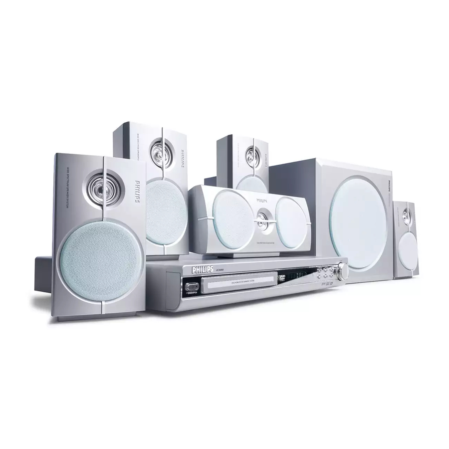
DVD Receiver
Service
Service
Service
Service
Service
Service Manual
©
Copyright 2003 Philips Consumer Electronics B.V. Eindhoven, The Netherlands
All rights reserved. No part of this publication may be reproduced, stored in a retrieval system or
transmitted, in any form or by any means, electronic, mechanical, photocopying, or otherwise
without the prior permission of Philips.
Published by KC 0327 Service Audio
Version 1.1
TABLE OF CONTENTS
Location Of Pc Boards & Version variations ................ 1-2
Technical Specifications ............................................. 1-3
Measurement Setup .................................................... 1-4
Service Aids, Safety Instruction, etc. ......................... 1-5
Disassembly Instructions & Service positions ........... 2-1
Service Test Program ................................................. 3-1
Region code, Software version & upgrades ............... 3-2
Set Block Diagram & Wiring diagram ............................ 4
Psu Board ( For info only ) .............................................. 5
Front Board .................................................................... 6
Mono AV Board .............................................................. 7
Amplifier Board .............................................................. 8
Speaker Connector Board ............................................. 9
Set Mechanical Exploded view & parts list ................. 10
History .......................................................................... 11
Printed in The Netherlands
Subject to modification
LX3600D/
17/22/25/69/75/78
Page
CLASS 1
LASER PRODUCT
GB
3139 785 30371
Advertisement
Table of Contents

Related Manuals for Philips LX3600D


Summary of Contents for Philips LX3600D
- Page 1 LASER PRODUCT © Copyright 2003 Philips Consumer Electronics B.V. Eindhoven, The Netherlands All rights reserved. No part of this publication may be reproduced, stored in a retrieval system or transmitted, in any form or by any means, electronic, mechanical, photocopying, or otherwise without the prior permission of Philips.
-
Page 2: Location Of Pc Boards
LOCATION OF PC BOARDS VERSION VARIATIONS: Type /Versions: LX3600D Features & Board in used: Progressive Scan Voltage Selector Aux-In TV-In Line-Out Composite (CVBS) Output S-Video Output Component (Pr/Y/Pb) Outputs SCART Output Production start-up with 220-240V PSU before changeover to PSU with voltage selector... - Page 3 SPECIFICATIONS Output sensitivity GENERAL: Line out : 700mV ± 2dB at 47kΩ Mains voltage : 120V for /17 Scart-out : 600mV ± 2dB at 10kΩ 220-240V for /22/25/75 110-127V/220-240V Switchable for /69/78 COMPACT DISC/VCD/DVD: Mains frequency : 50/60Hz Video Decoding : MPEG-2 / MPEG-1 Power consumption : <...
-
Page 4: Measurement Setup
MEASUREMENT SETUP Tuner FM Bandpass LF Voltmeter 250Hz-15kHz e.g. PM2534 e.g. 7122 707 48001 RF Generator e.g. PM5326 S/N and distortion meter e.g. Sound Technology ST1700B Use a bandpass filter to eliminate hum (50Hz, 100Hz) and disturbance from the pilottone (19kHz, 38kHz). Tuner AM (MW,LW) Bandpass LF Voltmeter... - Page 5 SERVICE AIDS Service Tools: Universal Torx driver holder ........4822 395 91019 Torx bit T10 150mm ..........4822 395 50456 Torx driver set T6 - T20 ......... 4822 395 50145 Torx driver T10 extended ........4822 395 50423 Compact Disc: SBC426/426A Test disc 5 + 5A ......
- Page 6 WAARSCHUWING WARNING Alle IC’s en vele andere halfgeleiders zijn All ICs and many other semi-conductors are gevoelig voor electrostatische ontladingen (ESD). susceptible to electrostatic discharges (ESD). Onzorgvuldig behandelen tijdens reparatie kan Careless handling during repair can reduce life de levensduur drastisch doen verminderen. drastically.
-
Page 7: Dismantling Instructions
DISMANTLING INSTRUCTIONS Dismantling of the Front Panel assembly 1) Open the Tray and remove the tray cover assy (pos 5 + 2) Loosen the 5 screws to dismantle the Top Cover (pos 7) and remove it as shown in figure 1. 252) - 2 screws on each side Note: The Tray can be manually open by inserting a... - Page 8 Service positions Mono AV board Amplifier board Thick insulation sheet or paper Thick insulation sheet or paper Speaker Connector board Thick insulation sheet or paper...
-
Page 9: Service Test Program
SOURCE / VOLUME Display shows value for 2 seconds. Knob Values increases or decreases in steps of 1 until ENCODER TEST 0 (Min.) or 40 (Max.) is reached. Disconnect LEAVE SERVICE mains cord TEST PROGRAM LX3600D Service Test Program dd wk0326... - Page 10 - UPG END [only for a short moment, if unsuccessful ERROR is displayed] <9> <9> <9> <9> <AUDIO> <5> .. for LX3600D India Kit <9> <9> <9> <9> <AUDIO> <7> . for LX3600D Brazil Kit - DISC - LOAD [Tray will close indicating that the upgrade <9>...
- Page 11 SET BLOCK DIAGRAM TDA8920 74HC4052 POWER AMP TDA8920 TUNER (TM 08) SURROUND POWER AMP 1/2xTDA8920 1/2XTDA8920 LX3600D/22 Block Diagram ..37121 dd wk334.5...
- Page 12 3139 110 34581 EH 11P PH 9P FFC, 0.5mm pitch EH 10P 120mm 120mm 140mm 3139 111 01751 3139 110 28081 100mm 140mm 100mm 140mm FFC BD 11p 100mm 100mm 3139 110 35910 LX3600D/22 Set Wiring ...37110 dd wk334.5 220mm...
- Page 13 PSU BOARD (For Information only) It is not recommended for component repair on this board but to replace the board when it becomes defective. Therefore no service parts list is published in this chapter. The only service part available for replacement is: PSU Board 220V-240V ........
- Page 14 PSU CIRCUIT 1 - 220-240V version (FOR INFORMATION ONLY) I130 1101 F101 F102 5100 F105 F106 VALUE 90Mhz 700R 6105 6106 B2P-VA-BF 1N4006 1N4006 F109 2140 6107 6108 1100 HF2430 1N4006 1N4006 3100 5101 I201 5200 F103 F104 F108 F205 F206 F207 F208...
- Page 15 PSU CIRCUIT 2 - 220-240V version (FOR INFORMATION ONLY) 2220 2190 470p I250 I251 I252 5220 F220 F221 6220 7220 +12VA 5190 BYV27-200 CT282D4 BC327-25 3123 0201 EH-B 3221 7221 +5VDstby BC847B +5VDstby +5VL I256 I257 I258 5280 F280 F281 6280 +12VA -12VA...
- Page 16 PSU CIRCUIT 1 - Voltage Selector version (FOR INFORMATION ONLY) I130 1101 5100 F101 F102 F105 F106 90Mhz 700R VALUE 6105 6106 B2P-VA-BF 1N4006 1N4006 F109 2140 6107 6108 1100 HF2430 1N4006 1N4006 1102 3100 5101 I201 5200 F103 F104 F108 F119 F112...
- Page 17 PSU CIRCUIT 2 - Voltage Selector version (FOR INFORMATION ONLY) 2220 2190 470p +5VDstby I250 I251 I252 5220 F220 F221 6220 7220 +12VA 5190 BYV27-200 CT282D4 BC327-25 +5VDstby +5VL 3123 0201 EH-B I112 +12VA 3221 7221 BC847B -12VA I256 I257 I258 5280 F280...
- Page 18 PSU CIRCUIT 1 - 120V version (FOR INFORMATION ONLY) I130 1101 F101 F102 5100 F105 F106 VALUE 90Mhz 700R 6105 6106 B2P-VA-BF 1N4006 1N4006 F109 2140 6107 6108 1100 HF2430 1N4006 1N4006 3100 5101 I201 5200 F103 F104 F108 F119 F112 F113 F205...
- Page 19 PSU CIRCUIT 2 - 120V version (FOR INFORMATION ONLY) 2220 2190 470p +5VDstby I250 I251 I252 5220 6220 F220 F221 7220 +12VA 5190 BYV27-200 CT282D4 BC327-25 +5VDstby +5VL 3123 0201 EH-B I112 +12VA 3221 7221 BC847B -12VA I256 I257 I258 5280 6280 F280...
- Page 20 FTD DISPLAY PIN CONNECTIONS FRONT BOARDS TABLE OF CONTENTS (1G-7G) FTD Display pin connection ................. 6-1 Front Standby part - circuit & layouts ............6-2 Front Display part - Circuit diagram ............. 6-3 Front Display part - Component & Chip layouts .......... 6-4 Front Display part - Chip layout Part A ............
- Page 21 FRONT STANDBY PART - CIRCUIT DIAGRAM FRONT STANDBY PART - COMPONENT & CHIP LAYOUT 1201 A1 2201 B2 3202 A2 6201 A2 7201 A2 1202 B2 3201 A2 3203 B2 6202 B2 +5VDSTBY FE-BT-VK-N 1201 7201 BC847B 3202 POWER_ON STB_SW STANDBY 8239 210 9630 pt3 dd wk0325 8239 210 9630 pt3 dd wk0325...
-
Page 22: Display Board
FRONT DISPLAY PART - CIRCUIT DIAGRAM 1100 A5 1103 E5 1106 E4 1111 D2 2101 C2 2104 F2 2107 C9 2110 E9 2113 F9 2116 B2 2119 C2 2122 C3 3101 E1 3104 D3 3107 C4 3110 B4 3113 F5 3117 E8 3120 F7 3123 F9... - Page 23 FRONT DISPLAY PART - COMPONENT & CHIP LAYOUT This assemby drawing shows a summary of all possible versions. For components used in a specific version see schematic and respective parts list. 8239 210 9625 pt3 dd wk0325 This assemby drawing shows a summary of all possible versions. For components used in a specific version see schematic and respective parts list. PART A PART B 8239 210 9625 pt3 dd wk0325...
- Page 24 FRONT DISPLAY PART - CHIP LAYOUT PART A This assemby drawing shows a summary of all possible versions. For components used i PART A...
- Page 25 FRONT DISPLAY PART - CHIP LAYOUT PART B ts used in a specific version see schematic and respective parts list. PART B 8239 210 9625 pt3 dd wk0325...
- Page 26 ELECTRICAL PARTS LIST - FRONT BOARDS MISCELLANEOUS 3122 4822 051 30472 4k7 5% 0,062W 1100 3141 010 50311 VFD Display HNV-07SS54T 1101 4822 265 11515 Flex Socket 8P Vert 3123 4822 051 30103 10k 5% 0,062W 1103 4822 276 13775 Tact Switch 3125 4822 051 30103...
- Page 27 CS5333 Internal Block diagram VA VL AINL LP Filter Digital Decimation Filter Comparator SDATA LRCK SCLK AV BOARD LP Filter AINR Digital Decimation Filter Comparator MCLK FILT+ REF_GND TABLE OF CONTENTS M29W160ET Internal Block diagram CS5333 & M29W160ET Internal Block diagram ....... 7-1 Reset, Power Supply &...
- Page 28 DV33 220u 3533 2782 10u 50V 7501 3530 NCP303LSN30 URST 2 INP 5604 OUTP 7502 AVCC NC RESET BC847B 3611 6605 2609 2786 100n 220u 10V 2513 100n LX3600D Mono AV 3139 113 3522 pt 1 Circuit 1 dd wk334...
- Page 29 7602 D9 1712 3647 3645 7603 D2 TROPEN V1P4 RVCCIN RVCCIN 7620 B4 7621 B2 7630 A2 TRIN 7631 A3 7632 A3 TROUT 7604 I2 LOAD+ LOAD- B9B-PH-K LX3600D Mono AV 3139 113 3522 pt 1 Circuit 2 dd wk334...
- Page 30 4579 F13 DV33 5626 5613 3669 3671 DV33 5610 F13 5613 I11 VSTB 5625 A1 3534 5626 I1 VSDA 3739 5701 B12 +5VL 7500 F12 7605 A12 LX3600D Mono AV 3139 113 3522 pt 1 Circuit 3 dd wk334 7606 E6...
- Page 31 Φ 2 BICK 3723 PCM_CLK AOUTR+ ROUT+ (2Kx8) 3 SDTI PCM_LTRT AOUTR- 9 2703 EEPROM INTERPOLATOR ROUT- 100n DV33_F PWR# PRD# VRST PCE# BYTE 2509 GND_A 100n GND_A LX3600D Mono AV 3139 113 3522 pt 1 Circuit 4 dd wk334...
- Page 32 0 - 2V : Output on 0_6_12 TV BCAST 3818 4.5 - 7V : 16 : 9 DVD 3817 7654 SCART1 4: 3 DVD BC847B 9.5-12V : 3816 LX3600D Mono AV 3139 113 3522 pt 1 Circuit 5 dd wk334...
- Page 33 3177 3178 3115 I5 7102 PW_DN GND_C 3120 A9 A_HP BC547B 330p 470p +12VL 3121 B10 GND_C 3122 B10 AGND 3123 A10 3124 B10 3125 B10 3126 B12 LX3600D Mono AV 3139 113 3522 pt 1 Circuit 6 dd wk334...
- Page 34 GND_A 3271 LPR6520-K410G COAXL 3268 B6 3269 E8 3270 E9 3271 I3 1203 3272 B11 3273 B12 3274 B11 GND_A 3290 C10 4200 F10 4201 F10 LX3600D Mono AV 3139 113 3522 pt 1 Circuit 7 dd wk334 4202 F11...
- Page 35 220p 3375 H10 3378 3376 H9 VOL_A 3377 H10 1308 3378 H9 GND_C GND_C FE-BT-VK-N 4310 A5 4315 A5 GND_C 4316 G4 4317 G4 6310 A5 6351 F7 LX3600D Mono AV 3139 113 3522 pt 1 Circuit 8 dd wk334...
- Page 36 7-10 7-10 PCB 3139 113 3520 pt3 TOP VIEW - Use by LX3600D/22 & /25 only (during production start-up) This assembly drawing shows a summary of possible version. For components used in aspecific versions see schematic and respective parts list.
- Page 37 7-11 7-11 PCB 3139 113 3520 pt3 TOP VIEW MAPPING (For Page 7-10 only) 2601 C6 2791 D6 3257 F12 3623 D9 3724 E10 5607 C8 1101 C2 2167 G4 2673 C6 7631 C9 2610 D9 2793 E3 3258 F11 3624 D9 3727 E12 5608 C8...
- Page 38 7-12 7-12 PCB 3139 113 3520 pt3 BOTTOM VIEW - Use by LX3600D/22 & /25 only (during production start-up) This assembly drawing shows a summary of possible version. For components used in aspecific versions see schematic and respective parts list.
- Page 39 7-13 7-13 PCB 3139 113 3520 pt3 BOTTOM VIEW MAPPING (For Page 7-12 only) 2218 F3 2517 F5 2816 F6 3174 G11 3266 G12 3604 C9 4562 F9 6625 2101 E8 2219 F3 2603 D11 2817 G5 3175 F12 3269 F4 3606 C10 4563 F9 6626...
- Page 40 PCB 3139 113 3522 pt1 TOP VIEW - Use by all type/versions This assembly drawing shows a summary of possible version. For components used in aspecific versions see schematic and respective parts list. LX3600D/69 3139 113 3522 pt1 dd wk341...
- Page 41 7-15 7-15 PCB 3139 113 3522 pt1 TOP VIEW MAPPING (For Page 7-14 only) 1101 C2 2158 G5 2384 F3 2649 C4 2764 C11 3148 G5 3353 F2 3652 E7 3796 G10 5701 E7 7653 H9 1104 G2 2163 G3 2387 C12 2653 E7 2765 D12...
- Page 42 PCB 3139 113 3522 pt1 BOTTOM VIEW - Use by all Type/versions This assembly drawing shows a summary of possible version. For components used in aspecific versions see schematic and respective parts list. LX3600D/69 3139 113 3522 pt1 dd wk341...
- Page 43 7-17 7-17 PCB 3139 113 3522 pt1 BOTTOM VIEW MAPPING (For Page 7-16 only) 2101 E8 2195 C13 2351 G8 2659 D8 2820 G6 3163 G11 3242 E4 3365 F12 3633 B12 4565 6603 2107 F8 2196 C13 2361 E13 2661 E9 2821 G7 3164 G11...
- Page 44 7-18 7-18 ELECTRICAL PARTS LIST - MONO AV BOARD ELECTRICAL PARTS LIST - MONO AV BOARD MISCELLANEOUS 1102 3139 241 21102 EMC Spring 2150 4822 126 14241 330pF 50V 2223 2020 552 96305 4,7uF +80/-20% 10V 2386 2238 586 59812 100nF +80/-20% 50V 1103 3139 241 21102...
- Page 45 7-19 7-19 ELECTRICAL PARTS LIST - MONO AV BOARD ELECTRICAL PARTS LIST - MONO AV BOARD CAPACITORS 2638 3198 017 41050 1uF 10V 2699 2238 586 59812 100nF +80/-20% 50V 2794 4822 124 40196 220uF 20% 16V 3146 4822 051 30103 10k 5% 0,062W 2639 3198 017 41050...
- Page 46 7-20 7-20 ELECTRICAL PARTS LIST - MONO AV BOARD ELECTRICAL PARTS LIST - MONO AV BOARD RESISTORS 3219 4822 117 13632 100k 1% 0,062W 3315 4822 117 13632 100k 1% 0,062W 3524 4822 051 30151 150R 5% 0,062W 3655 4822 051 30183 18k 5% 0,062W 3220 4822 051 30151...
- Page 47 7-21 7-21 ELECTRICAL PARTS LIST - MONO AV BOARD ELECTRICAL PARTS LIST - MONO AV BOARD RESISTORS COILS & FILTERS 3793 4822 051 30008 0R Jumper 0603 5100 3198 018 63390 Coil 33uH 5% 1008 6609 4822 130 11522 BZX384-C15 7618 4822 130 60373 BC857B...
- Page 48 6-channel class-D amplifier Basic operation of a class-D amplifier Basically, the output stage of a class-D amplifier outputs a continuous square wave swinging between positive and negative power supplies with a fixed frequency (“clock” frequency) far beyond the audible range. The duty cycle of this square wave is modulated with the audio signal. The output is followed by a low-pass filter which eliminates the clock frequency and allows only the audio signal going to the speaker.
- Page 49 MECHANICAL EXPLODED VIEW Block diagram and operation SINGLE ENDED 6 x 75W BRIDGE 3 x 100W TDA8920 TDA8920 output 1 input 1 output 1 input 1 input 2 output 2 TDA8920 TDA8920 output 2 input 3 output 3 input 2 input 4 output 4 TDA8920...
- Page 50 AMPLIFIER CIRCUIT 1306 A7 5203 F5 1307 H7 5302 H5 1308 E7 5303 I5 1316 B7 7100 A2 2106 1317 I7 7200 D2 1318 E7 7300 H2 2104 2107 2101 A3 2102 A3 100n 100n 2104 A4 2101 +28V 2102 2105 2108 2105 A4...
- Page 51 CLOCK GENERATOR & CONNECTOR CIRCUIT 1301 B1 7716 I12 1302 B2 1303 E2 1304 G2 1305 E1 1309 G1 1312 G3 1320 I5 1400 I6 1600 E9 3414 INPUT_1 1601 G9 3415 2400 H3 INPUT_2N 2401 H4 3416 INPUT_3 MODE_12 2402 H4 2403 H3 3417...
- Page 52 BOTTOM VIEW LAYOUT This assemby drawing shows a summary of all possible versions. For components used in a specific version see schematic and respective parts list. PART A PART B 3139 113 3530 pt1 dd wk0340...
- Page 53 TOP VIEW LAYOUT This assemby drawing shows a summary of all possible versions. For components used in a specific version see schematic and respective parts list. PART C PART D 3139 113 3530 pt1 dd wk0340...
- Page 54 BOTTOM VIEW LAYOUT - PART A This assemby drawing shows a summary of all possible versions. For components used in a specific version see schematic and respective parts list. PART A...
- Page 55 BOTTOM VIEW LAYOUT - PART B PART B 3139 113 3530 pt1 dd wk0340...
- Page 56 TOP VIEW LAYOUT - PART C This assemby drawing shows a summary of all possible versions. For components used in a specific version see schematic and respective parts list. PART C...
- Page 57 8-10 8-10 TOP VIEW LAYOUT - PART D PART D 3139 113 3530 pt1 dd wk0340...
- Page 58 8-11 ELECTRICAL PARTS LIST - AMPLIFIER BOARD MISCELLANEOUS 2229 2222 580 15649 100nF 10% 50V 3104 211 29861 Spring 6-Channel 2230 2222 580 15649 100nF 10% 50V 3104 211 29881 Earth Spring 2231 4822 126 14241 330pF 50V 1302 4822 267 10729 Flex Socket 10P Vert.
- Page 59 8-12 ELECTRICAL PARTS LIST - AMPLIFIER BOARD CAPACITORS 2421 5322 126 11578 1nF 10% 50V 3305 4822 051 10568 5R6 5% 0,25W 2422 5322 126 11578 1nF 10% 50V 3307 4822 051 30109 10R 5% 0,062W 2423 2238 586 59812 100nF +80/-20% 50V 3309 4822 051 30109...
- Page 60 8-13 ELECTRICAL PARTS LIST - AMPLIFIER BOARD DIODES 6600 3198 020 55680 BZX384-C5V6 6713 4822 130 11397 BAS316 6714 4822 130 11397 BAS316 6715 4822 130 11397 BAS316 TRANSISTORS & INTEGRATED CIRCUITS 7100 9352 705 74518 TDA8920TH/N1 7200 9352 705 74518 TDA8920TH/N1 7300 9352 705 74518...
- Page 61 ELECTRICAL PARTS LIST - SPEAKER CONNECTOR BOARD MISCELLANEOUS 1711 2422 025 18178 Speaker Socket 6P Pur/Blue/Gry 1712 2422 025 18179 Speaker Socket 6P Wte/Grn/Red CAPACITORS 2202 5322 126 11583 10nF 10% 50V 2203 5322 126 11583 10nF 10% 50V 2204 5322 126 11583 10nF 10% 50V 2205...
- Page 62 CIRCUIT DIAGRAM 0011 C1 0012 D1 0013 A1 1711 D6 1712 A7 2202 A4 2203 A4 2204 B4 2205 B4 0013 2206 C4 2202 2207 C4 LQR3315-1101G 2208 C5 2209 D5 1712 2203 2210 D4 2211 D4 2212 E5 TO AMP 2213 E5 BOARD 2204...
- Page 63 COMPONENT LAYOUT CHIP LAYOUT...
- Page 64 10-1 MAIN ENCASING EXPLODED VIEW (For /22 & 125 only)
- Page 65 10-2 MAIN ENCASING EXPLODED VIEW (For all versions except /22 & /25)
- Page 66 10-3 FRONT CABINET ASSY EXPLODED VIEW Cabinet Front Assy 3139 257 51330 dd wk330 BOTTOM PLATE ASSY EXPLODED VIEW Plate Bottom assy 3139 257 51340 dd wk341...
- Page 67 3139 257 51221 Cabinet Front /22/25 D3 x 8 3139 257 51411 Cabinet Front /69/75/78 3139 247 51831 Badge Philips Silver D3 x 8 M3 x 6 3139 257 51231 Button Power/Standby M3 x 6 3139 114 79541 Lightguide Standby...
- Page 68 Initial release Version 1.1 Modify/Add the undermentioned pages to include LX3600D/17, /69, /75 and /78: Pages: 1-1 to 1-3, 3-2, 4-1 to 4-2, 5-1, 5-4 to 5-7, 7-2 to 7-17, and 10-1 to 10-4 Note: In Chapter 7 - new pcb 3139 113 3522 pt 1 is added to replcace the existing board that does not support the new type/version.