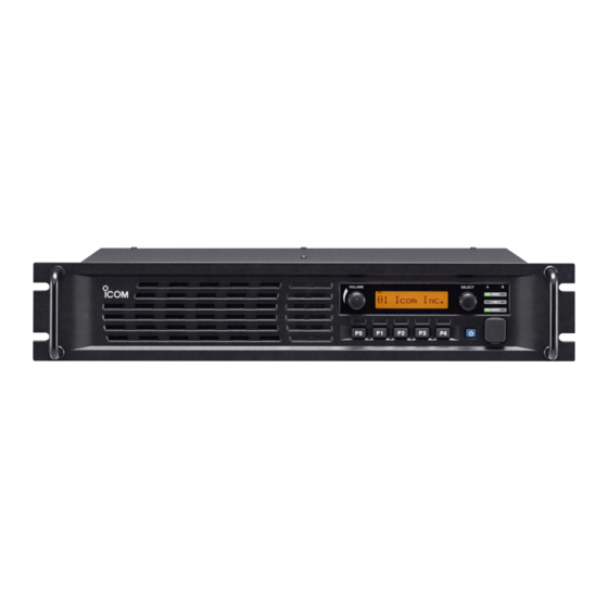
Icom IC-FR5000 Service Manual
Vhf fm repeater
Hide thumbs
Also See for IC-FR5000:
- Service manual addendum (181 pages) ,
- Insrtuction manual (16 pages) ,
- Instruction manual (16 pages)
Table of Contents
Advertisement
Advertisement
Table of Contents

Related Manuals for Icom IC-FR5000


Summary of Contents for Icom IC-FR5000
- Page 1 VHF FM REPEATER S-14425XZ-C1 Jun. 2008...
- Page 2 8. READ the instructions of test equipment throughly before connecting a test equipment to the repeater. Icom, Icom Inc. and logo are registered trademarks of Icom Incorporated (Japan) in the United States, the United Kingdom, Germany, France, Spain, Russia and/or other countries.
-
Page 3: Table Of Contents
CONTENTS SECTION SPECIFICATIONS SECTION INSIDE VIEWS SECTION DISASSEMBLY INSTRUCTION SECTION OPTIONAL UNIT INSTALLATION SECTION CIRCUIT DESCRIPITON RECEIVER CIRCUITS............5-1 TRANSMITTER CIRCUITS . -
Page 4: Specifications
SECTION 1 SPECIFICATIONS GENERAL [FR5000] [FR5100] • Frequency coverage 136–174 MHz • Conventional channels max. 32 ch • Type of emission Wide 16K0F3E Middle – 14K0F3E Narrow 11K0F3E/11K0F7E/11K0F7D/11K0F7W/ 8K50F3E 8K50F3E ([EXP-01] only) Digital 4K00F1E/4K00F1D/4K00F3E 50 Ω (Nominal) • Antenna impedance •... - Page 5 RECEIVER [FR5000] [FR5100] • Receive system Double-conversion superheterodyne system • Intermediate frequencies 1st IF: 46.35 MHz, 2nd IF: 450 kHz 0.3 μV typ. at 12 dB SINAD • Sensitivity Wide/Narrow –10 dBμV max. at 12 dB SINAD Wide/Middle/Narrow – –10 dBμV max. at 12 dB SINAD 0.25 μV typ.
-
Page 6: Section 2 Inside Views
SECTION 2 INSIDE VIEWS D/A converter (IC20) • MAIN UNIT (TOP VIEW) 5V regulator (CPU5V) (IC30) Power SW (VCC line) (Q57) Level converter (IC26) 8V regulator (8V line) Optional digital unit slot (IC27) 8V regulator (T8V line) CPU clock (Q45) (X5) 5V regulator (+5V line) (Q41) - Page 7 • FRONT UNIT AF POWER AMP. (IC509) SPEAKER SW (Q508) ANALOG SW (IC506) LCD DRIVER (IC500) FRONT CPU (IC503) CLOCK OSC (X501) 2 - 2...
-
Page 8: Section 3 Disassembly Instruction
SECTION 3 DISASSEMBLY INSTRUCTION 1. Removing the front panel q Unscrew 11 screws from the top cover. w Unscrew 7 screws from the front panel. e Disconnect the cable from the MAIN UNIT assembly, and remove the front panel. 2. Removing the MAIN UNIT assembly q Uscrew 5 screws which settles the MAIN UNIT assembly. - Page 9 w Unsolder 2 points at the ANT cases. e Unscrew 4 screws from the ANT cases, Unsolder and remove them. ANT case r Disconnect the flat cabe from J4 and the speaker cable from J9. Unscrew ANT case Flat cable Disconnect t Unsolder 2 points at the bottom of ANT connectors.
-
Page 10: Section 4 Optional Unit Installation
SECTION 4 OPTIONAL UNIT INSTALLATION Install UT-109R or UT-110R as follows. q Disassembly the repeater until the MAIN UNIT is exposed. (See the page 3-1) w Modify the patterns on the MAIN UNIT as below. <MAIN UNIT (bottom side)> A and F; Cut the pattern B;... -
Page 11: Receiver Circuits
SECTION 5 CIRCUIT DESCRIPTION 5-1 RECEIVER CIRCUITS 5-2 TRANSMITTER CIRCUITS RF BPF CIRCUITS MODULATION CIRCUITS RX signals from the RX antenna connector (J11) are passed The demodulated signals are applied to the MIC AMP (IC25). through the 1st stage of BPF (D28, 29, 31, 32, L44, 47) then The amplified Demodulated signals are passed through the amplified by the RF AMP (Q36). -
Page 12: Other Circuits
5-3 FREQUENCY SYNTHESIZER CIRCUITS 5-4 OTHER CIRCUITS RX PLL CIRCUIT POWER SUPPLY The RX PLL IC (IC4) outputs resulting signal; phase-comparison The power supply is switched by Q57 (ON/OFF). 5V (REF5) of reference signal (15.3 MHz) from the TCXO (X2) and fedback from the regulator (IC30) is passed through L58 to supply to OSC signal from the RX VCO. -
Page 13: Cpu (M: Ic20) Port Allocation
5-5 CPU (M: IC20) PORT ALLOCATION LINE NAME DESCRIPTION CONDITION 1–11 D5–D15 DSP data bus line. – 15–28 A1–A14 DSP data bus line. – DSP data line. – FANS Cooling fan (CH: MF1) rotation detect. "H"=While the cooling fan is rotating. TLED TX indicator LED control signal. - Page 14 5-5 CPU (M: IC20) PORT ALLOCATION (continued) LINE NAME DESCRIPTION CONDITION DAST Strobe to the DAC (M: IC2). – FMDA Data from the FRONT CPU (F: IC502). – MFDA Data to the FRONT CPU (F: IC502). – OPT2 Port for optional unit. –...
-
Page 15: Preparation
SECTION 6 ADJUSTMENT PROCEDURE 6-1 PREPARATION ¤ REQUIRED EQUIPMENTS EQUIPMENT SPECIFICATION EQUIPMENT SPECIFICATION Adjustment Modifi ed OPC-1122U (USB type) "CS-FR5000" (Revision 1.0 or later) JIG cable Software (see the illust below) Output voltage : 13.6 V DC [FR5000] Power attenuation : 40 dB 13.2 V DC [FR5100] Capacity : More than 60 W... - Page 16 ¤ CONNECTION <Rear view> OSCILLOSCOPE MODULATION ANALYZER (DC to 10 kHz) (0.1–300 MHz) ATTENUATOR STANDARD SIGNAL GENERATOR (30 dB/60 W) 20 A (0.1–300 MHz) fuses (Detect output) FREQUENCY COUNTER (0.1–300 MHz) RF POWER METER (Loose Coupling) DC power supply Black DC power cable 6 - 2...
- Page 17 ¤ ADJUSTMENT CHANNEL LISTS Clone the adjust channels into the repeater before starting adjustment. Each channel must be assigned [Frequency], [RF PWR], [CH Type], [TX C. Tone] and [W/N] as below. • Channel list 6 - 3...
- Page 18 ¤ WHOLE PROCEDURE OF THE ADJUSTMENT q Connect the repeater and PC with the JIG cable (see the page 6-2). w Turn the repeater power ON. e Boot up 'CS-FR5000.' r Set the [Digital Function] to "Enable." t Click or [Read <– TR] in the [Adjust] menu, then the "Adjust Utility" window (see the page 6-5) appears. y Set or modify adjustment values as specifi...
- Page 19 ¤ ADJUST UTILITY WINDOW Mode setting TX output power Analog deviation CTCSS/DTCS deviation Squelch TX frequency Lock volatge (Preset) Lock volatge (Adjustment) S-meter Modulation balance Modulation balance (High) Digital deviation Receive sensitivity (Band center) Receive sensitivity (Band high) 6 - 5...
-
Page 20: Frequency Adjustment
6-2 FREQUENCY ADJUSTMENT 1) Select an adjustment item using cursor or [↑] / [↓] keys of the PC’s keyboard. 2) Set or modify the adjustment value as specifi ed using [←] / [→] keys of the PC’s keyboard, then push the [ENTER] key. ADJUSTMENT ADJUSTMENT ADJUSTMENT CONDITION... -
Page 21: Transmit Adjustment
6-3 TRANSMIT ADJUSTMENT 1) Select an adjustment item using cursor or [↑] / [↓] keys of the PC’s keyboard. 2) Set or modify the adjustment value as specifi ed using [←] / [→] keys of the PC’s keyboard, then push the [ENTER] key. ADJUSTMENT ADJUSTMENT ADJUSTMENT CONDITION... -
Page 22: Receive Adjustment
6-3 TRANSMIT ADJUSTMENT (continued) 1) Select an adjustment item using cursor or [↑] / [↓] keys of the PC’s keyboard. 2) Set or modify the adjustment value as specifi ed using [←] / [→] keys of the PC’s keyboard, then push the [ENTER] key. ADJUSTMENT ADJUSTMENT ADJUSTMENT CONDITION... - Page 23 6-4 RECEIVE ADJUSTMENT (continued) 1) Select an adjustment item using cursor or [↑] / [↓] keys of the PC’s keyboard. 2) Set or modify the adjustment value as specifi ed using [←] / [→] keys of the PC’s keyboard, then push the [ENTER] key. ADJUSTMENT ADJUSTMENT ADJUSTMENT CONDITION...
-
Page 24: Front Unit
SECTION 7 PARTS LIST [FRONT UNIT] [FRONT UNIT] ORDER ORDER DESCRIPTION DESCRIPTION LOCATION LOCATION IC500 1130009121 S.IC S1D15206F00A200 69.4/35.9 R568 7030005050 S.RES ERJ2GEJ 103 X (10 k) 87.4/16.9 IC501 1110005771 S.IC S-80942CNMC-G9CT2G 105.3/24 R570 7030005220 S.RES ERJ2GEJ 223 X (22 k) 103/24.8 IC502 1140014580 S.IC... - Page 25 [FRONT UNIT] [MAIN UNIT] ORDER ORDER DESCRIPTION DESCRIPTION LOCATION LOCATION S506 2250000511 ECR RH70N1037E20-13F-2781 1110005330 S.IC NJM12904V-TE1-#ZZZB 58.1/71.4 1110007290 S.IC AK2330P-L 58.7/56.1 1130010100 S.IC LMX2352TMX/NOPB 120.2/43.9 SP501 2510001221 SP C052SB500-14 1130010100 S.IC LMX2352TMX/NOPB 28/78.8 1110003491 S.IC TA31136FNG (D,EL) 70.4/82.5 1110007280 S.IC NJM2716F-TE1-#ZZZB 56.8/46.4 W501...
- Page 26 [MAIN UNIT] [MAIN UNIT] ORDER ORDER DESCRIPTION DESCRIPTION LOCATION LOCATION 1750001070 S.DIO DAN235ETL 57.3/78.6 6200007120 S.COL ELJND 1R0J 28.7/116.8 1750001070 S.DIO DAN235ETL 50/79.7 6200009910 S.COL C6342A-88NG-A 88.8/63.9 1790001621 S.DIO 1SV308 (TPL3,F) 69.3/94.8 6200007120 S.COL ELJND 1R0J 83.5/66.4 1790001621 S.DIO 1SV308 (TPL3,F) 69.3/92.2 6200007120 S.COL ELJND 1R0J 30.2/124.7...
- Page 27 [MAIN UNIT] [MAIN UNIT] ORDER ORDER DESCRIPTION DESCRIPTION LOCATION LOCATION 7030005000 S.RES ERJ2GEJ 471 X (470) 32.3/74.3 R178 7030004980 S.RES ERJ2GEJ 101 X (100) 100.6/55.9 7030005120 S.RES ERJ2GEJ 102 X (1 k) 18.5/62.5 R179 7030004980 S.RES ERJ2GEJ 101 X (100) 44.9/114.7 7030005090 S.RES ERJ2GEJ 104 X (100 k) 55.6/60.5...
- Page 28 [MAIN UNIT] [MAIN UNIT] ORDER ORDER DESCRIPTION DESCRIPTION LOCATION LOCATION R291 7030005040 S.RES ERJ2GEJ 472 X (4.7 k) 137.6/127.7 R469 7030005090 S.RES ERJ2GEJ 104 X (100 k) 32.6/44.6 R292 7030005050 S.RES ERJ2GEJ 103 X (10 k) 144/126 R470 7030005090 S.RES ERJ2GEJ 104 X (100 k) 10.9/20.2 R293 7030004980 S.RES ERJ2GEJ 101 X (100)
- Page 29 [MAIN UNIT] [MAIN UNIT] ORDER ORDER DESCRIPTION DESCRIPTION LOCATION LOCATION 4030016950 S.CER ECJ0EB1A473K 34.5/55.2 C165 4030016930 S.CER ECJ0EB1A104K 81.8/66.4 4030017460 S.CER ECJ0EB1E102K 64.6/77.3 C166 4030017460 S.CER ECJ0EB1E102K 82.3/58.2 4030016930 S.CER ECJ0EB1A104K 54.3/54.4 C167 4030017460 S.CER ECJ0EB1E102K 81.8/67.3 4030018860 S.CER ECJ0EB0J105K 15.6/58.3 C168 4030017400 S.CER ECJ0EC1H220J...
- Page 30 [MAIN UNIT] [MAIN UNIT] ORDER ORDER DESCRIPTION DESCRIPTION LOCATION LOCATION C272 4030017630 S.CER ECJ0EC1H120J 47.3/60.1 C374 4030017460 S.CER ECJ0EB1E102K 89.6/115.1 C274 4030017460 S.CER ECJ0EB1E102K 44.4/120.7 C375 4030017460 S.CER ECJ0EB1E102K 110.7/108.7 C275 4030017620 S.CER ECJ0EC1H100C 48/124.4 C376 4030017600 S.CER ECJ0EC1H080C 85/138.9 C276 4030017600 S.CER ECJ0EC1H080C 71.9/139.9...
-
Page 31: Connect Unit
[MAIN UNIT] [MAIN UNIT] ORDER ORDER DESCRIPTION DESCRIPTION LOCATION LOCATION C497 4030016930 S.CER ECJ0EB1A104K 109.9/81.2 C632 4550007080 S.TAN TEESVA 1C 106M8R 111/23.3 C498 4030016930 S.CER ECJ0EB1A104K 11.4/43.2 C633 4550007080 S.TAN TEESVA 1C 106M8R 105.8/23.3 C501 4030017420 S.CER ECJ0EC1H470J 11.7/31.2 C634 4030017460 S.CER ECJ0EB1E102K 108.4/22.1 C502... - Page 32 SECTION 8 MECHANICAL PARTS [CHASSIS PARTS] [MAIN UNIT] ORDER ORDER DESCRIPTION QTY. DESCRIPTION QTY. 6510025220 AXK540145J 8810003361 SETSCREW (C) 3X6 ZC3 6510023091 20FLT-SM2-TB (LF) (SN) 8810003361 SETSCREW (C) 3X6 ZC3 6510023511 28FLT-SM2-TB (LF) (SN) 8110009330 3063 U-COVER 6510023110 3008L-8P8C 8110009340 3063 BOTTOM COVER 6450000140 HSJ0807-01-010 8930073980 3063 ANGLE 6510023091 20FLT-SM2-TB (LF) (SN)
- Page 33 For handles attachment MP1(C)x4 MP7(F)x11 MP2(C) KEY SEAL MP6(C) MP10(C)x2 W502(F) MP5(C)x2 MP3(C) MP4(C) MP531(F)x4 MP515(F) FRONTUNIT MP508(F) SP501(F) MP529(F)x6 MP510(F) MP533(F)x5 MP512(F) MP507(F) MP9(C)x7 S506(F) MP532(F)x6 MP519(F) W501(F) EP503(F) J503(F) EP504(F)x4 DS512(F) MP502(F) DS504(F) DS511(F) MP516(F) DS502(F) DS501(F) EP501(F) DS503(F) DS500(F) MP501(F)
-
Page 34: Main Unit (1/3)
MP24(M)x8 MP9(M) MP26(M)x4 MP14(M) MP17(M) MF1(M) MP22(M) MP23(M) MP31(M)x3 J602(CN) MP30(M)x2 MP5(C) MP11(M) MP18(M) MP32(M) W601(CN) MP19(M) MP8(M) J11(M) MP3(M) J10(M) MP32(M) MAIN UNIT MP29(M) MP1(M) MP6(M) MP7(M) MP15(M) MP22(M) MP21(M) W601(CN) MP5(C) MP12(M) W4(M) MP5(M) MP35(M) MP28(M) MP27(M)x19 MP37(M) MP13(M) MP10(M) Unit abbreviations;... -
Page 35: Main Unit (2/3)
SECTION 9 BOARD LAYOUTS • CONNECT UNIT • FRONT UNIT (TOP VIEW) (TOP VIEW) • MAIN UNIT (TOP VIEW) TX ANT DATAIN MODIN DISC AFOUT EXDA C617 EXAD DS510 EP10 DS509 EP10 DS508 DS507 DS506 DATAIN EXIO9 EXAD EXIO8 EXIO7 EXDA EXAFO DISC... -
Page 36: Main Unit (3/3)
• FRONT UNIT (BOTTOM VIEW) • CONNECT UNIT (BOTTOM VIEW) • MAIN UNIT (BOTTOM VIEW) J504 R542 IC22 R539 J501 R533 C532 R534 DATAIN R554 R532 C537 MODIN C527 DISC Q508 D513 AFOUT IC506 EXDA C565 C523 EXAD C533 R572 IC503 J502 C534... - Page 37 SECTION 10 BLOCK DIAGRAM J4:28FLT-SM2-TB TX VCO FINAL AMP D17,D79 CONNECT UNIT EXAD EXIO1-9 EXDA 1SV284 TLVIN 2SK880 #01,#03,#41,#43:RA60H1317M-125 136-174MHz TLVA IC26 LV ADJ #22,#62:RA30H1317M-121 BUFF MAX3232EIPWR XRXD XCTS D38:L709CE DATAIN XTXD XRTS TXVCO1 D44:L407CD D45,D48,D49:1SS375 2SC5107 2SC3357 EXAD 2SC5107 2SC5107 EXDA IC22...
- Page 38 SECTION 11 VOLTAGE DIAGRAM FRONT UNIT B 2 B - Z R - S M 4 - T F EMPG3338S 2SB1132 J 5 0 4 Q508 R506 DS501 2 . 2 K Q513 Q511 D TA114TU DTC114TU EMVR3338S R507 R558 DS502 POSW 3 .
- Page 39 MAIN UNIT (1/3) POWER SUPPLY +10V +10V 3 . 3 V A 3 . 3 V A 1SV252 ANT SW L P F R328 C364 C296 HC407 DSP5V DSP5V C578 0 . 0 0 1 1. 5 P L 57 R E F 5 0 .
- Page 40 MAIN UNIT (2/3) +10V POWER SUPPLY +10V RXLV +10V 2SC4116 RVCO8V R105 3.3VA 3.3VA 2SK880 2.2K RLVI N R154 3.3VA 1.8K 1.8U PLL IC 2SC4226 RPLST RX PLL RPLST C113 R121 HVC321B C169 C184 R160 PLSSO PLSSO C103 0.75P PLSCK PLSCK OUT1 CUTO...
- Page 41 POWER SUPPLY R342 R353 NJM12902V NJM12902V DATAIN MAIN UNIT (3/3) I C 3 4 R474 C513 100K DATAIN C454 R547 T o D - S U B 2 5 C586 3 . 3 V A I C 3 4 C452 3 .
-
Page 42: Connect Unit
• ACCESSORY CONNECTOR (CONNECT UNIT) INFORMATION CONNECT UNIT D-SUB25 pins C616 D A TAIN IO 9 EXAD IO 8 IO 7 EXDA AFOUT DISC IO 6 MODI IO 5 IO 4 IO 3 IO 2 IO 1 Pin No. Pin Name Description Specification No connection... - Page 43 Phone : +34 (93) 590 26 70 Fax : +34 (93) 589 04 46 Glenwood Centre #150-6165 : http://www.icomspain.com Highway 17 Delta, B.C., V4K 5B8, Canada E-mail : icom@icomspain.com Phone : +1 (604) 952-4266 Fax : +1 (604) 952-0090 : http://www.icomcanada.com E-mail : info@icomcanada.com Unit 9, Sea St., Herne Bay, Kent, CT6 8LD, U.K.
- Page 44 S-14425XZ-C1 1-1-32, Kamiminami, Hirano-ku, Osaka 547-0003, Japan © 2008 Icom Inc.