Table of Contents
Advertisement
Advertisement
Table of Contents

Related Manuals for Icom IC-F210


Summary of Contents for Icom IC-F210
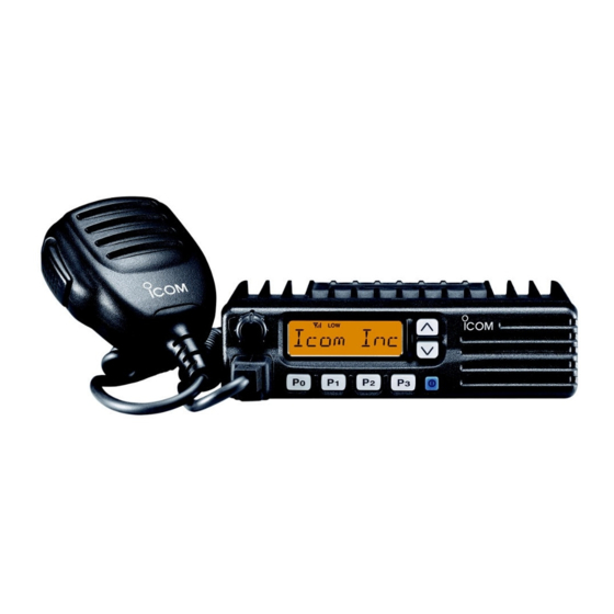
- Page 1 SERVICE MANUAL UHF TRANSCEIVER iF210 iF211 iF221...
- Page 2 This service manual describes the latest service information NEVER connect the transceiver to an AC outlet or to a DC for the IC-F210, F211 and F221 UHF MOBILE TRANSCEIV- power supply that uses more than 16 V. This will ruin the transceiver.
- Page 3 EXPLICIT DEFINITIONS FREQUENCY COVERAGE CHANNEL SPACING Low band 400-430 MHz Wide/Narrow-type 12.5 kHz/ 25.0 kHz Middle band 440-490 MHz Middle/Narrow-type 12.5 kHz/ 20.0 kHz TABLE OF CONTENTS SECTION 1 SPECIFICATIONS SECTION 2 INSIDE VIEW SECTION 3 DISASSEMBLY INSTRUCTIONS SECTION 4 CIRCUIT DESCRIPTION 4 - 1 RECEIVER CIRCUITS .
- Page 4 SECTION 1 SPECIFICATIONS [GEN], [USA] [EUR] Measurement method EIA-152-C/204D or TIA-603 ETS 300 086 Frequency coverage* 400.000–430.000 MHz or 440.000–490 MHz N/W: (12.5 kHz; Narrow/25 kHz; Wide): 8K50F3E/16K0F3E [EUR] Type of emission (12.5 kHz; Narrow/25 kHz; Wide): 8K50F3E/16K0F3E [USA], [GEN] N/M (12.5 kHz;...
- Page 5 SECTION 2 INSIDE VIEW Final FET module : RA30H4452M-21[25W-M] : RA30H4047M-21[25W-L] : RA45H4452M-21[45W-M] : RA45H4047M-21[45W-L] Antenna switch/ CPU 5V regurator* Low-pass filter circuit (IC10: AN78L05M) 8V regurator Mixer* (IC9: TA7808F) (Q3: 3SK299) 2nd IF filter* (FI2: ALFYM450F=K) VCO circuit D/A converter* (IC6: M62363FP-650C) AF amplifier (IC8: LA4425A)
- Page 6 SECTION 3 DISASSEMBLY INSTRUCTIONS • Opening case and removing the front unit Unscrew 8 screws H. Unscrew 4 screws A, and remove the bottom cover. Remove the filter case I. Disconnect the flat cable B from J2. Unscrew the screw J. Disconnect the cable C from J7.
-
Page 7: Receiver Circuits
SECTION 4 CIRCUIT DESCRIPTION 4-1 RECEIVER CIRCUITS 4-1-3 1ST MIXER AND 1ST IF CIRCUITS (MAIN UNIT) 4-1-1 ANTENNA SWITCHING CIRCUIT The 1st mixer circuit converts the received signals to a fixed (MAIN UNIT) frequency of the 1st IF signal with the PLL output frequency. The antenna switching circuit functions as a low-pass filter By changing the PLL frequency, only the desired frequency while receiving and as resonator circuit while transmitting. -
Page 8: Transmitter Circuits
4-1-5 AF AMPLIFIER CIRCUIT (MAIN UNIT) 4-2 TRANSMITTER CIRCUITS The AF amplifier circuit amplifies the demodulated AF sig- 4-2-1 MICROPHONE AMPLIFIER CIRCUIT nals to drive a speaker. (MAIN AND FRONT UNITS) The microphone amplifier circuit amplifies audio signals The AF signals from the FM IF IC (IC1, pin 9) are applied to within +6 dB/octave pre-emphasis characteristics from the the active filter circuit (IC16). -
Page 9: Pll Circuits
4-2-4 POWER AMPLIFIER CIRCUIT (MAIN UNIT) 4-3 PLL CIRCUITS The power amplifier circuit amplifies the driver signal to an 4-3-1 PLL CIRCUIT (MAIN UNIT) output power level. A PLL circuit provides stable oscillation of the transmit fre- quency and receive 1st LO frequency. The PLL output com- The RF signal from the drive amplifier (Q8) is passed pares the phase of the divided VCO frequency to the refer- through the low-pass filter circuit (L18, L43, C89, C90, C92,... - Page 10 4-4 POWER SUPPLY CIRCUITS 4-5 PORT ALLOCATIONS 4-4-1 VOLTAGE LINES (MAIN UNIT) 4-5-1 CPU (FRONT UNIT; IC1) Description Line Port Description number name The voltage from a DC power supply. TEMP Input port for the internal temperature. The same voltage as the HV line which is con- Input port for the low voltage detection trolled by the power switching circuit (Q23, Q24).
- Page 11 CPU-Continued 4-5-2 OUTPUT EXPANDER (MAIN UNIT; IC17) Port Description Port number name Description number name OPT3– I/O ports for the optional board control Outputs transmit/receive control signal. 44–46 OPT1 signals. High: While receiving. Input port for the clock sigal from the Outputs audio output control signal.
- Page 12 • At least 16 MB RAM and 10 MB of hard disk space I STARTING SOFTWARE ADJUSTMENT • 640×480 pixel display (800×600 pixel display recommend- q Connect IC-F210/F211/F221 and PC with *OPC-1122 CABLE w Turn the transceiver power ON. IBM is a registered trademark of International Bussiness e Boot up Windows, and click the program group ‘CS-F100...
- Page 13 I REQUIRED TEST EQUIPMENT EQUIPMENT GRADE AND RANGE EQUIPMENT GRADE AND RANGE Output voltage : 13.2 V DC Frequency range : 300–3000 Hz DC power supply Audio generator Current capacity : 15 A or more Measuring range : 1–500 mV Measuring range : 1–100 W Frequency range...
- Page 14 • SCREEN DISPLAY EXAMPLE CS-F100 ADJ Rev.1.0 File Option COM 1: OPEN Connect Reload (F5) Disp para [A / D] [D / A] : 178 : B2h : 19.96 V BPF T1 : 197 : 32h : 0.98 V TEMPS : 177 : B1h : 26.44 ’C T2/POW : 172 : 32h : 0.98 V LVIN...
-
Page 15: Pll Adjustment
5-2 PLL ADJUSTMENT MEASUREMENT ADJUSTMENT ADJUSTMENT ADJUSTMENT CONDITIONS VALUE UNIT LOCATION UNIT ADJUST PLL LOCK • Operating freq. : 400.000 MHz MAIN Connect a digital multi- 1.0 V MAIN C133 VOLTAGE 440.000 MHz meter or an oscillo- • Receiving scope to the check point, “LV”. -
Page 16: Software Adjustment
5-3 SOFTWARE ADJUSTMENT Select an operation using [↑] / [↓] keys, then set specified value using [←] / [→] keys on the connected computer keyboard. MEASUREMENT ADJUSTMENT ADJUSTMENT CONDITION VALUE UNIT LOCATION REFERENCE • Operating freq. : 430.000 MHz Rear Loosely couple a frequnecy 430.0000 MHz FREQUENCY... - Page 17 SOFTWARE ADJUSTMENT – continued Select an operation using [↑] / [↓] keys, then set specified value using [←] / [→] keys on the connected computer keyboard. MEASUREMENT ADJUSTMENT ADJUSTMENT CONDITION VALUE UNIT LOCATION • Operating freq. : 400.000 MHz MAIN Connect a SINAD meter with a Minimum distortion 4 Ω...
- Page 18 5-4 TRIMMER ADJUSTMENT • Make this adjustment if necessary (For example, when beep sound is too loud or too soft). • BE CAREFUL!: 5-tone calling beep sound becomes loud or soft when beep volume adjusts to loud or soft. MEASUREMENT ADJUSTMENT ADJUSTMENT ADJUSTMENT CONDITIONS...
-
Page 19: Front Unit
SECTION 6 PARTS LIST [FRONT UNIT] [FRONT UNIT] ORDER ORDER DESCRIPTION DESCRIPTION 1140011260 S.IC HD6433687A11FP (FX-2622A) 7410001130 S.ARRAY EXB28V102JX 1110005770 S.IC S-80942CNMC-G9C-T2 7030005160 S.RESISTOR ERJ2GEJ 105 X (1 MΩ) 1140008650 S.IC HN58X2464TI 7030005050 S.RESISTOR ERJ2GEJ 103 X (10 kΩ) 1110005340 S.IC NJM12902V-TE1 7310002740 S.TRIMMER RV-150 (RH03A3A14X0FC) 103... -
Page 20: Main Unit
[FRONT UNIT] [MAIN UNIT] ORDER ORDER DESCRIPTION DESCRIPTION 4030017460 S.CERAMIC ECJ0EB1E102K 1550000020 S.FET 2SJ377 (TE16R) 4030016930 S.CERAMIC ECJ0EB1A104K 1590000430 S.TRANSISTOR DTC144EUA T106 4030016930 S.CERAMIC ECJ0EB1A104K 1540000550 S.TRANSISTOR 2SD1664 T100Q 4030017460 S.CERAMIC ECJ0EB1E102K 1510000920 S.TRANSISTOR 2SA1577 T106 Q 4030017420 S.CERAMIC ECJ0EC1H470J 1510000920 S.TRANSISTOR 2SA1577 T106 Q 4030017420 S.CERAMIC ECJ0EC1H470J... - Page 21 [MAIN UNIT] [MAIN UNIT] ORDER ORDER DESCRIPTION DESCRIPTION 6200007230 S.COIL LQW2BHN15NJ01L (LQN21A 15NJ04) 7030003490 S.RESISTOR ERJ3GEYJ 272 V (2.7 kΩ) 7030003520 S.RESISTOR ERJ3GEYJ 472 V (4.7 kΩ) 6200007680 S.COIL LQW2BHN12NJ01L (LQN21A 12NJ04) 7030003680 S.RESISTOR ERJ3GEYJ 104 V (100 kΩ) ERJ3GEYJ 470 V (47 Ω) 7030003280 S.RESISTOR 6200004660 S.COIL MLF1608A 1R8K-T...
- Page 22 [MAIN UNIT] [MAIN UNIT] ORDER ORDER DESCRIPTION DESCRIPTION R120 7030003560 S.RESISTOR ERJ3GEYJ 103 V (10 kΩ) R237 7030003780 S.RESISTOR ERJ3GEYJ 684 V (680 kΩ) R121 7030003520 S.RESISTOR ERJ3GEYJ 472 V (4.7 kΩ) R238 7030003680 S.RESISTOR ERJ3GEYJ 104 V (100 kΩ) R122 7030003460 S.RESISTOR ERJ3GEYJ 152 V (1.5 kΩ)
- Page 23 [MAIN UNIT] [MAIN UNIT] ORDER ORDER DESCRIPTION DESCRIPTION 4030011040 S.CERAMIC GRM31M4C2H2R0CY21L (GRM42-6 CK) 4030006990 S.CERAMIC C1608 CH 1H 080D-T 4030011770 S.CERAMIC C1608 CH 1H 060B-T 4030011050 S.CERAMIC GRM31M3C2H3R0CY21L (GRM42-6 CJ) 4030011030 S.CERAMIC GRM31M4C2H1R5CY21L (GRM42-6 CK) 4030007090 S.CERAMIC C1608 CH 1H 470J-T 4030011040 S.CERAMIC GRM31M4C2H2R0CY21L (GRM42-6 CK) 4030006860 S.CERAMIC...
- Page 24 [MAIN UNIT] [MAIN UNIT] ORDER ORDER DESCRIPTION DESCRIPTION C156 4030007090 S.CERAMIC C1608 CH 1H 470J-T C292 4030017420 S.CERAMIC ECJ0EC1H470J C157 4030007130 S.CERAMIC C1608 CH 1H 101J-T C293 4030017460 S.CERAMIC ECJ0EB1E102K C158 4030007130 S.CERAMIC C1608 CH 1H 101J-T C294 4030017460 S.CERAMIC ECJ0EB1E102K C159 4030011600 S.CERAMIC...
- Page 25 [MAIN UNIT] ORDER DESCRIPTION C388 4030007160 S.CERAMIC C1608 CH 1H 181J-T C389 4030011770 S.CERAMIC C1608 CH 1H 060B-T C390 4030017460 S.CERAMIC ECJ0EB1E102K C391 4030017420 S.CERAMIC ECJ0EC1H470J C392 4030006860 S.CERAMIC C1608 JB 1H 102K-T C393 4030009560 S.CERAMIC C1608 CH 1H R75B-T 4030009910 S.CERAMIC C1608 CH 1H 040B-T C394...
- Page 26 SECTION 7 MECHANICAL PARTS AND DISASSEMBLY [CHASSIS PARTS] [ACCESSORIES] REF. ORDER REF. ORDER DESCRIPTION QTY. DESCRIPTION QTY. 6510004880 Connector MR-DS-E 01 800005780 Microphone HM-100N 8010019060 2601 chassis [25W] 8900010990 Cable OPC-1132 [45W] 8010019130 2601 long chassis [45W] 8900011780 Cable OPC-1194 [25W] 8110007820 2601 cover...
- Page 27 MP10 (C) MP15 (C) J1 (C) MP10 (M) W2 (M) MP1 (C) MP13 (C) J4 (M) MP1 (M) MP11 (M) MP8 (M) MAIN UNIT MP2 (M) MP7 (M) MP13 (C) MP11 (C) MP2 (F) R14 (F) MP4 (M) MP3 (F) MP5 (M) MP9 (C) J1 (F)
- Page 28 SECTION 8 SEMI-CONDUCTOR INFORMATION • TRANSSISTORS AND FET’S • DIODES 2SA1577 T106 Q 2SC3356 T1B R25 2SC4116 BL 2SC4213 B 2SC4215 O 1SV307 DA221 TL DAN222TL DAP222 DSA3A1 (Symbol: HQ) (Symbol: R25) (Symbol: LL) (Symbol: AB) (Symbol: QO) (Symbol: TX) (Symbol: K) (Symbol: N) (Symbol: P)
- Page 29 SECTION 9 BOARD LAYOUTS 9-1 FRONT UNIT • TOP VIEW Microphone 9 - 1...
- Page 30 • BOTTOM VIEW (FRONT UNIT) to MAIN unit J2 9 - 2...
- Page 31 9-2 MAIN UNIT • TOP VIEW CHASSIS to DC cable speaker HORN DISC to Optional cable OPC-617 to Optional unit to FRONT unit J2 9 - 3...
- Page 32 • BOTTOM VIEW (MAIN UNIT) 9 - 4...
- Page 33 SECTION 10 BLOCK DIAGRAM 400-430 MHz Q15 XP1214 440-490 MHz RX VCO 2SC4116 Q16 DTC144EU 2SK880 2SC4226 D16 HVC350B CR-741 LVIN RIPPLE BUFF RA30H4452M-21[25W-M] RA30H4047M-21[25W-L] D2 UM9401F [25W] RA45H4452M-21[45W-M] D14 1SV307 D3 XB15A407 [45W] D1, D11 RA45H4047M-21[45W-L] MB15A02PFV-1 D15 MA77 D5 UM9401F MA728 HVC362...
- Page 34 SECTION 11 VOLTAGE DIAGRAMS 11-1 FRONT UNIT DS11 FRONT UNIT L2-0607TAY 5.0V R51 100k MA2S111 C79 0.1 COM3 SEG22 COM3 COM4 SEG21 COM4 SEG20 S-80942CNMC-G9C 5.0V TEMP P86/AN6 P70/SCK3_2 SEG19 BATV VLCD P87/AN7 SEG18 OPT2 VLCD1 AVCC P22/TXD SEG17 LC75834W OPT1 VLCD2 C35 0.1...
- Page 35 11-2 MAIN UNIT NOTE MAIN UNIT (1) : Middle band/ Low band 5.0V R110 2SC4116 2SK880 120k R220 C161 CR-741 7.0V 100k 100p 3.3k 3.3k R266 OV12 2SC4215 C200 C126 OV12 R267 OV12 DAST R268 DAST R210 C113 CIRQ CIRQ 100K 2SC4226 C163...
- Page 36 MAIN UNIT (2) NOTE : Middle band/ Low band : 25W/ 45W MEASUREMENT CONDITIONS VOLTMETER Amplitude(Oscilloscope) : 100 MHz Frequency : 465 MHz Transmission : 25 W 6.8V RA30H4452M-21[25W-M] RA30H4047M-21[25W-L] RA45H4452M-21[45W-M] RA45H4047M-21[45W-L] 3p[25W-L] TX: 6.3V 1.5p[45W-M] RX: 0V 6.4V 2p[Other] XB15A407[45W] AS080340-15N 1 2 3 4...
- Page 38 S-13906HZ-C1U-q 1-1-32, Kamiminami, Hirano-ku, Osaka 547-0003, Japan © 2003 Icom Inc.