Table of Contents
Advertisement
Quick Links
Advertisement
Table of Contents

Related Manuals for Icom IC F110S


Summary of Contents for Icom IC F110S
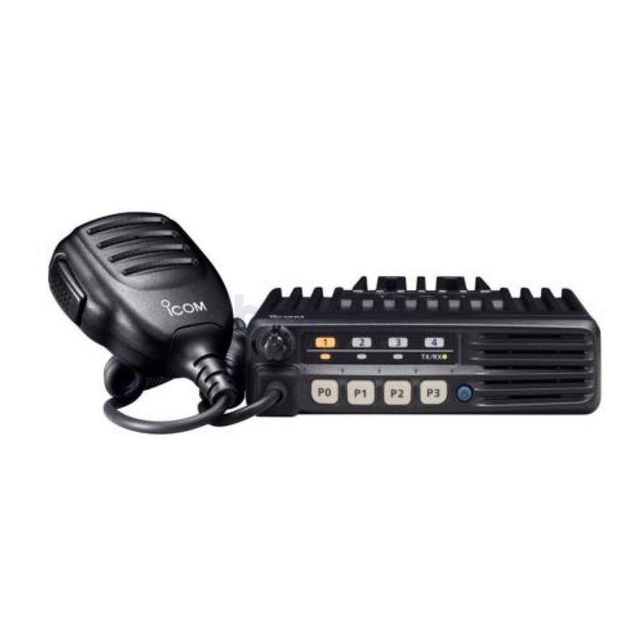
- Page 1 SERVICE MANUAL VHF TRANSCEIVER iF110S iF111S iF121S...
- Page 2 INTRODUCTION This service manual describes the latest service information for the IC-F110S, IC-F111S and IC-F121S VHF MOBILE TRANSCEIVER at the time of publication. MODEL VERSION Europe IC-F110S General IC-F111S General IC-F121S U.S.A. To upgrade quality, any electrical or mechanical parts and internal circuits are subject to change without notice or obligation.
- Page 3 FREQUENCY COVERAGE 136 – 174 MHz SECTION 1 SPECIFICATIONS SECTION 2 INSIDE VIEW SECTION 3 DISASSEMBLY INSTRUCTIONS SECTION 4 CIRCUIT DESCRIPTION 4 - 1 RECEIVER CIRCUITS ............4 - 1 4 - 2 TRANSMITTER CIRCUITS .
- Page 4 SECTION 1 SPECIFICATIONS Measurement method Frequency coverage Type of emission Number of conventional channels Antenna impedance Power supply voltage (negative ground) Current drain (approx.) Usable temperature range Dimensions (proj. not included) Weight RF output power Modulation system Maximum permissible deviation Frequency error Spurious emissions Adjacent channel power...
- Page 5 SECTION 2 INSIDE VIEW Antenna switch/ Low-pass filter circuit Mixer* (Q3: 3SK299) 2nd IF filter* (FI2: ALFYM450F=K) D/A converter* (IC6: M62363FP-650C) IF IC (IC1: TA31136FN) 1st IF filter (FI1: FL-335) * Located under side of the point. 2 - 1 Final FET module IC3: RA30H1317 [25W] S-AV32...
- Page 6 SECTION 3 DISASSEMBLY INSTRUCTIONS • Opening case and remove the front panel ➀ Unscrew 4 screws A, and remove the bottom cover. ➁ Disconnect the flat cable B from J2. ➂ Disconnect the cable C from J7. ➃ Unscrew 2 screws D , and remove the front unit in the direction of the arrow.
-
Page 7: Receiver Circuits
SECTION 4 CIRCUIT DESCRIPTION 4-1 RECEIVER CIRCUITS 4-1-1 ANTENNA SWITCHING CIRCUIT (MAIN UNIT) The antenna switching circuit functions as a low-pass filter while receiving and as resonator circuit while transmitting. This circuit does not allow transmit signals to enter the receiver circuits. -
Page 8: Transmitter Circuits
4-1-5 AF AMPLIFIER CIRCUIT (MAIN UNIT) The AF amplifier circuit amplifies the demodulated AF sig- nals to drive a speaker. The AF signals from the FM IF IC (IC1, pin 9) are applied to the active filter circuit (IC16). The active filter circuit (high- pass filter) removes CTCSS or DTCS signals. -
Page 9: Pll Circuits
4-2-4 POWER AMPLIFIER CIRCUIT (MAIN UNIT) The power amplifier circuit amplifies the driver signal to an output power level. The RF signal from the drive amplifier (Q8) is passed through the low-pass filter circuit (L18, C90, C89) and applied to the power module (IC3) to obtain 25 W or 50 W of RF power. -
Page 10: Power Supply Circuits
4-4 POWER SUPPLY CIRCUITS 4-4-1 VOLTAGE LINES (MAIN UNIT) Description Line The voltage from a DC power supply. The same voltage as the HV line which is con- trolled by the power switching circuit (Q23, Q24). When the [POWER] switch is pushed, the CPU outputs the “PWON”... - Page 11 CPU-Continued Port Description number name Outputs control signal for the power PWON switching circuit (MAIN unit; Q24, Q23). Outputs IF bandwidth control signal. Low : While IF bandwidth is narrow. Outputs control signal for the AF mute circuit (MAIN unit; Q35, Q36, D29). AFON High : While AF amplifier (MAIN unit;...
- Page 12 SECTION 5 ADJUSTMENT PROCEDURES 5-1 PREPARATION When you adjust the contents on pages 5-5 and 5-6, SOFT- WARE ADJUSTMENT, the optional CS-F100S ADJ (Rev. 1.0 or later), *OPC-1122 MENT SOFTWARE (modified OPC-1122 ; see illustration below) CLONING CABLE are required. I SYSTEM REQUIREMENTS •...
- Page 13 I REQUIRED TEST EQUIPMENT EQUIPMENT GRADE AND RANGE Output voltage DC power supply Current capacity Measuring range RF power meter Frequency range (terminated type) Impedance Frequency range Frequency counter Frequency accuracy : ±1 ppm or better Sensitivity Frequency range FM deviation meter Measuring range Digital maltimeter Input impedance...
- Page 14 • Screen display exampe CS-F100S ADJ Rev.1.0 File Option COM 1: OPEN [A / D] : 178 : B2h : 19.96 V TEMPS : 177 : B1h : 26.44 'C LVIN : 176 : B0h : 23 : 17h : CH No.
- Page 15 5-2 PLL ADJUSTMENT ADJUSTMENT ADJUSTMENT CONDITIONS PLL LOCK • Operating freq. : 174.000 MHz VOLTAGE • Receiving • Output power • Transmitting • Operating freq. : 136.000 MHz • Receiving • Output power • Transmitting PLL lock voltage check point MEASUREMENT UNIT LOCATION...
- Page 16 5-3 SOFTWARE ADJUSTMENT Select an operation using [↑] / [↓] keys, then set specified value using [←] / [→] keys on the connected computer keyboard. ADJUSTMENT ADJUSTMENT CONDITION REFERENCE • Operating freq. : 174.000 MHz FREQUENCY • Output power : Low1 •...
- Page 17 SOFTWARE ADJUSTMENT – continued Select an operation using [↑] / [↓] keys, then set specified value using [←] / [→] keys on the connected computer keyboard. ADJUSTMENT ADJUSTMENT CONDITION • Operating freq. : 136.000 MHz SENSITIVITY • IF bandwidth [BPF T1], •...
- Page 18 5-4 TRIMMER ADJUSTMENT • Make this adjustment if necessary (For example, when beep sound is too loud or too soft). • BE CAREFUL!: 5-tone calling beep sound becomes loud or soft when beep volume adjusts to loud or soft. ADJUSTMENT ADJUSTMENT CONDITIONS BEEP 1 •...
- Page 19 SECTION 6 PARTS LIST [FRONT UNIT] ORDER DESCRIPTION 1140010890 S.IC HD6433687A05FP 1110005770 S.IC S-80942CNMC-G9C-T2 1130010390 S.IC HN58X2416TI 1130009670 S.IC BU2092FV-E2 1110005340 S.IC NJM12902V-TE1 1530002060 S.TRANSISTOR 2SC4081 T106 R 1590001050 S.TRANSISTOR DTC114TUA T106 1590000430 S.TRANSISTOR DTC144EUA T106 1790000950 S.ZENER MA8056-M (TX) 1790000950 S.ZENER MA8056-M (TX) 1790000950 S.ZENER...
-
Page 20: Main Unit
[FRONT UNIT] ORDER DESCRIPTION 6510022470 S.CONNECTOR 40FLT-SM1-TB 5040002670 S.LED CL-165HR/YG 5040002310 S.LED SML-311YTT86 5040002310 S.LED SML-311YTT86 5040002310 S.LED SML-311YTT86 5040002310 S.LED SML-311YTT86 5040002310 S.LED SML-311YTT86 5040002310 S.LED SML-311YTT86 5040002310 S.LED SML-311YTT86 5040002310 S.LED SML-311YTT86 DS10 5040002310 S.LED SML-311YTT86 2510001220 SPEAKER C052SB500-13 8900010500 CABLE OPC-1046... - Page 21 [MAIN UNIT] ORDER DESCRIPTION 7030003560 S.RESISTOR ERJ3GEYJ 103 V (10 kΩ) 7030003610 S.RESISTOR ERJ3GEYJ 273 V (27 kΩ) 7030003610 S.RESISTOR ERJ3GEYJ 273 V (27 kΩ) 7030003620 S.RESISTOR ERJ3GEYJ 333 V (33 kΩ) ERJ3GEYJ 271 V (270 Ω) 7030003370 S.RESISTOR ERJ12YJ101U (100 Ω) 7030006070 S.RESISTOR ERJ3GEYJ 103 V (10 kΩ) B only 7030003560 S.RESISTOR...
- Page 22 [MAIN UNIT] ORDER DESCRIPTION ERJ3GEYJ 471 V (470 Ω) R215 7030003400 S.RESISTOR R216 7030003470 S.RESISTOR ERJ3GEYJ 182 V (1.8 kΩ) 7030003480 S.RESISTOR ERJ3GEYJ 222 V (2.2 kΩ) R217 7030003600 S.RESISTOR ERJ3GEYJ 223 V (22 kΩ) R218 7030003600 S.RESISTOR ERJ3GEYJ 223 V (22 kΩ) R219 7030003680 S.RESISTOR ERJ3GEYJ 104 V (100 kΩ)
- Page 23 [MAIN UNIT] ORDER DESCRIPTION 4030007030 S.CERAMIC C1608 CH 1H 150J-T 4030007020 S.CERAMIC C1608 CH 1H 120J-T 4030007090 S.CERAMIC C1608 CH 1H 470J-T 4030006860 S.CERAMIC C1608 JB 1H 102K-T 4030006860 S.CERAMIC C1608 JB 1H 102K-T 4030007090 S.CERAMIC C1608 CH 1H 470J-T 4030006860 S.CERAMIC C1608 JB 1H 102K-T C100...
- Page 24 [MAIN UNIT] ORDER DESCRIPTION C305 4030007100 S.CERAMIC C1608 CH 1H 560J-T C306 4030009910 S.CERAMIC C1608 CH 1H 040B-T C307 4030006980 S.CERAMIC C1608 CH 1H 070D-T C308 4030009530 S.CERAMIC C1608 CH 1H 030B-T C309 4030006900 S.CERAMIC C1608 JB 1H 103K-T C310 4030006860 S.CERAMIC C1608 JB 1H 102K-T C311...
- Page 25 SECTION 7 MECHANICAL PARTS [CHASSIS PARTS] REF. ORDER DESCRIPTION 6510004880 Connector MR-DS-E 01 8010019060 2601 chassis 8010019130 2601 long chassis 8110007820 2601 cover 8810008660 Screw PH BT M3 8810008660 Screw PH BT M3 8810008660 Screw PH BT M3 8810008660 Screw PH BT M3 8810009990 Screw PH BT M3 8810009990...
- Page 26 MP8 (C) R14 (F) J1 (F) MP10 (F) MP1 (F) MP4 (F) MP5 (F) MP3 (F) 7 - 2 J1 (C) MP1 (C) MAIN UNIT MP7 (M) MP6 (C) MP5 (C) W1 (F) MP7 (F) MP8 (F) FRONT UNIT MP2 (F) SP1 (F) MP7 (C) MP9 (F)
- Page 27 SECTION 8 SEMI-CONDUCTOR INFORMATION • TRANSISTORS AND FET’S 2SA1577 T106 Q 2SC3356 T1B R25 2SC4081 T106 R (Symbol: HQ) (Symbol: R25) (Symbol: BR) 2SC4226 T1 R25 2SC5107 O 2SD1664 T100Q (Symbol: R25) (Symbol: MFO) (Symbol: DAQ) 2SK880 Y 2SK1829 3SK293 (Symbol: XY) (Symbol: K1) (Symbol: UF)
- Page 28 SECTION 9 BOARD LAYOUTS 9-1 FRONT UNIT • TOP VIEW Microphone 9 - 1...
- Page 29 • BOTTOM VIEW (FRONT UNIT) to MAIN unit J2 9 - 2...
- Page 30 9-2 MAIN UNIT • TOP VIEW CHASSIS to Optional unit 9 - 3 to FRONT unit J2 to DC cable speaker HORN DISC to Optional cable OPC-617...
- Page 31 • BOTTOM VIEW (MAIN UNIT) 9 - 4...
- Page 32 SECTION 10 BLOCK DIAGRAM RX VCO 2SC4116 2SK880 2SC4226 D33, D34 HVC376B CR-740 LVIN RIPPLE BUFF MB15A02PFV-1 HVC362 2SC4215 15.3 MHz LOOP 1SV239 TX VCO 2SC4116 2SC4226 D16, D31 HVC376B 45.9 MHz IF IC IC1 TA31136FN DTC144EU CERAMIC RSSI SQIN CDBC450CX24 ALFYM450F=K 450 kHz...
- Page 33 SECTION 11 VOLTAGE DIAGRAMS 11-1 FRONT UNIT FRONT UNIT CL-165HR/YG R1 1.8k TLED R2 390 RLED BU2092FV DATA 5 CH1 1.5k 1.5k DS10 Dim ON: 2.6V OFF: 7.2V DS2-10 SML-311YT DTC114TU 2SC4081 MA8056 100k TX: 0V RX: 4.9V 7.9V MICE Jack 100k R51 100k...
- Page 34 11-2 MAIN UNIT MAIN UNIT (1) R110 R220 R266 R221 OV12 R267 OV12 DAST R268 DAST CIRQ CIRQ C163 R222 OPT3 OPT3 OPT2 OPT2 DISC DISC OPT1 OPT1 Optional SIGO SIGO unit BEEPO BEEPO UNLK BUSY BUSY AFONO AFONO PLST R271 100k CP24...
- Page 35 MAIN UNIT (2) 6.1V 6.4V TX: 3.1V C102 C100 RX: 0V 2SC3356 MA77 2SC5107 5.0V 2SC5107 TX: 2.3V RX: 2.1V TX: 0V RX: 2.9V 2SC5107 MA2S111 TX: 0V RX: 6.4V Lo level 1~3dBm TX: 0V RX: 7.3V C343 0.01 MAIN UNIT 3SK299 1.5p...
- Page 37 S-13906HZ-C1VS-e 1-1-32, Kamiminami, Hirano-ku, Osaka 547-0003, Japan © 2003 Icom Inc.
- Page 38 SERVICE MANUAL UHF TRANSCEIVER iF210S iF211S iF221S...
- Page 39 INTRODUCTION This service manual describes the latest service information for the IC-F210S, IC-F211S and IC-F221S UHF MOBILE TRANSCEIVER at the time of publication. MODEL VERSION Europe IC-F210S General IC-F211S General IC-F221S U.S.A. To upgrade quality, any electrical or mechanical parts and internal circuits are subject to change without notice or obligation.
- Page 40 FREQUENCY COVERAGE Low Band 400-430 MHz High Band 440-490 MHz SECTION 1 SPECIFICATIONS SECTION 2 INSIDE VIEW SECTION 3 DISASSEMBLY INSTRUCTIONS SECTION 4 CIRCUIT DESCRIPTION 4 - 1 RECEIVER CIRCUITS ............4 - 1 4 - 2 TRANSMITTER CIRCUITS .
- Page 41 SECTION 1 SPECIFICATIONS Measurement method Frequency coverage Type of emission Number of conventional channels Power supply voltage (negative ground) Current drain (approx.) Antenna impedance Usable temperature range Dimensions (proj. not included) Weight RF output power Modulation system Maximum permissible deviation Frequency error Spurious emissions Adjacent channel power...
- Page 42 SECTION 2 INSIDE VIEW Antenna switch/ Low-pass filter circuit Mixer* (Q3: 3SK299) 2nd IF filter* (FI2: ALFYM450F=K) D/A converter* (IC6: M62363FP-650C) IF IC (IC1: TA31136FN) 1st IF filter FI1: FL-335 [EUR] FL-313 [USA],[GEN] * Located under side of the point. 2 - 1 Final FET module : RA30H4452M-21 [25W-H]...
- Page 43 SECTION 3 DISASSEMBLY INSTRUCTIONS • Opening case and removing the front unit Unscrew 4 screws A, and remove the bottom cover. Disconnect the flat cable B from J2. Disconnect the cable C from J7. Unscrew 2 screws D , and remove the front unit in the direction of the arrow.
- Page 44 SECTION 4 CIRCUIT DESCRIPTION 4-1 RECEIVER CIRCUITS 4-1-1 ANTENNA SWITCHING CIRCUIT (MAIN UNIT) The antenna switching circuit functions as a low-pass filter while receiving and as resonator circuit while transmitting. This circuit does not allow transmit signals to enter the receiver circuits.
- Page 45 4-1-5 AF AMPLIFIER CIRCUIT (MAIN UNIT) The AF amplifier circuit amplifies the demodulated AF sig- nals to drive a speaker. The AF signals from the FM IF IC (IC1, pin 9) are applied to the active filter circuit (IC16). The active filter circuit (high- pass filter) removes CTCSS or DTCS signals.
- Page 46 4-2-4 POWER AMPLIFIER CIRCUIT (MAIN UNIT) The power amplifier circuit amplifies the driver signal to an output power level. The RF signal from the drive amplifier (Q8) is passed through the low-pass filter circuit (L18, C90, C89) and applied to the power module (IC3) to obtain 25 W or 45 W of RF power.
- Page 47 4-4 POWER SUPPLY CIRCUITS 4-4-1 VOLTAGE LINES (MAIN UNIT) Description Line The voltage from a DC power supply. The same voltage as the HV line which is con- trolled by the power switching circuit (Q23, Q24). When the [POWER] switch is pushed, the CPU outputs the “PWON”...
- Page 48 CPU-Continued Port Description number name Outputs control signal for the power PWON switching circuit (MAIN unit; Q23, Q24). Outputs IF bandwidth control signal. Low : While IF bandwidth is narrow. Outputs control signal for the AF mute circuit (MAIN unit; Q35, Q36, D29). AFON High : While AF amplifier (MAIN unit;...
- Page 49 SECTION 5 ADJUSTMENT PROCEDURES 5-1 PREPARATION When you adjust the contents on pages 5-5 and 5-6, SOFT- WARE ADJUSTMENT, the optional CS-F100S ADJ (Rev. 1.0 or later), *OPC-1122 MENT SOFTWARE (modified OPC-1122 CLONING CABLE are required. I SYSTEM REQUIREMENTS • IBM PC compatible computer with an RS -232C serial port (38400 bps or faster).
- Page 50 I REQUIRED TEST EQUIPMENT EQUIPMENT GRADE AND RANGE Output voltage DC power supply Current capacity Measuring range RF power meter Frequency range (terminated type) Impedance Frequency range Frequency counter Frequency accuracy : ±1 ppm or better Sensitivity Frequency range FM deviation meter Measuring range Digtal multimeter Input impedance...
- Page 51 • Screen display exampe CS-F100S ADJ Rev.1.0 File Option COM 1: OPEN [A / D] : 178 : B2h : 19.96 V TEMPS : 177 : B1h : 26.44 'C LVIN : 176 : B0h : 23 : 17h : CH No.
- Page 52 5-2 PLL ADJUSTMENT ADJUSTMENT ADJUSTMENT CONDITIONS PLL LOCK • Operating freq. : 400.000 MHz [L] VOLTAGE • Receiving • Output power • Transmitting • Operating freq. : 430.000 MHz [L] • Receiving • Output power • Transmitting PLL lock voltage check point MEASUREMENT UNIT...
- Page 53 5-3 SOFTWARE ADJUSTMENT Select an operation using [↑] / [↓] keys, then set specified value using [←] / [→] keys on the connected computer keyboard. ADJUSTMENT ADJUSTMENT CONDITION REFERENCE • Operating freq. : 490.000 MHz FREQUENCY [TXF] • Output power : Low1 •...
- Page 54 SOFTWARE ADJUSTMENT – continued Select an operation using [↑] / [↓] keys, then set specified value using [←] / [→] keys on the connected computer keyboard. ADJUSTMENT ADJUSTMENT CONDITION • Operating freq. : 400.000 MHz [L] SENSITIVITY [BPF T1], • IF bandwidth [BPF T2] •...
- Page 55 5-4 TRIMMER ADJUSTMENT • Make this adjustment if necessary (For example, when beep sound is too loud or too soft). • BE CAREFUL!: 5-tone calling beep sound becomes loud or soft when beep volume adjusts to loud or soft. ADJUSTMENT ADJUSTMENT CONDITIONS BEEP 1 •...
- Page 56 SECTION 6 PARTS LIST [FRONT UNIT] ORDER DESCRIPTION 1140010890 S.IC HD6433687A05FP 1110005770 S.IC S-80942CNMC-G9C-T2 1130010390 S.IC HN58X2416TI 1130009670 S.IC BU2092FV-E2 1110005340 S.IC NJM12902V-TE1 1530002060 S.TRANSISTOR 2SC4081 T106 R 1590001050 S.TRANSISTOR DTC114TUA T106 1590000430 S.TRANSISTOR DTC144EUA T106 1790000950 S.ZENER MA8056-M (TX) 1790000950 S.ZENER MA8056-M (TX) 1790000950 S.ZENER...
- Page 57 [FRONT UNIT] ORDER DESCRIPTION 6510022470 S.CONNECTOR 40FLT-SM1-TB 5040002670 S.LED CL-165HR/YG 5040002310 S.LED SML-311YTT86 5040002310 S.LED SML-311YTT86 5040002310 S.LED SML-311YTT86 5040002310 S.LED SML-311YTT86 5040002310 S.LED SML-311YTT86 5040002310 S.LED SML-311YTT86 5040002310 S.LED SML-311YTT86 5040002310 S.LED SML-311YTT86 DS10 5040002310 S.LED SML-311YTT86 2510001220 SPEAKER C052SB500-13 8900010500 CABLE OPC-1046...
- Page 58 [MAIN UNIT] ORDER DESCRIPTION 6200005690 S.COIL ELJRE 18NG-F 6200002850 S.COIL NL 252018T-R82J 6200002840 S.COIL NL 252018T-R22J 6200006980 S.COIL ELJRE R10G-F 6200005690 S.COIL ELJRE 18NG-F 6200005710 S.COIL ELJRE 27NG-F 7030000620 S.RESISTOR MCR10EZHJ 100 kΩ MCR10EZHJ 47 Ω (470) 7030000220 S.RESISTOR MCR10EZHJ 47 Ω (470) 7030000220 S.RESISTOR ERJ3GEYJ 101 V (100 Ω) 7030003320 S.RESISTOR...
- Page 59 [MAIN UNIT] ORDER DESCRIPTION R195 7030003490 S.RESISTOR ERJ3GEYJ 272 V (2.7 kΩ) R196 7030003560 S.RESISTOR ERJ3GEYJ 103 V (10 kΩ) R197 7030003560 S.RESISTOR ERJ3GEYJ 103 V (10 kΩ) R198 7030003560 S.RESISTOR ERJ3GEYJ 103 V (10 kΩ) R199 7030003560 S.RESISTOR ERJ3GEYJ 103 V (10 kΩ) R200 7030003560 S.RESISTOR ERJ3GEYJ 103 V (10 kΩ)
- Page 60 [MAIN UNIT] ORDER DESCRIPTION 4030006860 S.CERAMIC C1608 JB 1H 102K-T 4030006860 S.CERAMIC C1608 JB 1H 102K-T 4030011810 S.CERAMIC C1608 JB 1A 224K-T 4030006880 S.CERAMIC C1608 JB 1H 472K-T 4030006860 S.CERAMIC C1608 JB 1H 102K-T 4030011040 S.CERAMIC GRM31M4C2H2R0CY21L 4030011050 S.CERAMIC GRM31M3C2H3R0CY21L 4030011040 S.CERAMIC GRM31M4C2H2R0CY21L 4030011050 S.CERAMIC...
- Page 61 [MAIN UNIT] ORDER DESCRIPTION C293 4030006860 S.CERAMIC C1608 JB 1H 102K-T C294 4030006860 S.CERAMIC C1608 JB 1H 102K-T C295 4510004630 S.ELECTROLYTIC ECEV1CA100SR C297 4030007010 S.CERAMIC C1608 CH 1H 100D-T C298 4030006980 S.CERAMIC C1608 CH 1H 070D-T C299 4030006980 S.CERAMIC C1608 CH 1H 070D-T C301 4030011340 S.CERAMIC C1608 CH 1H 471J-T...
- Page 62 SECTION 7 MECHANICAL PARTS [CHASSIS PARTS] REF. ORDER DESCRIPTION 6510004880 Connector MR-DS-E 01 8010019060 2601 chassis 8010019130 2601 long chassis 8110007820 2601 cover 8810008660 Screw PH BT M3 8810008660 Screw PH BT M3 8810008660 Screw PH BT M3 8810008660 Screw PH BT M3 8810009990 Screw PH BT M3 8810009990...
- Page 63 MP8 (C) R14 (F) J1 (F) MP10 (F) MP1 (F) MP4 (F) MP5 (F) MP3 (F) 7 - 2 J1 (C) MP1 (C) MAIN UNIT MP7 (M) MP6 (C) MP5 (C) MP8 (F) MP12 (C) MP7 (F) W1 (F) FRONT UNIT MP2 (F) SP1 (F) MP7 (C)
- Page 64 SECTION 8 SEMI-CONDUCTOR INFORMATION • TRANSISTORS AND FET’S 2SA1577 T106 Q 2SC3356 T1B R25 2SC4081 T106 R (Symbol: HQ) (Symbol: R25) (Symbol: BR) 2SC4226 T1 R25 2SC5107 O 2SD1664 T100Q (Symbol: R25) (Symbol: MFO) (Symbol: DAQ) 2SK880 Y 2SK1829 3SK293 (Symbol: XY) (Symbol: K1) (Symbol: UF)
- Page 65 SECTION 9 BOARD LAYOUTS 9-1 FRONT UNIT • TOP VIEW Microphone 9 - 1...
- Page 66 • BOTTOM VIEW (FRONT UNIT) to MAIN unit J2 9 - 2...
- Page 67 9-2 MAIN UNIT • TOP VIEW CHASSIS to Optional unit 9 - 3 to FRONT unit J2 to DC cable speaker HORN DISC to Optional cable OPC-617...
- Page 68 • BOTTOM VIEW (MAIN UNIT) 9 - 4...
- Page 69 SECTION 10 BLOCK DIAGRAM RX VCO 2SC4116 2SK880 2SC4226 D16 HVC350B CR-741 LVIN RIPPLE BUFF 2SC4215 MB15A02PFV-1 HVC362 15.3 MHz LOOP MA368 2SC4116 TX VCO 2SC4226 D17 HVC350B 45.9 MHz IF IC IC1 TA31136FN DTC144EU CERAMIC RSSI SQIN CDBC450CX24 ALFYM450F=K 450 kHz NJM12904V IC16...
- Page 70 SECTION 11 VOLTAGE DIAGRAMS 11-1 FRONT UNIT FRONT UNIT CL-165HR/YG R1 1.8k TLED R2 390 RLED BU2092FV DATA 5 CH1 1.5k 1.5k DS10 Dim ON: 2.6V OFF: 7.2V DS2-10 SML-311YT DTC114TU 2SC4081 MA8056 100k TX: 0V RX: 4.9V 7.9V MICE Jack 100k R51 100k...
- Page 71 11-2 MAIN UNIT MAIN UNIT (1) R110 R220 100k R266 OV12 R267 OV12 DAST R268 DAST CIRQ CIRQ C163 R222 OPT3 OPT3 OPT2 OPT2 DISC DISC OPT1 OPT1 Optional SIGO SIGO unit BEEPO BEEPO UNLK BUSY BUSY AFONO AFONO PLST R271 540mVrms (40mVrms at mic terminal)
- Page 72 MAIN UNIT (2) 6.8V TX: 6.5V RX: 0V 6.3V TX: 3.0V RX: 0V C102 C100 1SV307 2SC5107 6.0V 2SC5107 TX: 2.3V 2SC5107 RX: 2.2V TX: 0V RX: 3.0V 2SC5107 TX: 0V RX: 7.5V TX: 0V 5p/7p RX: 7.3V C343 0.001 MAIN UNIT 3SK299...
- Page 74 S-13906HZ-C1US-w 1-1-32, Kamiminami, Hirano-ku, Osaka 547-0003, Japan C 2002, 2003 Icom Inc.