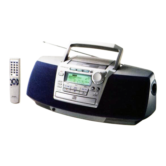
Aiwa CSD-EL33 Service Manual
Compact disc stereo cassette recorder
Hide thumbs
Also See for CSD-EL33:
- Service manual (30 pages) ,
- Operating instructions manual (16 pages)

Related Manuals for Aiwa CSD-EL33


Summary of Contents for Aiwa CSD-EL33
- Page 1 CSD-EL33 U HA SERVICE MANUAL COMPACT DISC STEREO BASIC TAPE MECHANISM : 2ZM-1 YR7NC CASSETTE RECORDER BASIC CD MECHANISM : 3ZG-3 E2NC S/M Code No. 09-995-330-1N1...
-
Page 2: Specifications
SPECIFICATIONS <General> <Tuner section> Speakers 100 mm cone type (2) (FM) Power output 2.5 W + 2.5 W (10% T.H.D./7Ω DC) Tuning range 87.5 MHz to 108.0 MHz 2 W + 2 W (DIN 1% Rated Power) Antenna Rod antenna Output Headphones (stereo minijack) Power requirements... -
Page 3: Protection Of Eyes From Laser Beam During Servicing
PROTECTION OF EYES FROM LASER BEAM DURING SERVICING This set employs laser. Therefore, be sure to follow carefully the CAUTION instructions below when servicing. Use of controls or adjustments or performance of procedures other than those specified herein may result in hazardous WARNING! radiation exposure. -
Page 4: Electrical Main Parts List
ELECTRICAL MAIN PARTS LIST REF. NO PART NO. KANRI DESCRIPTION REF. NO PART NO. KANRI DESCRIPTION C238 87-010-401-080 CAP, ELECT 1-50V C251 87-010-400-080 CAP, ELECT 0.47-50V C252 87-010-400-080 CAP, ELECT 0.47-50V 87-A20-459-010 C-IC,LC78622ED C255 87-010-546-080 CAP, ELECT 0.33-50V 8Z-CH1-622-010 IC,LC867132V-5G68 C256 87-010-546-080 CAP, ELECT 0.33-50V... - Page 5 REF. NO PART NO. KANRI DESCRIPTION REF. NO PART NO. KANRI DESCRIPTION C446 87-018-209-080 CAP, CER 0.1-50V FFC3 88-905-141-110 FF-CABLE, 5P 1.25 C447 87-018-209-080 CAP, CER 0.1-50V J201 87-009-216-010 JACK, DIA 3.5 C448 87-018-111-080 CAP, CERA-SOL SS 27P L301 87-003-102-080 COIL, 10UH C450 87-018-127-080...
- Page 6 REF. NO PART NO. KANRI DESCRIPTION REF. NO PART NO. KANRI DESCRIPTION S614 87-A90-095-080 SW,TACT EVQ11G04M 87-010-322-080 C-CAP,S 100P-50 CH S615 87-A90-095-080 SW,TACT EVQ11G04M 87-010-197-080 CAP, CHIP 0.01 DM S616 87-A90-095-080 SW,TACT EVQ11G04M 87-015-819-080 CAPACITOR,0.01 S617 87-A90-095-080 SW,TACT EVQ11G04M 87-010-196-080 CHIP CAPACITOR,0.1-25 S618 87-A90-095-080...
-
Page 7: Chip Resistor Part Code
CHIP RESISTOR PART CODE Chip Resistor Part Coding Figure Resistor Code Value of resistor Chip resistor Dimensions (mm) Wattage Type Tolerance Symbol Resistor Code Form 1/16W 1005 0.35 1/16W 1608 0.45 1/10W 2125 1.25 0.45 1/8W 3216 0.55 TRANSISTOR ILLUSTRATION S D G E C B E C B... -
Page 8: Ic Block Diagrams
IC BLOCK DIAGRAMS IC, M62439SP IC, BU4052BC... - Page 9 IC, TA7291S IC, LA6541D IC, LC72121M IC, BU2092 IC, TA2104AN IC, NJU7201L55...
- Page 10 SCHEMATIC DIAGRAM-1 (MAIN-AMP SECTION) <HA> <U> R561 1/4W <HA> Q501 2SA933S R507 R508 Q502 DTC124XS Q501, 502 D502 OPE LED 1N4148 DRIVER D501 1N4148 <U> J701 <U>: AC120V, 60Hz <HA>: AC110–120V /AC220–240V 50/60Hz <U> <U>: T3.15A 250V <HA>: T2.5A 250V S701 AC VOLTAGE 110V–120V...
- Page 11 WIRING-1 (MAIN, TUNER SECTION) D TUNER C.B ROD ANT. SPEAKER SPEAKER CN11 (AM BAR ANT.) CN12 To B FRONT C.B CNA601 A MAIN C.B Q524 Q525 R529 C527 Q523 C528 C930 Q331 Q332 R333 Q527 C340 C929 C338 C337 C382 D529 R339 R340...
-
Page 12: Fl Grid Assignment And Anode Connection
IC DESCRIPTION-1 IC, LC867132V-5L08 Pin No. Pin Name Description Pin No. Pin Name Description – – Not connected. O-MOT DECK mechanism motor control output. O-DATA Data for shift register 2092, PLL LC72121 and IC M62439. O-PL1 – Not connected. O-CLK Clock for shift register 2092 and PLL LC72121. - Page 13 SCHEMATIC DIAGRAM-2 (TUNER SECTION) 3.2(3.8) (3.8) (0.7) (0.9) (0.9) (2.7) (1.3) 4.8(4.6) 4.2(0) C30, C31 <U>: 0.022 <HA>: 0.015 0 (0.1) 0.4 1.2 1.2 0 5.4 0.8(0) 0(0.6) 0(3.6) Q071, Q072 IF GAIN CONTROL 2.2(0) FM IF AMP...
- Page 14 WIRING-2 (CD, TAPE SECTION) E LOADING MOTOR C.B G DECK C.B CON3 To B FRONT C.B CNA602 (REC B) (STOP) (CST) (REC A) (OPEN) (CLOSE) (LOADING MOTOR) FFC3 PIN1 To A MAIN C.B CN103 SFR1 (DECK MOTOR) F CD MOTOR C.B WHT1 SOL2 To A...
- Page 15 SCHEMATIC DIAGRAM-3 (MAIN-CD SECTION)
- Page 16 WIRING-3 (FRONT, POWER SECTION) S603 S602 S605 S604 S606 S607 CLEAR TUNING - PRESET TUNING + S616 S611 S617 B FRONT C.B REC/ REC MUTE Q SURROUND CD OPEN T-BASS STOP PAUSE PLAY/DIR S620 S603 S602 S605 S604 S606 S607 S611 S620 CN601...
- Page 17 SCHEMATIC DIAGRAM-4 (FRONT SECTION) LCD601 ZCH-2 (DISPLAY) D651 ~ D660 (DISPLAY BACK LIGHT) 1 2 3 4 5 6 7 8 9 10 11 12 13 14 15 16 17 18 19 20 21 22 23 24 25 26 27 28 29 30 31 32 33 S618 ~ 620 3-MODE EQUALIZER S608...
- Page 18 IC DESCRIPTION-2 IC, LC78622E Pin No. Pin Name Description Pin No. Pin Name Description DEFI Defect sense signal (DEF) input pin. (Connect to 0V when not used). XVDD — Crystal oscillator power supply pin. XOUT Test signal input pin with built-in pull-down resistor. Be sure to connect to 0V. Pin to which external 16.9344 MHz crystal oscillator is connected.
- Page 19 IC, LA9241ML Pin No. Pin Name Description Pin to which external pickup photo diode is connected. RF signal is created by adding FIN2 with the FIN1 pin signal. FE signal is created by subtracting from the FIN1 pin signal. FIN1 Pin to which external pickup photo diode is connected.
- Page 20 Pin No. Pin Name Description Pin from which TES signal is output to DSP. “High Frequency Level” is used to judge whether the main beam position is on top of bit or on top of mirror. SLOF Sled servo off control input pin. 39, 40 CV–, CV+ CLV error signal input pin from DSP.
-
Page 21: Electrical Adjustment
ELECTRICAL ADJUSTMENT <TUNER SECTION> <DECK SECTION> 1. AM VT Adjustment 6. Head Azimuth Adjustment D TUNER C.B (Top View) Settings: • Test point: TP1 (VT) Settings: • Test Tape: TTA-320 (TTA-113B, TTC-152) • Adjustment location: L4 • Test point: J201 (PHONES Jack) Method: Set to AM 1710 kHz and adjust L4 so that the test point •... -
Page 22: Mechanical Exploded View
MECHANICAL EXPLODED VIEW 1/1 WASHER LID,BATT PIPE,DUST L BATT C.B POWER CHASS,CASS PIPE,DUCT R CHAS,TU TUNE C.B CASS, MECHA LED C.B CD,MECHA MAIN C.B CHAS,CENTER FROPNT C.B... -
Page 23: Mechanical Main Parts List
MECHANICAL MAIN PARTS LIST REF. NO PART NO. KANRI DESCRIPTION REF. NO PART NO. KANRI DESCRIPTION 1 86-CT9-039-010 BADGE,AIWA 30N 34 87-A60-178-010 JACK,AC E W/SW<HA> 2 88-CD5-027-010 PANEL FR EX 35 88-CD5-207-010 SPR-C,BATT - 3 8Z-CH2-020-010 KNOB,RTRY VOL 36 88-CD5-041-010... -
Page 24: Cd Mechanism Exploded View
CD MECHANISM EXPLODED VIEW 1 / 2 3ZG3 LOADING MOTOR C.B... - Page 25 CD MECHANISM EXPLODED VIEW 2 / 2 CD MECHANISM PARTS LIST 1 / 2 If can’t understand for Description please kindly refer to “ REFERENCE NAME LIST ”. REF. NO. PART NO. KANRI DESCRIPTION REF. NO. PART NO. KANRI DESCRIPTION 1 83-ZG3-224-119 1B HLDR,M2 16 83-ZG3-211-01K 0E PLATE,DISC 2 83-ZG3-228-21K 1C CHAS,L6...
-
Page 26: Tape Mechanism Exploded View
TAPE MECHANISM EXPLODED VIEW 1/1 DECK C.B SOL2 RELAY C.B HLDR WIRE 3... -
Page 27: Tape Mechanism Parts List
TAPE MECHANISM PARTS LIST 1 / 1 If can’t understand for Description please kindly refer to “ REFERENCE NAME LIST ”. REF. NO. PART NO. KANRI DESCRIPTION REF. NO. PART NO. KANRI DESCRIPTION 1 82-ZM1-327-210 1D CHAS ASSY,RN 33 82-ZM1-227-210 0E LVR,TRIG 2 82-ZM1-258-010 0E SPR-T,PINCH L 34 82-ZM1-224-410 0E LVR,FR 3 82-ZM1-341-010 1A LVR ASSY,PINCH L 2... -
Page 28: Spring Application Position
SPRING APPLICATION POSITION... - Page 29 2–11, IKENOHATA 1–CHOME, TAITO-KU, TOKYO 110-8710, JAPAN TEL:03 (3827) 3111 Printed in Singapore 920074...