Table of Contents
Advertisement
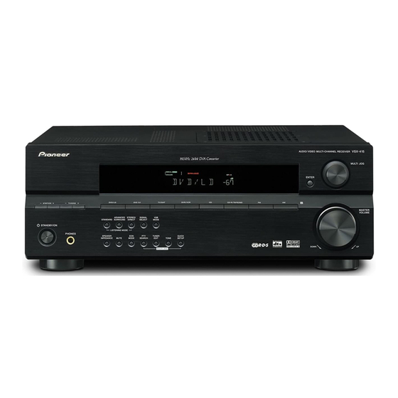
AUDIO/VIDEO MULTI-CHANNEL RECEIVER
VSX-417-K
VSX-417-S
THIS MANUAL IS APPLICABLE TO THE FOLLOWING MODEL(S) AND TYPE(S).
Model
Type
VSX-417-K
MYXJ5
VSX-417-S
MYXJ5
For details, refer to "Important Check Points for Good Servicing".
PIONEER CORPORATION
PIONEER ELECTRONICS (USA) INC. P.O. Box 1760, Long Beach, CA 90801-1760, U.S.A.
PIONEER EUROPE NV Haven 1087, Keetberglaan 1, 9120 Melsele, Belgium
PIONEER ELECTRONICS ASIACENTRE PTE. LTD. 253 Alexandra Road, #04-01, Singapore 159936
PIONEER CORPORATION 2007
PHASE
DIALOGUE
CONTROL
ENHANCEMENT
STANDBY / ON
PHONES
Power Requirement
AC 220 V to 230 V
AC 220 V to 230 V
4-1, Meguro 1-chome, Meguro-ku, Tokyo 153-8654, Japan
ENTER
PHASE
CONTROL
AUTO SURR/
STEREO/
DIRECT
DVD/LD
TV/SAT
DVR/VCR
VIDEO/FRONT AUDIO
CD
CD-R / T A P E / M D
USB
FM
AM
AUX
F.S.SURR
SOUND
EON
VSB
RETRIEVER
MODE
MODE
TONE
SIGNAL
PTY
TUNER
QUICK
SELECT
SEARCH
EDIT
SETUP
SETUP
RETURN
MULTI JOG
DOWN
VSX-417-K
VSX-417
MULTI JOG
ADVANCED
STANDARD
SURROUND
LISTENING MODE
MASTER
VOLUME
ORDER NO.
UP
RRV3560
Remarks
T-ZZK MAR. 2007 printed in Japan
Advertisement
Table of Contents

Related Manuals for Pioneer VSX-417-K


Summary of Contents for Pioneer VSX-417-K
- Page 1 PIONEER CORPORATION 4-1, Meguro 1-chome, Meguro-ku, Tokyo 153-8654, Japan PIONEER ELECTRONICS (USA) INC. P.O. Box 1760, Long Beach, CA 90801-1760, U.S.A. PIONEER EUROPE NV Haven 1087, Keetberglaan 1, 9120 Melsele, Belgium PIONEER ELECTRONICS ASIACENTRE PTE. LTD. 253 Alexandra Road, #04-01, Singapore 159936 PIONEER CORPORATION 2007 T-ZZK MAR.
-
Page 2: Safety Information
PIONEER Service Manual. A subscription to, or additional copies Also test with plug reversed of, PIONEER Ser vice Manual may be obtained at a (Using AC adapter Earth nominal charge from PIONEER. plug as required) - Page 3 To protect products from damages or failures during transit, the shipping mode should be set or the shipping screws should be installed before shipment. Please be sure to follow this method especially if it is specified in this manual. VSX-417-K...
-
Page 4: Table Of Contents
7.1.2 DISASSEMBLY..........................74 7.2 PARTS..............................78 7.2.1 IC ............................... 78 7.3 EXPLANATION ............................81 7.3.1 DETECTION CIRCUIT ........................81 7.3.2 AMPLIFIER SYSTEM PROTECTION OPERATION SPECIFICATION..........83 7.3.3 AMPLIFIER FAILURE DIAGNOSIS FLOW CHART ................85 8. PANEL FACILITIES ............................86 VSX-417-K... -
Page 5: Specifications
Crosstalk......50 dB Inc. and "DTS 96/24" is a trademark of DTS, Inc. Accessories Remote control (XXD3135) AM loop antenna FM wire antenna (ATB7013) (ADH7030) AA size IEC R6 Dry cell batteries (x2) VSX-417-K... -
Page 6: Exploded Views And Parts List
Screws adjacent to mark on product are used for disassembly. For the applying amount of lubricants or glue, follow the instructions in this manual. (In the case of no amount instructions, apply as you think it appropriate.) 2.1 PACKING SECTION VSX-417-K... - Page 7 (Dutch/Spanish) Operating Instructions XRC3268 (French/German) NSP 15 Warranty Card ARY7065 Label (WEEE) ARW7322 (2) CONTRAST TABLE VSX-417-K/MYXJ5 and VSX-417-S/MYXJ5 are constructed the same except for the following: VSX-417-K VSX-417-S Mark Symbol and Description /MYXJ5 /MYXJ5 Packing Case XHD3681 XHD3682 VSX-417-K...
-
Page 8: Exterior Section
2.2 EXTERIOR SECTION 30 52 Cleaning paper GED-008 Refer to "2.3 FRONT PANEL SECTION". VSX-417-K... - Page 9 10P Flexible Cable/30V XDD3196 • • • • • 17P Flexible Cable/30V XDD3203 13P Flexible Cable/30V XDD3220 (2) CONTRAST TABLE VSX-417-K/MYXJ5 and VSX-417-S/MYXJ5 are constructed the same except for the following: VSX-417-K VSX-417-S Mark Symbol and Description /MYXJ5 /MYXJ5 Rear Panel...
-
Page 10: Front Panel Section
2.3 FRONT PANEL SECTION POWER PACK CN702 19 (1/2) MAIN CN101 19 (2/2) 19 (2/2) VSX-417-K... - Page 11 See Contrast table (2) Screw BBZ30P080FNI FUNCTION Button See Contrast table (2) LISTEN Button See Contrast table (2) (2) CONTRAST TABLE VSX-417-K/MYXJ5 and VSX-417-S/MYXJ5 are constructed the same except for the following: VSX-417-K VSX-417-S Mark Symbol and Description /MYXJ5 /MYXJ5 Front Panel Assy...
-
Page 12: Block Diagram And Schematic Diagram
IC105 VCR/DVR OUT IC107 (SL/SR) IC601 AK4114 (DIR) IC103 IC801 COAX1 IC104 DSP IC COAX2 (SW) DSPC56371AF180 (for DECODE) IC104 CN701 POWER CN109 PACK ASSY CN601 CN1903 OPT1 DIGITAL DSP ASSY INPUT ASSY 5.1CH INPUT ASSY SL/SR CN105 CN307 VSX-417-K... -
Page 13: Headphone Assy
(8ch VOL IC / FUNCTION IC601,603 SELECTOR) IC311 (SL/SR) 30dB SL/SR Q651 RY752 A. MUTE IC603 IC312 RY753 30dB Q631 A. MUTE IC312 (SW) SW PREOUT CN302 CN111 Q303 A. MUTE VIDEO ASSY IC301 NJM2595M (COMPOSITE SEL) TV/SAT DVD/LD DVR REC MONITOR VSX-417-K... -
Page 14: Overall Wiring Connection Diagram
1/2 - 11/200 POWER PACK ASSY (XWZ4233) XDD3235 7/190 XDD3220/3221 13/190 21/190 XDD3189 11/120 FM/AM TUNER CN307 UNIT (AXX7170) (Note : No schematic diagram) 5.1CH INPUT ASSY CN1903 DSP ASSY (XWZ4249) (AWX8812) VIDEO ASSY (XWZ4270) DIGITAL INPUT ASSY (XWZ4211) VSX-417-K... - Page 15 ÷ The > mark found on some component parts indicates the importance of the safety factor of the part. Therefore, when replacing, be sure to use parts of identical designation. ÷ : The power supply is shown with the marked box. VSX-417-K...
-
Page 16: Main Assy (1/3)
STBY 2.2K 10/50 CD-R/TAPE GNDA GNDA SIRIUS_L C137 R113 10/50 (CHASSIS) PLAY GNDA C138 R114 R180 10/50 GNDA (SW) (SL) GNDA1 DSPOL GNDA GNDA0 (SW) (SL) CN109 GNDA XKP3054 CN307 TO 5.1 INPUT ASSY CN815 TO POWER PACK ASSY VSX-417-K... - Page 17 SWIN1 2.2/50 (FL) STBY 10/50 (SW) : Audio Signal Route (Front L ch) R272 R274 (SL) : Audio Signal Route (Surround L ch) 2.7K GDAC : Audio Signal Route (Center ch) GDAC (SW) : Audio Signal Route (SubWoofer ch) VSX-417-K...
-
Page 18: Main Assy (2/3)
14.1 22/50 R497 C363 100p Q361 2SC5938A(AB) R498 C364 4700p GAIN(dB) R485 (Ohm) 4.7K R498 C367 0.01 14.2 C362 C370 C366 R488 4.7/50 10/50 4.7/50 STBY IC312 (SW) NJM4565MD (SW) (2/2) 0.01 C368 STBY R550 V+5U MAIN ASSY(2/3) V-12 VSX-417-K... - Page 19 C255 UDZS5R1(B) GNDU STBY GNDU +24V 52147-0310 R438 R439 Q249 Q248 RT1N241M 2SC4081 Q250 2SC4081 Q254 Q252 RT1P241M 2SD1858X (QR) R447 R443 Q255 STBY R464 Q256 STBY R463 GNDU FAN CONTROL D253 UDZS27(B) D255 R280 RT1N241M Q255 R463 R464 VSX-417-K...
-
Page 20: Main Assy (3/3)
Rated power: 1/16W unless otherwise noted. Tolerance: (J) 5% unless otherwise noted. 2.CAPACITORS Unit: p-pF or µF unless otherwise noted. Ratings: Capacity(µF)/Voltage(V) unless otherwise noted. Rated Voltage: 50V expect for electrolytic capacitors. TO POWER PACK ASSY : AUDIO SIGNAL FLOW CN816 VSX-417-K... - Page 21 R9032 V+12 GNDU R9031 100K D9011 100K Q9003 RT1P241M LSSN R9012 V-12 R9011 DMUTE C9000 STBY D+5V Q9065 Q9064 UMD2N RT1P241M D9068 D9064 1SS355 DAP202U Q9065 D9065 DAP202U UMD2N TO POWER PACK ASSY GNDU GNDU CN817 FOR FLASH U-COM VSX-417-K...
-
Page 22: Dsp Assy (1/2)
CK125 RS1/16S***J CDTO R666 (1608) CK126 BDTO R667 CK127 RAB4C***J or CK128 RAB4CQ***J XMMK CK129 XMBK CK130 UNLESS OTHERWISE NOTED XMFD CK131 XMLK CK132 LSLK CK133 LSBK CK134 LSLK LSFD CK135 LSBK LCKI CK136 LSFD BCKI CK137 FDTI CK138 VSX-417-K... - Page 23 R911 stby LCKI BCKI FDTI CN901 C764 C916 C918 XKP3077 YB 0.1 YB 470p YB 0.1 C763 C917 C919 YB 470p YB 0.01 YB 470p GNDD GDAC GNDD GDAC GDAC GNDD (XM) (DAC) (DSP) (CODEC) (CODEC) (DIR) CN805 VSX-417-K...
-
Page 24: Dsp Assy (2/2)
3.7 DSP ASSY (2/2) DSP ASSY (AWX8812) V32C GNDD V5D1 R954 R955 IC952 TC74VHCT541AFTS1 3V -> 5V Level shifter for DSP,DIR,XM GNDD R962 R970 100k 100k GNDD GNDD R974 stby GNDC2 GNDD CN951 XKP3078 CN807 VSX-417-K... - Page 25 X801 C811 XSS3003 CCSRCH471J50 stby C819 24.576MHz CKSRYB104K16 (1608) R842 YB 0.1 stby CKSRYB474K10 R843 CKSRYB105K16 stby C820 CEVW***M** stby RS1/16S***J (1005 CN801 RS1/16SS***J or 1608) GNDD VKN1411 RS1/16S***J JTAG (1608) Proto only RAB4C***J or RAB4CQ***J UNLESS OTHERWISE NOTED VSX-417-K...
-
Page 26: Power Pack Assy (1/2) , Trans2 And Trans3 Assys
STBY R687 R694 Rated Voltage:50V except for (SL) electrolytic capacitors. BA:CQMBA(Film Cap) R682 R691 AMUTE 0.22 M:CQMA(Film Cap) IC603(3/3) ACN7094 3.DIODES Q681 Indicated in 1SS133-T 2SC5938A(AB) R690 R681 C683 4.7/50 D684 (SL) Q683 (SL) 2SC2240 (GBRL) 1SS133 GNDA VSX-417-K... - Page 27 IC605, IC606, AND IC607 MFD, (SL) : Audio Signal Route (Surround L ch) BY LITTELFUSE INC. Q605,606,633,655,656,683, Q505: OVERLOAD DETECTOR : Audio Signal Route (Center ch) Q696,697: DC OUTPUT DETECTOR (SBL) : Audio Signal Route (Surround Back L ch) : AUDIO SIGNAL ROUTE VSX-417-K...
-
Page 28: Power Pack Assy (2/2)
: Audio Signal Route (Surround L ch) DGRTN GNDD GDAC : Audio Signal Route (Center ch) -12V (SBL) : Audio Signal Route (Surround Back L ch) (SW) +12V : Audio Signal Route (SubWoofer ch) GNDU CN302 (SW) SWOUT (SW) GNDA CN803 KM200TA6 -12V GNDU GNDA VSX-417-K... - Page 29 VSX-417 1.RESISTORS Unit:k-kΩ,M-MΩ or unless otherwise noted. Q801 Rated power:1/4W unless otherwise noted. Q802 Tolerance:(J) 5% unless otherwise noted. 2.CAPACITORS Umit: p-pF or µF unless otherwise noted. Ratings:Capacity(µF)/Voltage(V) unless otherwise noted. Rated Voltage:50V except for electrolytic capacitors. (SW) GNDA VSX-417-K...
-
Page 30: Head Phone And 5.1Ch Input Assys
3.10 HEAD PHONE and 5.1CH INPUT ASSYS (FL) HP L HP G C1562 HP R 47/50 AMUTE CN702 HP SW GNDU 1551 51048-0600 D20PYY0640E VSX-417-K... - Page 31 Q1552 2SC5938A(AB) 2SC5938A(AB) KN1551 VNF1084 (SR) R1044 C1010 CHASSIS 4.7/50 (FL) : Audio Signal Route (Front L ch) (SL) : Audio Signal Route (Surround L ch) : Audio Signal Route (Center ch) (SW) : Audio Signal Route (SubWoofer ch) VSX-417-K...
-
Page 32: Front Display, Rotary Encoder And Power Key Assys
1WUP Stby+5V 1SS355 100k MICDET 1W_WUP MICDET GNDU 52044-1745 DISPEN Q484 2SA1576A(QR) CN402 SRIN R405 AVSS KEY4 VSS0 KEY4 KEY3 KEY3 R419 R420 SCK1 R421 DRST RESET VPP(IC) C416 STBY 52492-0920 (only for prototype & TP) L401 LFCA2R2J 2.2u VSX-417-K... - Page 33 SETUP VSB/MODE VSG1024 VSG1024 PE5550 S468 S463 KEY4_2 QUICK SETUP MIDNIGHT/ VSG1024 LOUDLESS VSG1024 S469 S458 TUNER EDIT VSG1024 SOUND RETRIEVER VSG1024 S470 PWRLED DIMMER PWRLED VSG1024 S471 SIGNAL SELECT VSG1024 KEY1_2 C410 0.01 C411 0.01 C412 47/50 GNDU VSX-417-K...
-
Page 34: Trans4, Regulator, Video, Digital Input And Primary Assy
5% unless otherwise noted. : Audio Signal Route (L ch) 2.CAPACITORS (SW) Unit: p-pF or µF unless otherwise noted. : Audio Signal Route (SubWoofer ch) Ratings: Capacity(µF)/Voltage(V) unless otherwise noted. Rated Voltage: 50V expect for electrolytic capacitors. M O Q VSX-417-K... -
Page 35: Regulator Assy
GNDD GNDD GNDD V+5D +12V INPUT REG G GNDD -12V INPUT R801 -12V IC801: 330/3W +12V REG.IC IC801 F1901 18.5V IC802: 11.8V CTF1295 TA7812S +12V -12V REG.IC IC802 -18.7V IC807 -11.9V TA79012S DIGITAL INPUT ASSY REGULATOR ASSY (XWZ4211) (XWZ4271) VSX-417-K... -
Page 36: Pcb Connection Diagram
5 GNDD C1904 9 D+5V 6 GNDD 10 OPT1 DIGITAL IN ASSY 7 FRONT OPT 8 GNDD XWZ4211 XWZ4211 9 D+5V XWZ4212 10 OPT1 CN1903 XWZ4212 W390 XWZ4213 C1900 PNE-1B1 XWZ4213 XWZ 4127 XWZ**** JA1900 JA1902 JA1901 KN1902 (XNP3117-C) (XNP3117-C) VSX-417-K... -
Page 37: Headphone And 5.1Ch Input Assys
C1010 R1553 R1554 PNE-1B1 94V-0 CN307 PNE-1B1 94V-0 C1561 (XNP3118-C) C1022 1.GNDU 2.HP SW 3.AMUTE CONTACT 4.HP R SIDE C1021 5.HP GND 6.HP L (XNP3118-C) CN307 CN105 SIDE B SIDE B CN307 (XNP3118-C) (XNP3118-C) 5.1CH INPUT ASSY HEADPHONE ASSY VSX-417-K... -
Page 38: Main Assy
R5013 X5001 15.-VF 16.FLAC 1 C5015 CN106 17.FLAC 2 CN101 C5010 C5014 C5013 R5012 CONTACT C5016 SIDE R5004 D9070 C5018 C5020 R9085 R5003 C5017 C502 R5002 R9056 R5020 R5001 R9084 R9052 IC9003 (XNP3116-B) CN127 CN106 CN102 CN817 for FLASH VSX-417-K... - Page 39 C127 C162 C128 C160 C161 CN105 C290 C121 CONTACT SIDE C122 R313 CN103 C123 C5027 CN132 CONTACT R5004 SIDE R5003 C5025 R5002 CONTACT CN130 CONTACT R5001 SIDE CN129 C124 SIDE CN132 CN103 CN130 CN105 FM/AM TUNER CN307 CN303 Unit VSX-417-K...
- Page 40 R215 R225 R256 R182 C257 R257 R255 C278 R278 R276 R275 C277 R277 R163 R297 C297 R295 R164 XWK3302 XWK3303 XWK3304 CN132 CN103 XWK3305 XWK3306 XWK3299 XWK3307 XWK3297 XWK3300 R124 XWK3301 XWK3308 XWK3298 CN130 CN129 CN105 CN130 CN103 CN132 VSX-417-K...
- Page 41 2.MIC DET CN112 (25P) 3.STBY+5V XWK**** 4.NC 5.1W WP XWK**** 6.RMC 7.SROUT XWK**** 8.SRIN 9.DISP EN 10.DISP RDY 11.DISP D0 12.DISP DI 13.DISP CLK 14.DISP RST 15.-VF XWK3307 XWK3309 16.FLAC 1 17.FLAC 2 XWK3308 XWK3310 (XNP3116-B) CN102 CN106 CN127 VSX-417-K...
-
Page 42: Dsp Assy
C903 R922 R921 C911 R962 R909 R916 R706 C718 CN901 C904 R974 R913 C902 R908 C901 CN952 CN951 CN702 CN701 (ANP7594-A) CN951 CN701 CN901 CN807 CN806 CN805 SIDE B SIDE B CN951 CN701 CN901 (ANP7594-A) CN953 CN601 DSP ASSY VSX-417-K... -
Page 43: Trans2 And Trans3 Assys
R1251 [[ G ]] C881 CN701 W381 FL AC1 R1255 C1251 AC RY C1252 AC WUP CN1201 GNDU STBY IC851 R1256 W382 (XNP3118-C) POWER TRANSFORMER (T1501) (XNP3118-C) SIDE B SIDE B CN1201 (XNP3118-C) TRANS3 (XNP3118-C) TRANS2 ASSY TRANS3 ASSY VSX-417-K... -
Page 44: Power Pack Assy
C685 C659 W106 D783 C609 W107 R781 C781 CHASSIS R611 R635 IC610 W108 D784 R661 W110 491001 R695 R677 R699 R783 R637 D681 word surface word surfac C635 IC600 W111 S.GND IC603 W109 R687 KN601 GNDA W100 W101 S.GND VSX-417-K... - Page 45 2.GNDA W126 15.DIR DO 3.XTLO 16.DIR CS 4.DIR ERR 17.USB_XRST 5.DIR RST 18.USCLK 6.DEC MUTE 19.USCS 7.DSP DI 20.USDAI 8.DSP DO 21.USDAO 9.DSP CLK 22.USB HREQ 10.DSP RST 23.USB TREQ 11.DSP SS 24.USB CTL 12.BUSY 25.XFLAG (XNP3118-C) CN817 CN127 VSX-417-K...
- Page 46 C657 15.DIR DO C658 16.DIR CS 17.USB_XRST 18.USCLK 9.USCS R730 19.USCS 10.USDAI 11.USDAO 20.USDAI 1.ROUT 21.USDAO 12.USB HREQ 2.GNDA 22.USB HREQ S.GND 13.USB TREQ 6.GNDD 3.LOUT 23.USB TREQ 14.USB CTL 24.USB CTL 7.USCLK 4.V+5USB 15.XFLAG 25.XFLAG 8.GNDD 5.USB_XRST CN817 VSX-417-K...
- Page 47 R1104 D746 R746 R745 GNDA GNDA GNDA R603 Q681 Q601 R778 R632 C603 C682 C653 R685 Q501 Q631 C632 C778 C611 R625 CHASSIS C783 C637 C780 C684 C657 C634 C607 R729 S.GND C687 S.GND C686 GNDA R728 R629 (XNP3118-C) VSX-417-K...
-
Page 48: Front Display Assy
DVD/LD TV/SAT DVR/VCR XWZ4203 S465 S455 S454 S456 S460 S459 XWZ4204 XWZ4226 XWZ**** R467 ANALOG MID/ SPEAKERS DIMMER LOUDNESS S458 S462 S461 S463 TUNING/ SYSTEM TUNER QUICK STATION EDIT TONE SETUP SETUP RETURN S471 S470 S469 S468 S467 S466 VSX-417-K... - Page 49 2 MIC DET 1 GNDU CN101 IC402 IC401 W137 X401 V401 C403 L401 W117 W128 C442 W118 W107 VDD1 W101 W106 CDR/TAPE/MD TUNER W105 VSS1 IPOD W102 VDD1 S465 S464 S453 S452 S451 W104 W103 VSS1 R467 R465 R466 CN402 (XNP3117-C) VSX-417-K...
- Page 50 SIDE B FRONT DISPLAY ASSY C482 FLAC2 C483 C484 C481 R412 R413 R414 R415 VDD1 R416 VSS1 R430 R423 Q441 C401 C402 VDD1 VDD1 VSS1 VSS1 (XNP3117-C) VSX-417-K...
- Page 51 SIDE B C482 C483 C484 1 KEY1 R423 2 PWPON 3 GNDU PNE-1B1 FRONT DISPLAY ASSY XWZ4202 XWZ4203 XWZ4226 XWZ4204 XWZ**** VSX-417-K...
-
Page 52: Rotary Encoder And Power Key Assys
1 ENA 2 ENB 3 GNDU 4 FEN B PNE-1B1 5 FEN A 6 KEY4-2 POWER KEY ASSY 7 VOL_LED XWZ4206 S513 [[ G ]] XWZ4254 PNE-1B1 [[ G ]] D501 POWER R. ENCODER ASSY XWZ4205 S501 (XNP3117-C) (XNP3117-C) VSX-417-K... - Page 53 0 1 2 3 4 5 6 7 8 9 1 KEY1 2 PWPON 3 GNDU 1 ENA 2 ENB 3 GNDU 4 FEN B PNE-1B1 5 FEN A 6 KEY4-2 POWER ASSY 7 VOL_LED XWZ4206 XWZ4254 R501 R.ENCODER XWZ4205 PNE-1B1 (XNP3117-C) (XNP3117-C) VSX-417-K...
-
Page 54: Trans4 And Regulator Assys
C810 W373 C816 [[ G ]] 1 GNDU C819 SECONDARY PRINTED PRINTED W372 PRINTED SIDE PRINTED PRINTED SIDE SIDE SIDE IC801 IC802 IC808 SIDE IC807 IC809 (XNP3117-C) (XNP3117-C) SIDE B SIDE B (XNP3117-C) (XNP3117-C) CN800 TRANS4 ASSY REGULATOR ASSY VSX-417-K... -
Page 55: Video Assy
C338 C307 W342 W351 C310 W310 C867 W321 W311 W320 W349 W322 W324 W326 W327 W325 W304 CN303 CN305 CONTACT SIDE CN354 CN310 CONTACT SIDE (XNP3117-C) CN303 CN130 SIDE B SIDE B CN310 CN303 CN354 (XNP3117-C) CN302 VIDEO ASSY VSX-417-K... -
Page 56: Primary Assy
/F ONLY W286 W284 W282 W289 PRIMARY W293 W288 W281 W294 W280 W682 W680 RISK OF CN51 FIRE REPLACE FUSE AS MARKED KN51 IC52 SECONDARY PNE-1B1 W275 PRIMARY ASSY W276 XWZ4215 XWZ4216 [[ G ]] XWZ4217 XWZ4218 CN1201 XWZ4219 XWZ4220 VSX-417-K... - Page 57 SIDE B SIDE B PRIMARY ASSY (XNP3117-C) PRIMARY RISK OF FIRE REPLACE FUSE AS MARKED PNE-1B1 4 STBY5V 3 AC_WUP 2 AC_RY 1 GNDU SECONDARY PRIMARY ASSY XWZ4215 XWZ4216 XWZ4217 XWZ4218 XWZ4219 XWZ4220 VSX-417-K...
-
Page 58: Pcb Parts List
D 311 (B,259,93) DIODE 1SS355 COMPLEX ASSY D 312 (B,268,93) DIODE 1SS355 MISCELLANEOUS D 331 (B,260,87) DIODE UDZS6R8(B) J 41 JUMPER WIRE D15A03-100-2651 D 332 (B,263,87) DIODE UDZS6R8(B) J 42 JUMPER WIRE D15A07-125-2651 D 9006(B,99,89) DIODE DAN217U D 9007(B,91,89) DIODE DAN217U VSX-417-K... - Page 59 R 202 (A,189,90) RS1/16S473J R 454 (A,142,48) RS1/16S362J R 205 (B,189,85) RS1/16S392J R 457 (A,141,36) RS1/16S153J R 206 (B,189,91) RS1/16S392J R 458 (A,140,47) RS1/16S153J R 207 (B,191,85) RS1/16S392J R 459 (B,133,38) RS1/16S103J R 208 (B,191,91) RS1/16S392J R 460 (B,133,43) RS1/16S103J VSX-417-K...
- Page 60 CEAT101M10 R 9043(B,81,81) RS1/16S103J R 9044(B,79,81) RS1/16S103J C 159 (A,241,50) CEAT101M10 C 160 (A,234,44) CEAT101M10 R 9045(A,97,46) RS1/16S471J C 161 (A,241,44) CEAT101M10 R 9046(A,107,46) RS1/16S471J C 162 (A,248,44) CEAT101M10 R 9047(A,98,46) RS1/16S103J C 165 (A,240,86) CEAT1R0M50 R 9048(A,98,43) RS1/16S103J VSX-417-K...
- Page 61 C 327 (A,132,42) CKSRYB103K50 L 601 (B,103,41) CHIP SOLID INDUCTOR QTL1013 C 328 (A,132,39) CKSRYB103K50 L 602 (A,100,36) CHIP SOLID INDUCTOR QTL1013 C 333 (A,255,93) CEAT101M10 L 701 (B,68,30) CHIP SOLID INDUCTOR QTL1013 C 334 (A,268,81) CEAT101M10 C 343 (A,149,51) CCSRCH101J50 VSX-417-K...
- Page 62 R 714 (A,85,36) RESISTOR ARRAY RAB4CQ101J C 620 (A,116,35) CCSRCH471J50 C 621 (A,116,38) CKSRYB474K10 R 801 (A,48,48) RS1/16SS470J C 701 (A,67,32) CKSSYB103K16 R 802 (A,40,50) RESISTOR ARRAY RAB4CQ101J C 703 (A,64,23) CEVW101M16 R 803 (B,44,48) RS1/16S103J C 704 (A,67,29) CKSRYB104K16 VSX-417-K...
- Page 63 POWER PACK ASSY D 742 (B,167,140) DIODE 1SS355 MISCELLANEOUS D 743 (B,121,129) DIODE 1SS355 > IC 601 (A,265,14) POWER PACK 2CH STK412-530 D 744 (B,138,139) DIODE 1SS355 > IC 603 (A,132,14) POWER PACK 3CH STK413-530 D 745 (B,115,129) DIODE 1SS355 VSX-417-K...
- Page 64 R 617 (A,114,31) RESISTOR (0.22, 5W) ACN7094 R 728 (B,106,9) RS1/16S123J R 618 (A,266,29) RD1/4PU562J R 730 (B,214,14) RS1/16S123J R 619 (A,122,52) RD1/4PU182J R 731 (A,121,73) RD1/4PU220J R 620 (A,257,36) RD1/4PU331J R 732 (A,101,89) RD1/4PU220J R 621 (A,124,49) RD1/4PU821J R 740 (B,87,141) RS1/16S683J VSX-417-K...
- Page 65 CN1201(A,35,183) 4P JUMPER CONNECTOR 52147-0410 > 851 (A,49,207) 11P CABLE HOLDER 51048-1100 C 658 (B,221,17) CCSRCH470J50 C 660 (A,219,25) CEAT101M16 C 664 (B,241,24) CCSRCJ3R0C50 TRANS3 ASSY C 666 (A,239,49) CEANP2R2M50 C 682 (B,75,43) CKSRYB331K50 RESISTORS R 881 (A,51,235) RD1/4PU4R7J VSX-417-K...
- Page 66 RS1/16S473J C 1002(B,151,230) CCSRCH101J50 C 1003(B,143,233) CKSRYB221K50 R 412 (B,234,187) RS1/16S221J C 1004(B,147,230) CKSRYB221K50 R 413 (B,234,184) RS1/16S221J C 1009(A,146,236) CEAT4R7M50 R 414 (B,234,182) RS1/16S221J R 415 (B,234,180) RS1/16S221J C 1010(A,146,228) CEAT4R7M50 R 416 (B,234,178) RS1/16S221J C 1012(B,159,226) CKSRYB103K50 VSX-417-K...
-
Page 67: Video Assy
2SB1237X S 457 (A,300,183) SWITCH VSG1024 Q 303 (B,25,83) TRANSISTOR 2SC5938A S 512 (A,288,223) ROTARY ENCODER (JOG) XSX3008 D 301 (B,44,40) DIODE 1SS355 S 513 (A,288,152) ROTARY ENCODER XSX3005 S 514 (A,257,216) SWITCH VSG1024 D 302 (B,41,45) DIODE 1SS355 VSX-417-K... -
Page 68: Adjustment
There is no information to be shown in this chapter. JA 1900(A,206,201) OPT. LINK IN GP1FAV51RKBF KN1902(A,249,206) SCREW PLATE VNE1948 CN1903(A,229,230) CONNECTOR VKN1186 RESISTORS R 1900(B,211,215) RS1/16S101J CAPACITORS C 1900(B,205,215) CKSRYB104K25 C 1903(B,211,230) CKSRYB103K50 C 1904(A,208,228) CEAL101M10 C 1905(B,233,232) CKSRYB104K25 C 1906(B,235,232) CKSRYB103K50 VSX-417-K... -
Page 69: General Information
Replace IC952. 5 V for pin 4 5 V to 5.3 V REGULATOR Assy. input? input? IC952 (Pin 15) convert 3 V into Replace IC952. 5 V for pin 5 input? Part shape and Pin arrangement of IC901 and IC902 VSX-417-K... - Page 70 IC601-pin 31 output? 5 V? (0 V ⇔ 3.3 V) Check the other assy. (surrounding of the microcomputer) Replace IC601. LRCK (LR clock) IC601 (Pin 24) Is there Replace IC601. a LR clock output? (0 V ⇔ 3.3 V) VSX-417-K...
- Page 71 Replace IC801. 0 V fixing? IC801 (Pin 6) Surround L/R data Is the output Replace IC801. 0 V fixing? Front L/R data IC801 (Pin 7) Is the output To Step 7 Replace IC801. 0 V fixing? To Step 8 VSX-417-K...
- Page 72 Is the output Replace IC701. Replace IC701. a data output? 2.5 V fixing? Front R out IC701 (Pin 28) Front R out IC701 (Pin 28) Is there Is the output Replace IC701. Replace IC701. a data output? 2.5 V fixing? VSX-417-K...
-
Page 73: Dsp Block Diagram
LRCK= 44.1 kHz X801 BCK= 2.8224 MHz GNDD MCK= 11.2896 MHz • At fs= 48 kHz LRCK= 48 kHz BCK= 3.072 MHz MCK= 12.288 MHz • At fs= 96 kHz LRCK= 96 kHz BCK= 6.144 MHz MCK= 24.576 MHz VSX-417-K... -
Page 74: Disassembly
Remove the two screws. ×2 Remove the four screws. Remove the push rivet. ×2 Release the three binders. Remove the BIND Assy by removing the one screw. Heatsink PRIMARY Assy BIND Assy MAIN Assy Heatsink Rear view Remove the one screw. VSX-417-K... - Page 75 Be careful with it when lifts an AMP. section not to damage the TRANS Assys. Caution: During diagnosis, be sure NOT to remove the three screws marked A in the above photo. There is the case that a product does not work normally when removes these screws. VSX-417-K...
- Page 76 Front Panel Section Remove the five screws. Remove the two screws. Unhook the two hooks. Bottom view Remove the front panel section. Front panel section VSX-417-K...
-
Page 77: Pcb Location
5.1CH INPUT Assy VIDEO Assy FM/AM TUNER Unit DIGITAL INPUT Assy DSP Assy POWER PACK Assy REGULATOR Assy MAIN Assy TRANS2 Assy ROTARY ENCODER Assy PRIMARY Assy BIND Assy FRONT DISPLAY Assy TRANS3 Assy TRANS4 Assy HEADPHONE POWER KEY Assy Assy VSX-417-K... -
Page 78: Parts
XM ERR USB XFLAG P76/TA3OUT SIRIUS RST P75/TA2IN/W P36/A14 RY_A USB XRST P74/TA2OUT/W P37/A15 RY_C/R P40/A16 RY_B USB CS P73/CTS2/RTS2/TA1IN/V DISP RST P41/A17 AMUTE P72/CLK2/TA1OUT/V P71/RXD2/SCL XM/SIRIUS RX P42/A18 XM DAC_RST /TA0IN/TB5IN P43/A19 NECK SELECT XM/SIRIUS TX P70/TXD2/SDA /TA0OUT VSX-417-K... - Page 79 Data input signal for communication with DIR/DAC P50/WRL/WR DIR CS Chip select signal for communication with DIR/DAC P47/CS3 LSSN DSP ASSY P46/CS2 DIR CDC RST Reset signal for DIR CODEC P45/CS1 DIR ERR lock/unlock signal P44/CS0 XTL0 DIR X'tal change VSX-417-K...
- Page 80 1 to switch region P101/AN1 SIMUKE2 lnput 2 to switch region AVSS AVSS connects with VCC. P100/AN0 HP DET HP detection H:detected. VREF VREF connects with VCC. AVcc AVCC connects with VCC. P97/ADTRG/SIN4 USDAO data input from USB VSX-417-K...
-
Page 81: Explanation
MAIN ASSY POWER PACK ASSY R727 IC9001 XPROTECT (U-P) XPROTECT Pin 89 (refer 4) XPROTECT Normal : +5 V Fan Stop DET. FAN abnormal Fan Stop STOP : 0 V Q253 R445 Fan - R438 Q252 Fan + +24V VSX-417-K... - Page 82 Voltage supply to POWER AMP IC (VL-) Voltage supply to +12 V REGULATOR IC D+5.6V Q807(1/2) C801 2200 D801 D807 Q807(2/2) S1WB(A)60SD Q808(1/2) R807 R808 C802 Q808(2/2) C806 R806 2200 1/50 D806 MTZJ6.2B Voltage supply to -12 V REGULATOR IC VSX-417-K...
-
Page 83: Amplifier System Protection Operation Specification
When an overload is detected, A.MUTE* is turned on, speaker relay is turned off, then "OVERLOAD" flashes on the display. ↓ The abnormality continues for 3 seconds. ↓ Continues. ↓ Recovery The power is shut off even if the The power is shut off. unit recovers. VSX-417-K... - Page 84 4. Fan stop detection operation flow in the XPROTECT detection If the fan is forcibly stopped or become out of order, the 'XPROTECT' port becomes "L". Then an abnormality of fan is detected. • Detection routine and recovery is same as "3. XPROTECT detection". VSX-417-K...
-
Page 85: Amplifier Failure Diagnosis Flow Chart
4) Furthermore, check the output DC voltage of each channel of power pack IC601, IC602 and IC603 to limit the failure channel and identify the defect power pack. ↓ • After identify the failure channel, check that each part is not damaged (resistor, diode... etc. value / open / short) VSX-417-K... -
Page 86: Panel Facilities
Press to switch on/off Virtual Surround Back PHASE CONTROL (VSB) mode. Press to switch on/off Phase Control. 23 QUICK SETUP ACOUSTIC EQ See Using the Quick Setup. Press to select an Acoustic Calibration EQ 27 MASTER VOLUME setting. VSX-417-K... - Page 87 (see Auto playback). 21 EX (VSX-817 model only) Lights when a Dolby Digital Surround EX Lights when ANALOG ATT is used to attenuate encoded signal is detected. (reduce) the level of the analog input signal. 22 Master volume levelindicators VSX-417-K...
-
Page 88: Remote Control
Press to use the remote DVD/DVR controls. Switches between stereo playback and Front Stage Surround Advance modes. RECEIVER ADV.SURR Use to switch to the receiver controls on Switches between the various surround the remote control. Use when setting up modes. surround sound for the receiver. VSX-417-K... -
Page 89: Rear Panel
HDD or vice-versa. Switch the display between station preset DVD/DVR/USB control buttons name and frequency (see tip). Use these buttons to control a Pioneer DVD CLASS player, recorder or USB devices (VSX-817 Switches between the three banks (classes) model only) connected to your system (press of station presets. - Page 90 CLEANING Before shipping out the product, be sure to clean the following positions by using the prescribed cleaning tools: Position to be cleaned Cleaning tools Fans Cleaning paper : GED-008 VSX-417-K...