Table of Contents
Advertisement
Quick Links
Advertisement
Table of Contents

Related Manuals for Standard Horizon Quest GX1255S


Summary of Contents for Standard Horizon Quest GX1255S
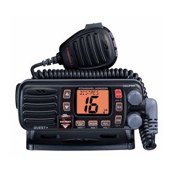
- Page 1 25 Watt VHF/FM Marine Transceiver QUEST GX1255S SERVICE MANUAL EM001N90A...
-
Page 2: Specifications
Specifications GENERAL Channels: All USA, International and Canadian Input Voltage: 13.8 VDC ±20% Current Drain: Standby 0.5 A Receive 1.5 A Transmit 5.0 A (Hi); 1.5 A (Lo) Dimensions: 2-1/2” H x 6-5/16” W x 6-5/16” D (64 H x 160 W x 160 D mm) Flush-Mount Dimensions: 2”... - Page 3 ExplodCircuit Descriptioned View & Miscellaneous Parts RA0458700 (BLACK) SLEEVE ASSY BK ƒ RA0422500 (WHITE) SLEEVE ASSY ƒ RA0422700 RUBBER PACKING FRONT ƒ RA0421500 (x 2pcs) O RING (SCREW) P1091158 MR-S AM001N ‚ ‚ ƒ RA0422900 O RING M CONECT RA0423000 HOLDER PLATE PWR „...
- Page 4 Note...
- Page 5 Block Diagram...
- Page 6 Connection Diagram...
-
Page 7: Circuit Description
Circuit Description Reception and transmission are switched by “RX-CNTL” PLL Synthesizer and “TX-CNTL” lines from the CNTL Unit. The receiver The 1st LO maintains stability from the PLL synthesizer uses double-conversion superheterodyne circuitry, with by using a 21.850 MHz reference signal from crystal X1001. a 21.4 MHz 1st IF and 450 kHz 2nd IF. -
Page 8: Dsc Encoder/ Decoder
Circuit Description lers Q1004 (2SA1602A), Q1008 (2SC4154E) and Q1012 1050 Hz Weather Alert Decoder (2SA1602A) to transmitter RF power amplifier Q1001, 1050Hz Weather Alert signals are demodulated on the thus providing positive control of the power output. CNTL Unit, and are applied to low-pass filter Q1026 (2SC4154E), and pass thorugh the limiter comparator Generation of spurious products by the transmitter is min- Q1028 (NJM2902M). -
Page 9: Required Test Equipment
Also, Standard Horizon, and that this temperature be held constant between 68 °F a division of VERTEX STANDARD, must reserve the right and 86 °F (20 °C and 30 °C). -
Page 10: Overview Of Test Mode
Alignment Overview of Test Mode Confirmation of VCO The test mode has been build in the microprocessor in or- — Confirmation — der to adjust and comfirm the performance of transceiver. r Connect the DC voltmeter to the test point (TP1019). r Use the [ p ( UP )] / [ q ( DOWN )] key to set the channel The purpose is to adjust transceiver simply and to con- to EXP04, confirm that voltage on the test point is... -
Page 11: Adjustment Of Pll Frequency
Alignment — Confirmation — — Confirmation — r Use the [ H/L ] key to set transceiver to high power r Set the output of the AG to 1 kHz and 150 mV. r Set the channel to EXP01, confirm that maximum and set the channel to EXP01. -
Page 12: Confirmation Of Weather Alert Tone
Alignment Confirmation of Weather Alert Tone Confirmation of DSC Operation In the weather channel mode, when transceiver receives — Confirmation — the specific emergency tone (1050 Hz), weather alert tone r Prepare the confirmation transceiver (GX1260S). will be output (Weather Alert Operation). The Weather r Input below data to the confirmation transceiver in Alert mode will be active when a NOAA weather chan- advance. -
Page 13: Main Unit
MAIN Unit Circuit Diagram RX: –10.6 dBµ RX: –7.0 dBµ (21.4 MHz) RX: 7.7 V RX: 7.5 V RX: 1.9 V RX: 1.2 V RX: +3.0 dBµ TX: 0.8 V RX: –8.0 dBµ RX: 4.7 V RX: 1.0 V SQL ON: 4.8 V RX: 7.9 V RX: 0.5 V RX: 1.2 V... - Page 14 MAIN Unit MAIN Unit Note...
- Page 15 MAIN Unit Parts Layout RA35H1516 LA4425A NJM7808FA (Q1001) (Q1031) (Q1002) LV2105V NJM12902V NJM2904V (Q1017) (Q1028) (Q1034) TA31136FN (Q 1024) NJM78M05 2SK210GR (YG) 3SK320 (U7) (Q1003) (Q1020) (Q1018) 2SA1602A (MF) 2SC3357 (MF) RT1N241M (N2) (Q1007) (Q1011) (Q1029, 1033) RT1N441U (M3) 2SC4154 (LE) DTB123EK (F52) (Q1005, 1009, 1010, (Q1025, 1026)
- Page 16 MAIN Unit Parts Layout NJM2212M 2SA1162GR (SG) 2SC2712GR (LG) (Q1032) (Q1036) (Q1037) 2SC4154 (LE) (Q1015) 2SC4400 (RT4) (Q1022) 2SC5006 (24) (Q1014) 1SS321 (F9) HZM5.6MB2 (D1002) (Q1032) DAN235U (M) (D1006) Side B...
-
Page 17: Parts List
MAIN Unit Parts List DESCRIPTION VALUE TOL. MFR'S DESIG VXSTD P/N VERS. LOT SIDE LAY ADR PCB with Components CB2155001 Printed Circuit Board AM001N000 FR008500C C 1001 CHIP CAP. 0.001uF GRM39B102K50PT K22174821 C 1002 CERAMIC CAP. 12pF CHU5 120J6 K02179103 C 1004 CERAMIC CAP. - Page 18 MAIN Unit Parts List DESCRIPTION VALUE TOL. MFR'S DESIG VXSTD P/N VERS. LOT SIDE LAY ADR C 1104 CHIP CAP. 0.01uF GRM39B103M50PT K22174823 C 1107 CHIP TA.CAP. 10uF 6.3V TEMSVA0J106M-8R K78080027 C 1109 CHIP CAP. GRM39CH070D50PT K22174208 C 1110 CHIP CAP. 0.001uF GRM39B102K50PT K22174821...
- Page 19 MAIN Unit Parts List DESCRIPTION VALUE TOL. MFR'S DESIG VXSTD P/N VERS. LOT SIDE LAY ADR C 1217 CHIP TA.CAP. 10uF TEMSVA1A106M-8R K78100028 C 1218 CHIP CAP. GRM39CH080D50PT K22174209 C 1219 CHIP CAP. 0.1uF GRM39B104K16PT K22124805 C 1220 CHIP CAP. 0.001uF GRM39B102K50PT K22174821...
- Page 20 MAIN Unit Parts List DESCRIPTION VALUE TOL. MFR'S DESIG VXSTD P/N VERS. LOT SIDE LAY ADR Q 1027 TC4S66F TE85R G1090893 Q 1028 NJM12902V(TE1) G1093592 Q 1029 TRANSISTOR RT1N241M-T11-1 G3070249 Q 1030 TC4S66F TE85R G1090893 Q 1031 LA4425A G1092241 Q 1032 NJM2211M(TE1) G1092943 Q 1033...
- Page 21 MAIN Unit Parts List DESCRIPTION VALUE TOL. MFR'S DESIG VXSTD P/N VERS. LOT SIDE LAY ADR R 1080 CHIP RES. 1/16W RMC1/16 103JATP J24185103 R 1081 CHIP RES. 1/16W RMC1/16 102JATP J24185102 R 1082 CHIP RES. 1/16W RMC1/16 333JATP J24185333 R 1083 CHIP RES.
- Page 22 MAIN Unit Parts List DESCRIPTION VALUE TOL. MFR'S DESIG VXSTD P/N VERS. LOT SIDE LAY ADR T 1002 COIL MC120 E526HNSA-110461 L0190261 T 1003 COIL MC120 E526HNSA-110462 L0190262 T 1004 COIL MC120 E526HNSA-110462 L0190262 T 1005 COIL MC120 E526HNSA-110461 L0190261 TC1001 TRIMMER CAP.
- Page 23 CNTL Unit Circuit Diagram LCD Contrast: 3.8 ~ 5.0 V 2.45 V (@13.8V) Dimmer Control: 0 ~ 6.1 V Dimmer Control: 0 ~ 4.8 V Key Beep: 500 mVp-p Weather Alert: 2.5 Vp-p Distress Alert: 5.0 Vp-p MAX. 5.0 Vp-p 3.0 Vp-p 4.0 Vp-p PTT “ON”: 0 V...
- Page 24 CNTL Unit Note...
-
Page 25: Cntl Unit
CNTL Unit Parts Layout DS2001 SEGMENT Side A DS2001 COMMON... - Page 26 CNTL Unit Parts Layout M37560EFGP BR24C62F 2SC4154 (LE) (Q2004) (Q2007) (Q2002, 2008) CPH6102 () PST597CNR (7C) RT1N241M (N2) (Q2009) (Q2005) (Q2003) MC2850 (A7) (D2008) Side B...
- Page 27 CNTL Unit Parts List DESCRIPTION VALUE TOL. MFR'S DESIG VXSTD P/N VERS. LOT SIDE LAY ADR PCB with Components CB2156001 Printed Circuit Board AM001N000 FR0085100 C 2003 CHIP CAP. 0.001uF GRM39B102K50PT K22174821 C 2005 CHIP CAP. 0.01uF GRM39B103M50PT K22174823 C 2007 CHIP CAP.
- Page 28 CNTL Unit Parts List DESCRIPTION VALUE TOL. MFR'S DESIG VXSTD P/N VERS. LOT SIDE LAY ADR R 2039 CHIP RES. 1/16W RMC1/16 101JATP J24185101 R 2040 CHIP RES. 1/16W RMC1/16 101JATP J24185101 R 2041 CHIP RES. 4.7k 1/16W RMC1/16 472JATP J24185472 R 2042 CHIP RES.
-
Page 29: Circuit Diagram
VR Unit Circuit Diagram Parts Layout Side A Side B Parts List DESCRIPTION VALUE TOL. MFR'S DESIG VXSTD P/N VERS. LOT SIDE LAY ADR PCB with Components CB2157001 Printed Circuit Board AM001N000 FR0085200 J 3001 WIRE ASSY AM001N T9207014 VR3001 POT. RK0971111 20KA/SW J60800262 VR3002 POT. - Page 30 MIC Unit Circuit Diagram Parts Layout Side A Side B Parts List DESCRIPTION VALUE TOL. MFR'S DESIG VXSTD P/N VERS. LOT SIDE LAY ADR C 4001 CERAMIC CAP. 0.001uF UP050B102K-A-B K28179001 D 4001 DIODE RD4.7EB2 G2090158 MC4001 MIC. ELEMENT EM-100PT M3290029 R 4001 CARBON FILM RES.
- Page 32 © 2000 VERTEX STANDARD CO., LTD. All rights reserved. Marine Division of VERTEX STANDARD No portion of this manual may be reproduced US Headquarters without the permission of 17210 Edwards Rd., Cerritos, CA 90703, U.S.A. VERTEX STANDARD CO., LTD. Printed in Japan. 0012K-0Y...