Sony PRS-505 Service Manual
Portable reader system
Hide thumbs
Also See for PRS-505:
- User manual (190 pages) ,
- Quick start manual (10 pages) ,
- Specifications (2 pages)
Table of Contents
Advertisement
Quick Links
QQ
3 7 63 1515 0
SERVICE MANUAL
Ver. 1.1 2007.12
• SONY and the SONY logo are registered trademarks of Sony Corporation.
• BBeB, BBeB Book, and their logos are trademarks of Sony Corporation.
• "Memory Stick," "Memory Stick Duo," "Memory Stick PRO Duo," and their logos are trademarks of Sony Corporation.
• Bitstream is a registered trademark, and Dutch, Font Fusion, and Swiss are trademarks, of Bitstream Inc.
• Microsoft, Windows, Windows Vista and Windows Media are trademarks or registered trademarks of Microsoft Corporation
in the United States and / or other countries.
• Adobe, Adobe Reader and Adobe PDF are trademarks or registered trademarks of Adobe Systems Incorporated in the United
States and/or other countries.
• MPEG Layer-3 audio coding technology and patents licensed from Fraunhofer IIS and Thomson.Continued 90 US
• This product uses MontaVista Software, Inc.'s MontaVista(R) Linux(R) Professional Edition as the operating system.
TE
L 13942296513
COPYRIGHT ©1999-2006 MONTAVISTA SOFTWARE, INC. ALL RIGHTS RESERVED.
http://www.mvista.com/
• MontaVista is a registered trademark of MontaVista Software, Inc.
• This product includes software developed by the OpenSSL Project for use in the OpenSSL Toolkit. (<http://www.openssl.
org/>) Copyright © 1998-2006 The OpenSSL Project. All rights reserved. This product includes cryptographic software
written by Eric Young (eay@cryptsoft.com). This product includes software written by Tim Hudson (tjh@cryptsoft.com).
For details on OpenSSL License, refer to "openssl.txt" on the CD-ROM.
All other system names and product names appearing in this document are generally the registered trademarks or trademarks
of their respective manufacturers. Further, the trademark TM and registered trademark ® symbols are not indicated throughout
this document.
Program ©2006, 2007 Sony Corporation
Documentation ©2006, 2007 Sony Corporation
www
.
Sony Corporation
9-887-835-02
2007L05-1
Audio Business Group
©
2007.12
Published by Sony Techno Create Corporation
http://www.xiaoyu163.com
x
ao
u163
y
i
http://www.xiaoyu163.com
PRS-505
2 9
8
Power source
Built-in rechargeable battery: DC 3.7 V
AC power adapter: DC 5.2 V
Battery life (continuous playback)
Approx. 7500 pages (when the battery is fully charged)
Q Q
User available capacity
3
6 7
1 3
1 5
Approx. 192MB
Available storage capacity of the Reader may vary.
Operating temperature
5 to 35 °C (41 to 95 °F)
Dimensions (w/h/d)
Approx. 6.9 × 4.8 × 0.3 inches (maximum, without soft cover)
Mass
Approx. 9 oz (without soft cover)
Package Contents
The Reader comes installed with a built-in rechargeable
battery.
• Reader (with Soft cover) (1)
• USB cable (1)
• CD-ROM (1)
- eBook Library software
- User's Guide (PDF)
- Sample contents
• Quick Start Guide (this manual) (1)
• Flyers
• Dummy cards (2)
Note
• This CD-ROM will not play in an audio CD player.
Design and specifi cations are subject to change without notice.
PORTABLE READER SYSTEM
co
.
9 4
2 8
US Model
Canadian Model
SPECIFICATIONS
0 5
8
2 9
9 4
2 8
m
9 9
9 9
Advertisement
Table of Contents

Related Manuals for Sony PRS-505


Summary of Contents for Sony PRS-505
- Page 1 SPECIFICATIONS • BBeB, BBeB Book, and their logos are trademarks of Sony Corporation. • “Memory Stick,” “Memory Stick Duo,” “Memory Stick PRO Duo,” and their logos are trademarks of Sony Corporation. Power source • Bitstream is a registered trademark, and Dutch, Font Fusion, and Swiss are trademarks, of Bitstream Inc.
-
Page 2: Table Of Contents
LES DIAGRAMMES SCHÉMATIQUES ET LA LISTE DES PIÈCES SONT CRITIQUES POUR LA SÉCURITÉ DE FONC- TIONNEMENT. NE REMPLACER CES COM- POSANTS QUE PAR DES PIÈCES SONY DONT LES NUMÉROS SONT DON- NÉS DANS CE MANUEL OU DANS LES SUPPLÉMENTS PUBLIÉS PAR SONY. -
Page 3: Servicing Notes
IC1203 • Copy the LUT fi le you want to update to the folder under “/ Sony Reader/software” in the memory stick or SD memory How to check the version of the stored LUT: • When you insert the memory stick or SD memory card in card exclusive for the test mode, and then change the name to which the exclusive fi... - Page 4 • Removing the soft cover FLASH ROM (IC1203) is replaced, you need to change the LUT. Pull the tab of soft cover towards Remove Sony’s Reader in the direction of • Attaching the soft cover Insert the tab of the soft cover in the hole of Sony’s...
-
Page 5: General
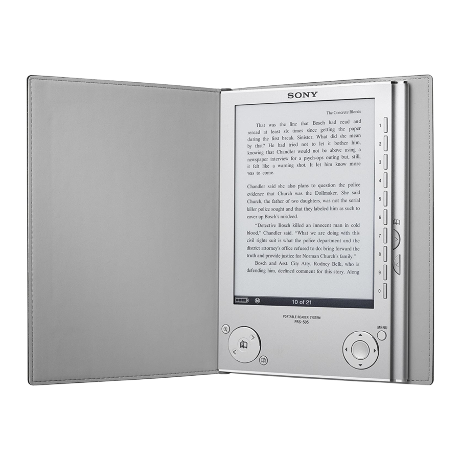
PRS-505 SECTION 2 This section is extracted GENERAL from instruction manual. 3 7 63 1515 0 Guide to Parts and Controls Holes for soft cover attachment The soft cover is attached when purchased. Folds open in use Note •... -
Page 6: Disassembly
PRS-505 SECTION 3 DISASSEMBLY 3 7 63 1515 0 • This set can be disassembled in the order shown below. 3-1. DISASSEMBLY FLOW Note 1: The process described in can be performed in any order. Note 2: Without completing the process described in , the next process can not be performed. -
Page 7: Ornamental Plate (Lower) Assy
PRS-505 3 7 63 1515 0 3-3. ORNAMENTAL PLATE (LOWER) ASSY screw (M1.4) ornamental plate (lower) assy claw two claws The lower part of the back side two screws (M1.4) L 13942296513 3-4. MAIN ASSY connector (CN801) spacer (CON_key) Please open the lower side of case assy a little up and down. -
Page 8: Ion) Storage Battery Assy
PRS-505 3 7 63 1515 0 3-5. (ION) STORAGE BATTERY ASSY two screws (M1.4) (ion) storage battery assy upper side main assy back side lower side connector (CN401) L 13942296513 3-6. SLOT FLEXIBLE BOARD two screws (M1.4) connector (CN201) -
Page 9: Connect Flexible Board
PRS-505 3 7 63 1515 0 3-7. CONNECT FLEXIBLE BOARD two screws (M1.4) spacer (CON_USB) CONNECT FLEXIBLE board connector (CN901) adhesive sheet (D) Note: When peeling off adhesive sheet, upper side be sure to exchange it for new adhesive sheet. -
Page 10: Main Board, Ink (Indication) Element Assy (Iie1)
PRS-505 3 7 63 1515 0 3-9. MAIN BOARD, INK (INDICATION) ELEMENT ASSY (IIE1) screw (M1.4 × 2) MAIN board connector (CN302) ink (indication) element assy (IIE1) L 13942296513 u163 http://www.xiaoyu163.com... -
Page 11: Test Mode
1. Ready for the SD memory card or memory stick. adjustment is required when replacing a board or panel. 2. Make the new directly as “/Sony Reader/software” on the SD TEST MODE MENU is changed to “Done” from “Not Yet”. -
Page 12: Diagrams
PRS-505 SECTION 6 DIAGRAMS 3 7 6 3 1 5 1 5 0 6-1. BLOCK DIAGRAM - MAIN Section (1/2) - CN201 23 – D0 – D15 MS-DATA0 – 70, 72, MSDAT0 – BD0 – BD15 DATA BUS D0 – D31 D0 –... -
Page 13: Block Diagram - Main Section (2/2)
PRS-505 3 7 6 3 1 5 1 5 0 6-2. BLOCK DIAGRAM - MAIN Section (2/2) - SSI_TXDAT F9 SDATA HPL 23 J002 SSI_TXCLK A8 BICK HPR 22 SSI_TXFS C8 LRCK AUDIO3_DATA A1 CDTI AUDIO2_CLK B2 CCLK AUDIO1_CS B1... -
Page 14: Block Diagram - Key/Power Supply Section
PRS-505 3 7 6 3 1 5 1 5 0 6-3. BLOCK DIAGRAM - KEY/POWER SUPPLY Section - USBBOOT 52 USB_BOOT USBCHG 46 USB_CHRG RXD 58 UART1_TXD TXD 59 UART1_RXD RTS 57 UART1_RTS CTS 42 UART1_CTS SWITCHING S873 POR 22 REGULATOR VOL −... -
Page 15: Main Board (Component Side)
PRS-505 3 7 6 3 1 5 1 5 0 THIS NOTE IS COMMON FOR PRINTED WIRING BOARDS AND SCHEMATIC DIAGRAMS. • Waveforms – MAIN Board – (In addition to this, the necessary note is printed in each block.) IC107 For Printed Wiring Boards. - Page 16 PRS-505 3 7 6 3 1 5 1 5 0 6-4. PRINTED WIRING BOARD - MAIN Board (Component Side) - • : Uses unleaded solder. FLEXIBLE MAIN BOARD CONNECT (Page 28) BOARD (COMPONENT SIDE) FLEXIBLE BOARD C111 C123 R1298...
-
Page 17: Main Board (Conductor Side)
PRS-505 3 7 6 3 1 5 1 5 0 6-5. PRINTED WIRING BOARD - MAIN Board (Conductor Side) - • : Uses unleaded solder. MAIN BOARD (CONDUCTOR SIDE) TP1566 TP1569 TP1577 TP1584 TP2003 TP2005 TP1512 TP816 TP814 TP810... -
Page 18: Schematic Diagram - Main Board (1/10)
PRS-505 3 7 6 3 1 5 1 5 0 6-6. SCHEMATIC DIAGRAM - MAIN Board (1/10) - • See page 29 for IC Block Diagram. • See page 34 for IC Pin Function Description. PCR5CCLK (1/10) SDDET SDWP... -
Page 19: Schematic Diagram - Main Board (4/10)
PRS-505 3 7 6 3 1 5 1 5 0 6-7. SCHEMATIC DIAGRAM - MAIN Board (2/10) - • See page 15 for waveform. • See page 29 for IC Block Diagram. (2/10) SRDSP STXD STCK STFS (Page 23) -
Page 20: Schematic Diagram - Main Board (6/10)
PRS-505 3 7 6 3 1 5 1 5 0 6-8. SCHEMATIC DIAGRAM - MAIN Board (3/10) - • See page 29 for IC Block Diagram. (3/10) 8-15V 8+15V R1882 8-V3 UNREG (Page 21) (Page 21) Q1814 HN1B04FE-Y/GR R1802... -
Page 21: Schematic Diagram - Main Board (4/10)
PRS-505 3 7 6 3 1 5 1 5 0 6-9. SCHEMATIC DIAGRAM - MAIN Board (4/10) - • See page 29 for IC Block Diagram. • See page 34 for IC Pin Function Description. (4/10) 8-V3 C312 R385... -
Page 22: Schematic Diagram - Main Board (8/10)
PRS-505 3 7 6 3 1 5 1 5 0 6-10. SCHEMATIC DIAGRAM - MAIN Board (5/10) - • See page 15 for waveform. • See page 29 for IC Block Diagram. (5/10) TP1544 BEB2 TP1545 L1202 C1221 (Page 18) 22μH... -
Page 23: Schematic Diagram - Main Board (9/10)
PRS-505 3 7 6 3 1 5 1 5 0 6-11. SCHEMATIC DIAGRAM - MAIN Board (6/10) - • See page 15 for waveform. • See page 29 for IC Block Diagram. • See page 34 for IC Pin Function Description. -
Page 24: Schematic Diagram - Main Board (10/10)
PRS-505 3 7 6 3 1 5 1 5 0 6-12. SCHEMATIC DIAGRAM - MAIN Board (7/10) - • See page 15 for waveform. • See page 34 for IC Pin Function Description. (7/10) (Page 27) LED-VCC TP806 L801... -
Page 25: Schematic Diagram - Main Board (8/10)
PRS-505 3 7 6 3 1 5 1 5 0 6-13. SCHEMATIC DIAGRAM - MAIN Board (8/10) - (8/10) (Page 27) A(24-0) A(24-0) C1219 C1218 L1201 TP1201 22μH (Page 26) D(31-0) D(31-0) (Page 23) SDCLK DQM0 DQM1 DQM2 DQM3... -
Page 26: Schematic Diagram - Main Board (9/10)
PRS-505 3 7 6 3 1 5 1 5 0 6-14. SCHEMATIC DIAGRAM - MAIN Board (9/10) - • See page 29 for IC Block Diagram. (9/10) BD(31-0) BA(24-0) A(24-0) (Page 22) L1101 C1112 C1101 22μH C1103 D(31-0) (Page 25) - Page 27 PRS-505 3 7 6 3 1 5 1 5 0 6-15. SCHEMATIC DIAGRAM - MAIN Board (10/10) - • See page 29 for IC Block Diagram. • See page 34 for IC Pin Function Description. (10/10) ISET2 STAT2 BATT-DC...
-
Page 28: Printed Wiring Board
PRS-505 3 7 6 3 1 5 1 5 0 6-16. PRINTED WIRING BOARD - CONNECT FLEXIBLE Board - 6-17. SCHEMATIC DIAGRAM - CONNECT FLEXIBLE Board - • : Uses unleaded solder. CONNECT FLEXIBLE BOARD CN006 (USB) MAIN BOARD... - Page 29 PRS-505 3 7 63 1515 0 • IC Block Diagrams – MAIN Board – IC101 AK4365VN-L 26 25 24 23 22 SERIAL MCLK CDTI INTERFACE CCLK HEADPHONE CONVERTER (L-ch) 21 HPGND LRCK BUFFER AUDIO BICK CONVERTER 20 HPVCC INTERFACE...
- Page 30 PRS-505 3 7 63 1515 0 IC204, 205, 409 XC6213B312NR ON/OFF CE 1 CONTROL VOUT CURRENT LIMIT – VOLTAGE REFERENCE VSS 2 IC302 XC6215B152NR IC303 XC6215B312NR IC406 XC6215B292NR ON/OFF EACH CIRCUIT CONTROL ERROR AMP VOLTAGE – CURRENT REFERENCE LIMIT...
- Page 31 PRS-505 3 7 63 1515 0 IC407 TC7WH74FK(TE85R) IC953 S1R72V17B00A20B G7 B7 B6 B5 B4 B2 D7 G2 C7 A7 A2 C2 B3 A5 OSCILLATOR FIRST-IN FIRST-OUT TESTEN TEST CD15 ATPGEN FIRST-IN FIRST-OUT CD14 CONTROLLER BURNIN CD13 CD12 CD11...
- Page 32 PRS-505 3 7 63 1515 0 IC1101, 1102 TC7MP245FK (EL) A5 6 A6 7 L 13942296513 A7 8 A8 9 GND 10 IC1112, 1113 SN74LVC244APWR u163 http://www.xiaoyu163.com...
- Page 33 PRS-505 3 7 63 1515 0 IC1802 LT3467ES6#TR 1.255V DRIVER COMPARATOR REFERENCE – – SHUTDOWN SHDN – RAMP GENERATOR 1.3MHz OSCILLATOR IC1805 LT1931ES5#TR LATCH L 13942296513 RAMP GENERATOR 1.2MHz OSCILLATOR SHDN IC1806 TC7W53FK (TE85R) COMMON 1 INH 2 VEE 3...
- Page 34 PRS-505 3 7 63 1515 0 • IC Pin Function Description MAIN BOARD IC201 R5C807 (MEMORY STICK DUO/SD MEMORY CARD CONTROLLER) Pin No. Pin Name Description VCCEN +3.3V power supply control signal output terminal Not used GPIO Not used...
- Page 35 PRS-505 3 7 63 1515 0 Pin No. Pin Name Description Ground terminal 91, 92 SDDAT0, SDDAT1 Two-way 4-bits data bus with the SD memory card slot MSBS Bus state signal output to the memory stick duo slot SDDAT2...
- Page 36 PRS-505 3 7 63 1515 0 MAIN BOARD IC301 A3P125-VQG100 (INDICATOR CONTROLLER) Pin No. Pin Name Description Ground terminal 2 to 8 PD15 to PD9 Video data input from the main CPU Ground terminal 10, 11 PD8, PD7 Video data input from the main CPU...
- Page 37 PRS-505 3 7 63 1515 0 Pin No. Pin Name Description I2CSCL Not used I2CSDA Not used PWR3 Not used RESERVED Not used 84 to 86 TEST2 to TEST0 Ground terminal VCCIB Power supply terminal (+3.3V) Ground terminal Power supply terminal (+1.5V)
- Page 38 PRS-505 3 7 63 1515 0 MAIN BOARD IC401 SN412005RHLR (CHARGE CONTROL) Pin No. Pin Name Description Power supply (+3.3V) output terminal STAT1 Charge state signal output to the sub CPU and LED drive signal for CHARGE indicator STAT2...
- Page 39 PRS-505 3 7 63 1515 0 MAIN BOARD IC801 HD64F38004FP10V-V198 (SUB CPU) Pin No. Pin Name Description BATT-DC Power supply input from the AC adaptor System clock input terminal (32.768 kHz) System clock output terminal (32.768 kHz) Ground terminal OSC2 System clock output terminal (4.9152 MHz)
- Page 40 PRS-505 3 7 63 1515 0 MAIN BOARD IC1001 MC9328MXLVP20R2 (MAIN CPU) Pin No. Pin Name Description AUDIO3_DATA Serial data output to the audio D/A converter SRAMINT Not used VBUS VBUS input from the USB connector XUSBD_OE USB output enable signal output terminal...
- Page 41 PRS-505 3 7 63 1515 0 Pin No. Pin Name Description UART1_RXD Serial data input from the sub CPU UART1_CTS Clear to send signal output to the sub CPU NAND-CLE Command latch enable signal output to the NAND fl ash mamory...
- Page 42 PRS-505 3 7 63 1515 0 Pin No. Pin Name Description NVDD1 Power supply terminal (+2.9V) K6, K7 Ground terminal NVDD1 Power supply terminal (+2.9V) Ground terminal Two-way data bus with the memory stick duo/SD memory card controller, USB controller, NAND fl...
- Page 43 PRS-505 3 7 63 1515 0 Pin No. Pin Name Description DQM1 Data enable signal output to the SD-RAM XRAS Row address select signal output to the SD-RAM SDCKE1 Clock enable signal output to the SD-RAM Not used CLKO...
-
Page 44: Exploded Views
PRS-505 SECTION 7 EXPLODED VIEWS 3 7 63 1515 0 Note: • -XX and -X mean standardized parts, so • The mechanical parts with no reference • Accessories are given in the last of the they may have some difference from the number in the exploded views are not sup- electrical parts list. -
Page 45: Main Section
PRS-505 Ver. 1.1 3 7 63 1515 0 7-2. MAIN SECTION IIE1 L 13942296513 Note: When peeling off adhesive sheet, be sure to exchange it for new adhesive sheet. Ref. No. Part No. Description Remark Ref. No. Part No. - Page 46 PRS-505 SECTION 8 CONNECT FLEXIBLE MAIN ELECTRICAL PARTS LIST 3 7 63 1515 0 Note: • Due to standardization, replacements in • COILS When indicating parts by reference num- the parts list may be different from the uH: μH ber, please include the board name.
- Page 47 PRS-505 MAIN 3 7 63 1515 0 Ref. No. Part No. Description Remark Ref. No. Part No. Description Remark C406 1-100-672-11 CERAMIC CHIP 10uF C1012 1-125-777-11 CERAMIC CHIP 0.1uF C407 1-127-760-11 CERAMIC CHIP 4.7uF 6.3V C1013 1-125-777-11 CERAMIC CHIP 0.1uF...
- Page 48 PRS-505 MAIN 3 7 63 1515 0 Ref. No. Part No. Description Remark Ref. No. Part No. Description Remark C1812 1-165-887-91 CERAMIC CHIP 0.22uF 6.3V IC403 6-711-801-01 IC XC9226A196MR C1814 1-100-162-91 CERAMIC CHIP 1uF C1816 1-164-005-11 CERAMIC CHIP 0.47uF...
- Page 49 PRS-505 MAIN 3 7 63 1515 0 Ref. No. Part No. Description Remark Ref. No. Part No. Description Remark < FUSE > R250 1-400-827-31 BEAD, FERRITE (1005) R251 1-400-827-31 BEAD, FERRITE (1005) 0 PS401 1-576-415-21 FUSE (2A/32V) R252 1-218-990-81...
- Page 50 PRS-505 MAIN 3 7 63 1515 0 Ref. No. Part No. Description Remark Ref. No. Part No. Description Remark R429 1-220-804-11 RES-CHIP 2.2M 1/16W R1821 1-208-935-11 METAL CHIP 100K 0.5% 1/16W R430 1-218-977-11 RES-CHIP 100K 1/16W R1823 1-208-920-81 METAL CHIP 0.5%...
- Page 51 PRS-505 Ver. 1.1 MAIN SLOT FLEXIBLE 3 7 63 1515 0 Ref. No. Part No. Description Remark Ref. No. Part No. Description Remark R2215 1-218-965-11 RES-CHIP 1/16W X801 1-795-029-11 VIBRATOR, CRYSTAL (32.768kHz) R2216 1-218-965-11 RES-CHIP 1/16W X802 1-813-181-21 VIBRATOR, CERAMIC (4.9152MHz)
- Page 52 PRS-505 3 7 63 1515 0 MEMO L 13942296513 u163 http://www.xiaoyu163.com...
- Page 53 PRS-505 http://www.xiaoyu163.com PRS-505 1. NEW/FORMER DISCRIMINATION 3 7 6 3 1 5 1 5 0 – MAIN Board (Component Side) – US Model Canadian Model SERVICE MANUAL Former : 1-875-228-11 : 1-875-228-12 Ver. 1.1 2007.12 SUPPLEMENT-1 File this supplement with the service manual.
- Page 54 PRS-505 2. DIAGRAMS 3 7 6 3 1 5 1 5 0 THIS NOTE IS COMMON FOR PRINTED WIRING BOARDS AND SCHEMATIC DIAGRAMS. (In addition to this, the necessary note is printed in each block.) For Printed Wiring Boards.
- Page 55 PRS-505 3 7 6 3 1 5 1 5 0 2-1. PRINTED WIRING BOARD - MAIN Board (Component Side) - • : Uses unleaded solder. FLEXIBLE MAIN BOARD CONNECT (Refer to page BOARD (COMPONENT SIDE) FLEXIBLE 28 on orogonal...
- Page 56 PRS-505 3 7 6 3 1 5 1 5 0 2-2. PRINTED WIRING BOARD - MAIN Board (Conductor Side) - • : Uses unleaded solder. MAIN BOARD (CONDUCTOR SIDE) TP1566 TP1569 TP1577 TP1584 TP2003 TP2005 TP1512 TP816 TP814 TP810...
- Page 57 PRS-505 3 7 6 3 1 5 1 5 0 2-3. SCHEMATIC DIAGRAM - MAIN Board (1/10) - PCR5CCLK (1/10) SDDET SDWP PCSDCARD CLKO PCMSCARD (Page 10) MSDET L207 100μH PCR5C C207 C201 IC206 SRR5C ADDRESS TC7SZ125FU DECODER (Page 10)
- Page 58 PRS-505 3 7 6 3 1 5 1 5 0 2-4. SCHEMATIC DIAGRAM - MAIN Board (2/10) - (2/10) SRDSP STXD STCK STFS (Page 10) PCAUDIO AUDIO1 AUDIO2 AUDIO3 (Page 10) TP112 HP-R R120 HP-R C128 TP110 HP-L R122...
- Page 59 PRS-505 3 7 6 3 1 5 1 5 0 2-5. SCHEMATIC DIAGRAM - MAIN Board (3/10) - (3/10) 8-15V 8+15V R1882 8-V3 UNREG (Page 8) (Page 8) Q1814 HN1B04FE-Y/GR R1802 L1811 C1804 D1801 B− SWITCH 10μH BAT760-115 L1804...
- Page 60 PRS-505 3 7 6 3 1 5 1 5 0 2-6. SCHEMATIC DIAGRAM - MAIN Board (4/10) - (4/10) 8-V3 C312 R385 8-15V LCDBUS 8+15V (Page 7) R386 CN302 TP344 TP345 (Page 10) C313 TP346 TP319 C308 R378 R332...
- Page 61 PRS-505 3 7 6 3 1 5 1 5 0 2-7. SCHEMATIC DIAGRAM - MAIN Board (5/10) - (5/10) TP1544 BEB2 TP1545 L1202 C1221 (Page 5) 22μH VCORE TP1202 BD(31-0) C1220 BA(24-0) USBINT (Page USB20INT BA17 BA16 (Page 11)
- Page 62 PRS-505 2-8. SCHEMATIC DIAGRAM - MAIN Board (6/10) - 3 7 6 3 1 5 1 5 0 PCA3PIO (6/10) RB2016 PCA3PCORE 470k (Page 8) LCDBUS SRR5C SDINT PCR5C (Page 8) TP113 MSDET PA14 CLKO TP1515 (Page 5) R2105...
- Page 63 PRS-505 2-9. SCHEMATIC DIAGRAM - MAIN Board (7/10) - 3 7 6 3 1 5 1 5 0 (7/10) (Page 14) LED-VCC TP806 L801 C801 (Page SW-STBY STAT1 (Page 5) (Page STAT1 LED2-ORG (Page STAT1 TP860 R817 LED2-ORG DCDET...
- Page 64 PRS-505 3 7 6 3 1 5 1 5 0 2-10. SCHEMATIC DIAGRAM - MAIN Board (8/10) - (8/10) (Page 14) A(24-0) A(24-0) C1219 C1218 L1201 TP1201 22μH (Page 13) D(31-0) D(31-0) (Page 10) SDCLK DQM0 DQM1 DQM2 DQM3...
- Page 65 PRS-505 3 7 6 3 1 5 1 5 0 2-11. SCHEMATIC DIAGRAM - MAIN Board (9/10) - (9/10) BD(31-0) BA(24-0) A(24-0) (Page 9) L1101 C1112 C1101 22μH C1103 D(31-0) (Page 12) IC1101 IC1117 BUFFER TC7MP245FK(EL) TC7SZ125FU BUFFER TP1546...
- Page 66 PRS-505 3 7 6 3 1 5 1 5 0 2-12. SCHEMATIC DIAGRAM - MAIN Board (10/10) - (10/10) ISET2 STAT2 BATT-DC TP408 DCDET Q406 DCDET HN1B04FE-Y/GR Q402,405,406 R426 USBON B+ SWITCH (Page 11) PWRON R424 470k Q402 RTQ035P02TR...
- Page 67 PRS-505 MAIN 3. ELECTRICAL PARTS LIST 3 7 63 1515 0 Note: • Due to standardization, replacements in • COILS When indicating parts by reference num- the parts list may be different from the uH: μH ber, please include the board name.
- Page 68 PRS-505 MAIN 3 7 63 1515 0 Ref. No. Part No. Description Remark Ref. No. Part No. Description Remark C416 1-165-989-11 CERAMIC CHIP 10uF 6.3V C1018 1-165-989-11 CERAMIC CHIP 10uF 6.3V C417 1-165-989-11 CERAMIC CHIP 10uF 6.3V C1019 1-125-777-11 CERAMIC CHIP 0.1uF...
- Page 69 PRS-505 MAIN 3 7 63 1515 0 Ref. No. Part No. Description Remark Ref. No. Part No. Description Remark C1822 1-164-156-11 CERAMIC CHIP 0.1uF C1823 1-125-777-11 CERAMIC CHIP 0.1uF IC409 6-708-467-01 IC XC6213B312NR C1834 1-100-352-91 CERAMIC CHIP 1uF IC801...
- Page 70 PRS-505 MAIN 3 7 63 1515 0 Ref. No. Part No. Description Remark Ref. No. Part No. Description Remark Q402 6-550-354-01 TRANSISTOR RTQ035P02TR R303 1-218-990-81 SHORT CHIP Q403 6-550-254-01 TRANSISTOR 2SA1832F-GR (T3SOYF R322 1-218-985-11 RES-CHIP 470K 1/16W Q405 8-729-037-52 TRANSISTOR 2SD2216J-QR (TX).SO...
- Page 71 PRS-505 MAIN 3 7 63 1515 0 Ref. No. Part No. Description Remark Ref. No. Part No. Description Remark R802 1-218-965-11 RES-CHIP 1/16W R1829 1-208-683-11 METAL CHIP 0.5% 1/16W R803 1-218-941-81 RES-CHIP 1/16W R1832 1-208-683-11 METAL CHIP 0.5% 1/16W...
- Page 72 PRS-505 MAIN 3 7 63 1515 0 Ref. No. Part No. Description Remark Ref. No. Part No. Description Remark R2267 1-218-977-11 RES-CHIP 100K 1/16W R2268 1-218-977-11 RES-CHIP 100K 1/16W R2527 1-218-947-11 RES-CHIP 1/16W < COMPOSITION CIRCUIT BLOCK > RB201...
- Page 73 PRS-505 3 7 63 1515 0 MEMO L 13942296513 u163 http://www.xiaoyu163.com...
- Page 74 PRS-505 3 7 63 1515 0 REVISION HISTORY Checking the version allows you to jump to the revised page. Also, clicking the version at the top of the revised page allows you to jump to the next revised page.