
Related Manuals for Mitsubishi Diamond Pro 750SB


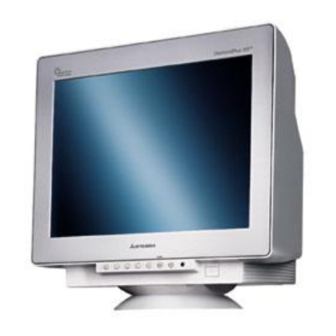
Summary of Contents for Mitsubishi Diamond Pro 750SB
-
Page 1: Service Manual
PART NO. 599910596 SERVICE MANUAL Diamond Pro 750SB COLOR MONITOR MODELS DPro 750SB (B)/-BK(B) NEC-MITSUBISHI ELECTRIC VISUAL SYSTEMS CORPORATION JUNE 2002 200207 08109705 08109730... - Page 2 WARNING The SERVICE PERSONNEL should have the appropriate technical training, knowledge and experience necessary to: • Be familiar with specialized test equipment, and • Be careful to follow all safety procedures associated with high voltage CRT circuit designs to minimize danger to themselves and their coworkers. To avoid electrical shocks, this equipment should be used with an appropriate power code and be connected only to a properly grounded AC outlet.
- Page 3 PRODUCT SAFETY CAUTION 1. When parts replacement is required for servicing, always use the manufacturer's specified replacement. 2. Comply with all caution and safety-related notes on the product display chassis and picture tube. 3. When replacing the component, always be certain that all the components are put back in the place. 4.
- Page 4 CONTENTS Page No. USER'S MANUAL ....................1-1 SERIAL NUMBER INFORMATION ............... 2-1 DISASSEMBLY ...................... 3-1 ADJUSTMENT PROCEDURES ................4-1 INSPECTION ......................5-1 TROUBLE SHOOTING ..................6-1 CIRCUIT DESCRIPTION ..................7-1 REPLACEMENT PARTS LIST ................8-1 BLOCK DIAGRAMS ....................9-1 SCHEMATIC DIAGRAMS ..................10-1...
- Page 5 User's Manual 1. B Version User’s Manual...
-
Page 6: Declaration Of The Manufacturer
686-1, Nishioi Oi-Machi Ashigarakami-gun Kanagawa 258-8533, Japan Product NERGY As an E Partner, NEC-Mitsubishi Electronics Display of America, Inc. has determined that this NERGY product meets the E guidelines for energy efficiency. The E emblem does not represent NERGY NERGY EPA endorsement of any product or service. - Page 7 WARNING TO PREVENT FIRE OR SHOCK HAZARDS, DO NOT EXPOSE THIS UNIT TO RAIN OR MOISTURE. ALSO, DO NOT USE THIS UNIT'S POLARIZED PLUG WITH AN EXTENSION CORD RECEPTACLE OR OTHER OUTLETS UNLESS THE PRONGS CAN BE FULLY INSERTED. EFRAIN FROM OPENING THE CABINET AS THERE ARE HIGH VOLTAGE COMPONENTS INSIDE. REFER SERVICING TO QUALIFIED SERVICE PERSONNEL.
- Page 8 Contents Your new Diamond Pro 750 / Diamond Plus 93 monitor box* should contain the following: • Diamond Pro 750 / Diamond Plus 93 Monitor with tilt/swivel base • Power Cord • Captive Signal Cable • User’s Manual • CD ROM with Setup Software, complete User’s Manual and other helpful files. To see the User’s Manual, Acrobat Reader 4.0 must be installed on your PC.
-
Page 9: Quick Start
Quick Start To attach the Diamond Pro 750 / Diamond Plus 93 monitor to your system, follow these instructions: 1. Turn off the power to your computer. 2. If necessary, install the display card into your system. For more information, refer to the display card manual. - Page 10 Quick Start – continued Power Outlet Power Cord Figure C.1 Power Button Figure D.1 6 User’s Manual...
-
Page 11: Size And Position Controls
Controls OSM (On-Screen Manager) control buttons on the front of the monitor function as follows: s t i s t i g i l g i l f e l r / t f e l r / t . s l –... -
Page 12: Geometry Controls
Controls – continued Color Control System Colour presets selects the desired colour setting. The bar is replaced by the colour setting choice. Each colour setting is adjusted at the factory to the stated Kelvin. If a setting is adjusted, the name of the setting will change from Kelvin to Custom except sRGB mode. - Page 13 Controls – continued Tools 2 Language: OSM controls menus are available in 6 languages. OSM Position: You can choose where you would like the OSM controls menu to appear on your screen. Selecting OSM Position allows you to manually adjust the OSM controls menu position from among Center, Top left, Top right, Bottom left and Bottom right.
-
Page 14: Recommended Use
Recommended Use Safety Precautions and Maintenance FOR OPTIMUM PERFORMANCE, PLEASE NOTE THE FOLLOWING WHEN SETTING UP AND USING THE DIAMOND PRO 750 / DIAMOND PLUS 93 COLOUR MONITOR: • DO NOT OPEN THE MONITOR. There are no user serviceable parts inside and opening or removing covers may expose you to dangerous shock hazards or other risks. - Page 15 Recommended Use – continued CORRECT PLACEMENT AND ADJUSTMENT OF THE MONITOR CAN REDUCE EYE, SHOULDER AND NECK FATIGUE. CHECK THE FOLLOWING WHEN YOU POSITION THE MONITOR: • Adjust the monitor height so that the top of the screen is at or slightly below eye level.
-
Page 16: Specifications
Specifications : l a ° 0 e l f e l l c t i e l l - i t l - i t c i t t n i i t i i t a c i t i t i i t a i t i... - Page 17 Specifications – continued : l a ° 0 e l f e l l c t i e l l - i t l i t n c i t t n i i t i i t a c i t i t i i t a i t i...
-
Page 18: User's Manual
The state-of-the-art Mitsubishi PX-DBF electron gun and tight 0.25 mm grille pitch delivers precise focus for crisp, clear text and images. -
Page 19: Trouble Shooting
Troubleshooting No picture • Display card should be completely seated in its slot. • Power Button and computer power switch should be in the ON position. • Signal cable should be completely connected to display card/computer. • Check connector for bent or pushed-in pins. Image is scrolling or unstable •... -
Page 20: Diamond Pro 750 Sb / Diamond Plus
TCO’99 Diamond Pro 750 / Diamond Plus 93 Congratulations! You have just purchased a TCO’99 approved and labeled product! Your choice has provided you with a product developed for professional use. Your purchase has also contributed to reducing the burden on the environment and also to the further develop- ment of environmentally adapted electronics products. - Page 21 TCO’99 – continued TCO’99 demand requires that plastic components weighing more than 25 grams must not contain flame retar- dants with organically bound chlorine and bromine. Flame retardants are allowed in the printed circuit boards since no substitutes are available. Lead** Lead can be found in picture tubes, display screens, solders and capacitors.
-
Page 22: Serial Number Information
Serial Number Information Refer to the serial number information shown below. EX.) SERIAL NUMBER LABEL Model : Dpro750SB : Dpro750SB-BK SERIAL NO. : g g g g g g g g g Manufactured Year : ( Last digit ) Manufactured Month : January to September 1 to 9 October... -
Page 23: Disassembly
DISASSEMBLY • Before you disassemble the set, turn off power and pull out the power plug. • Use the appropriate screwdrivers that first the screws. If you use screwdriver that does not fit, you may break the screws. • Assembly is the opposite process of Disassembly. •... - Page 24 CRT BOARD 1. Ten terminals are removed, and six solder is removed. terminals solder 2. Disconnect the connectors “S201”, “S202”, “S203” and “GND”. 3. Unsolder the wires “White wire”, “Red wire” and “G2”. S202 S201 S203 Red wire White wire...
- Page 25 MAIN BOARD 1. Disconnect the connectors “S102”, “S701” and “GND”. 2. Remove the screw (P-#2CRBITS*3*8*15BF). Screw S701 S101 3. Remove the two screws (P-#2CRBITS*3*8*15BF), screw (PL-CPTS*3*8*15BF) and screw (PL-CPIMS*4*10*15BF). Screw (P-#2CRBITS*3*8*15BF) Screw Screw (PL-CPIMS*4*10*15BF) (PL-CPTS*3*8*15BF)
- Page 26 4. Disconnect the connectors “GND” and “S301”. 5. Remove the screw (P-#2CRBITS*3*8*15BF) and the screw (PL-CPTS*3*8*15BF). 6. Remove the Anode cap from CRT. NOTE: Carefully discharge the CRT anode by shorting it to ground before removing anode cap. Screw GND S301 Screw 7.
- Page 27 8. Remove the eight screws (PL-CPTS*3*8*15BF) and remove the Main Board from Chassis Base. screw (PL-CPTS*3*8*15BF)
-
Page 28: Table Of Contents
ADJUSTMENT PROCEDURES TABLE OF CONTENTS Page 1. Adjustment & Inspection Tools.................... 4-2 2. Timing Table ........................4-2 3. Normal Condition Definition ....................4-2 4. Hot Key Operation ......................4-3 5. B+ Check ........................... 4-5 6. X-RAY Test ........................4-5 7. H. V. B+ Confirmation ......................4-5 8. -
Page 29: Adjustment & Inspection Tools
1. Adjustment & Inspection Tools (A) Color Analyzer (B) Signal Generator CHROMA 2235 or compatible (C) Multi Meter (D) Hi-Voltage Probe (E) Convergence Meter (F) Degaussing Probe (G) Power Meter 2. Timing Table (Factory Mode –18 Modes) MODE RESOLUTION H-SYNC EREQ. V-SYNC FREQ H . POLARITY V . POLARITY VGA400 31.4KHz 70Hz... -
Page 30: Hot Key Operation
4. Hot Key Operation (A) Factory Mode: power on + ‘+’ key + ‘−‘ key. *To hide the Factory menu temporary in Factory mode: Push "RESET" key once while Menu is displayed, then Menu disappears. Push "RESET" key once more, then Menu reappears. (B) Factory Menu TAB 1) BRIGHTNESS / CONTRAST : Brightness... - Page 31 TAB 5) TOOLS 1 :Moire canceller :Linearity(VER.) :Linearity balance TAB 6) TOOLS 2 TOOL 2 is as same as user mode TAB 7) INFORMATION DS :Destination...
-
Page 32: B+ Check
7. H. V. B+ Confirmation (A) Mode: No.12 (B) Pattern: Full Black (Brightness just cut off) (C) Adjust VR301 to make the high voltage has 25kV ±0.1kV for Mitsubishi CRT, 26kV ±0.1kV for Samsung CRT. 8. H-Raster Center Adjustment (A) Mode: No.13 (B) Pattern: Crosshatch Reverse (C) Adjust the Brightness Control so that the background is visible. -
Page 33: White Balance Adjustment
11. White Balance adjustment (A) Setting Enter Factory Mode, Mode: No.12, Pattern: Full White. Warm up 60 min. Make External Degauss. (B) Cut Off Adjustment 1. Select the color Mode 9300K. 2. Cut Off Adjustment : Video Signal Off(0.Vp-p),Bright Control set to Max., Adjust G. Bias at the Brightness 3.4 ±0.7cd/m (1FL ±0.2FL). - Page 34 2. 5000K (Select color Mode 5000K) 1) Video Signal off (0.Vp-p), Contrast set to Max, Adjust Brightness to 0.1cd/m 2) 50*50mm Green block Pattern, Adjust G Gain to Y=71cd/m 3) 50*50mm White block Pattern, Adjust R, B Gain to x=0.345, y=0.359. 4) Adjust R, G, B gain again to meet following spec.
-
Page 35: Focus Adjustment
12. Focus Adjustment (A) Mode: No.12, 9300K (B) Pattern: Green Crosshatch, Brightness just cut off, Contrast maximum. (C) Adjust V- Parabola Vp-p by OSD V-Focus control in Factory Mode. V focus: 60% of control bar. (D) Check T303 output voltage of the video range. H-para=300V ±30V V-para=150V ±10V. -
Page 36: Convergence Adjustment
14. Convergence Adjustment CH : Convergence error of horizontal direction CV : Convergence error of vertical direction (1) Receive signal 12 (Cross hatch pattern). (2) Measure convergence error. If it is out of spec, adjust convergence by 4-pole magnets and 6-pole magnets. -
Page 37: Distortion Adjustment
16. Distortion Adjustment Factory mode setting * After completion of adjustment exit the factory mode and data will be saved. Signal: All signals Cross hatch Perform the adjust for signal No.13 in step 1 ~ 3. Perform the adjust for above all signal in step 4 ~ 5. 1. - Page 38 3. Parallelogram distortion Adjustment (1) Select the “ “ icon in OSM TAB 4. (2) Adjust “+”, “-“ SW so that the vertical line and horizontal line at the screen’s center fall at right angles. (less than 90 ±0.5 degree) 4.
-
Page 39: Setting Before Shipment
17. Setting Before Shipment (A) Color Temp: 9300K(SB mode off). (B) OSD position: Center of the screen (C) Brightness: Preset (D) H moire: Minimum (E) Refresh Notifier: OFF (F) OSD turn off time: 45 sec (G) IPM off mode: Enable (H) Language: English for A,B,C,R Version, Japanese for J Version. -
Page 40: Adjustment Magnetic Field
18. Adjustment Magnetic Field Vertical: +40uT, Horizontal: ±0uT(Neutral) * Notes About Degaussing Method Follow the degaussing procedure as below. (To prevent intertwinement of aperture grille.) 1) Use stick type degaussing probe at demagnetizing CRT. Do not use ring type degaussing probe. 2) In order to remove a magnetization from front, top, bottom and side of CRT, and bottom chassis. - Page 41 19. TIMING SHEET Preset Mode No. VESA VESA VESA (MAC) 640*400 640*480 640*480 640*480 800*600 832*624 Signal Name (75) (85) (75) (75) 640*400 640*480 640*480 640*480 800*600 832*624 Resolution 25.175 25.175 31.500 36.000 49.500 57.283 Dot Clock (MHz 31.47 31.469 37.50 43.269 46.875...
- Page 42 Preset Mode No. VESA VESA VESA VESA VESA VESA 800*600 1024*768 1280*1024 1024*768 1280*1024 1280*1024 Signal Name (85) (75) (60) (85) (75) (85) 800*600 1024*768 1280*1024 1024*768 1280*1024 1280*1024 Resolution 56.250 78.750 108.000 94.5 135.0 157.5 Dot Clock (MHz) 53.674 60.023 63.981 68.677...
- Page 43 Preset Mode No. VESA VESA VESA 1600*1200 1024*768 800*600 640*480 1152*870 720*400 Signal Name (75) (60) (60) (67) (75) (70) 1600*1200 1024*768 800*600 640*480 1152*870 720*400 Resolution 202.5 65.0 40.0 30.24 28.322 Dot Clock (MHz) 93.75 48.36 37.8 35.0 68.681 31.469 (kHz) 66.67...
- Page 44 INSPECTION TABLE OF CONTENTS Page 1.Scope --------------------------------------------------------------------------------------------------------------- 5-2 1.1 Introduction --------------------------------------------------------------------------------------------------- 5-2 1.2 General Description ---------------------------------------------------------------------------------------- 5-3 1.3 Regulations -------------------------------------------------------------------------------------------------- 5-4 1.4 Regulation Information & Marking Location ---------------------------------------------------------- 5-5 2. CRT Specifications ---------------------------------------------------------------------------------------------- 5-6 3. Electric Specifications ------------------------------------------------------------------------------------------ 5-7 3.1 Deflections --------------------------------------------------------------------------------------------------- 5-7 3.2 Signal Input --------------------------------------------------------------------------------------------------- 5-7 3.3 Video Performance ----------------------------------------------------------------------------------------- 5-7 3.4 Power Supply ------------------------------------------------------------------------------------------------ 5-8...
-
Page 45: Scope
1.Scope 1.1 Introduction This document defines the design and performance requirements for a 17 inch (16inch Viewable), color display monitor. This monitor uses a 17 inch Flat AG Trio (Aperture Grille) type CRT. This monitor is capable of maximum resolution of 1600 x 1280 pixels at 76 Hz non-interlaced mode, and is capable of horizontal frequencies between 30kHz and 96kHz. -
Page 46: General Description
1.2 General Description Item Spec. REMARKS Mitsubishi / M41LRY61X31 Vendor / Model No. Type Diamondtron M2 (Aperture Grille) Size 43cm / 406mm Diagnonal Viewable Image 1 CRT (17" / 16" Diagnonal Viewable Image) Grill Speacing(Phosphor Spacing) Approx. 0.25mm (Approx. 0.26mm) -
Page 47: Regulations
1.3 Regulations GEOGRAPHICAL REGULATIONS REGION SAFETY X-RAY ELF/VLF* Power Ergonomics Miscellaneo Management And others DPro750SB(B) EN55022-B MPR-III Energy Star TUV-GS WHQL C-UL EN55024 TCO’99 TCO’99 (IS9241-3 (Win ME, TUV-GS EN61000-3-2 IS9241-7 Win 2000, PCBC EN61000-3-3 IS9241-8) Win XP) Gost C-tick TCO’99 CCIB CCEE... -
Page 48: Regulation Information & Marking Location
1.4 Regulation Information & Marking Location Marking Regulation Information Location UL1950 3rd Edition (or UL60950 3 edition) C-UL CAN/CSA-C22.2 NO.950:1995 (or CAN/CSA-C22.2 No.60950:2000) (1),(2) TUV-GS EN60950 : 1992 & AD1/AD2/AD3/AD4/AD11(or EN60950:2000), EK1-ITB 2000, ISO9241-3: 1992, ISO9241-7: 1998, ISO9241-8: 1997 Singapore Safety CCIB Chinese Safety &... -
Page 49: Crt Specifications
2. CRT Specifications Vendor Mitsubishi CRT Model No. M41LRY61X31 Type Diamondtron NF (Aperture Grille) 45cm/41cm Diagonal View able Image Size (17”/16” Diagonal Viewable Image) Dot pitch 0.25mm Phosphor Spacing 0.26mm Deflection Angle 90 degree Phosphor Type Electron Gun Type PX-DBF type Light Transmission at Approx.38% (Include Face-plate coating) -
Page 50: Electric Specifications
3. Electric Specifications 3.1 Deflections Scanning Frequency 30.0 – 96.0 kHz Back Porch ≥ 1.1 µsec Horizontal ≥ 2.5 µsec Blanking H-sync Width > 0.9 µsec Scanning frequency 50 – 160 Hz ≥ 450 µsec V-sync + V-back Porch Vertical V-sync Width 2H ≤... -
Page 51: Power Supply
3.4 Power Supply 100 – 240 VAC ± 10% Input Voltage 50/60Hz ± 3Hz Frequency Power Consumption (Max.) 75W 100 – 240VAC, 1.9A Condition (Monitor): Input voltage:100-240VAC Signal: No.13 (1600x1200 (75Hz), (All white)) Contrast: Max, Brightness: Max, SB Mode: ON H/V size: full scan Others: default position (Typical) -
Page 52: Degaussing
3.6 Degaussing Auto Degaussing The monitor has an automatic degaussing function which activates when the unit is turned on. Manual Degaussing This activates degaussing at the user’s discretion after the unit is operating The Monitor requires minimum 15 minutes after last degauss operation for full degauss capability. 4. - Page 53 4.1.2 OSM (On-Screen Manager) Function 4.1.2.1 OSM Menu Tab 1 Tab 2 Tab 3 Tab 4 5-10...
- Page 54 Tab 5 Tab 6 Tab 6 (Language) Tab 6 (OSM Position) Tab 6 (OSM Turn off) Tab 6 (OSM Lock) Tab 6 (IPM OFF Mode) 5-11...
- Page 55 Tag6 (Edge Lock) Tag6 (Hot Key) Tab 6 Factory Preset Tab 7 (URL indication) Tab 7 (Display Mode) Tab 7 (Monitor info.) 5-12...
- Page 56 Tab 7 (Refresh Notifier) Refresh Notifier Item Reset Tab Reset Factory Preset 5-13...
- Page 57 Others 5-14...
- Page 58 4.1.2.2 OSM Item variability & Default position. Item Default Item Push"+" Push"-" Reset Brightness 0-100% Down (Normal, SB mode2) Adjusted (SB mode1) Contrast 0-100% 100% Down Degauss Operate Left/Right (H.Posi) 0-100% Adjusted Right Left Down/Up (V.Posi) 0-100% Adjusted Down Narrow/Wide (H.Size) 0-100% Adjusted Small...
- Page 59 4.1.3 Back Panel a: AC POWER CONNECTOR (3P IEC Plug) b: SIGNAL INPUT CONNECTOR pig-tail type (D-SUB 15P) Signal Cable: Length:1800 ±50mm, Color: Hazegray (NEC#8508) 4.1.4 Connector Pin Assignment 1) Signal Input Connector (mini D-sub 15P pig-tail cable) Signal Red-video Green-video Blue-video DDC Gnd...
- Page 60 4.1.5 DDC (Display Data Channel) Functions VESA DDC 2B (EDID data only) , (Support 9pin-5V) VESA DDC/CI 4.1.6 Preset Timing Factory-presets : 14 signals (See 19. Timing sheet of ADJUSTMENT PROCEDURES for detail timing parameters.) (Signal No. 2 to No.8, No.10 to No.13, No.16 to No.18 are adjustment Signals.) User-presets : 10 (F.I.F.O) Preset Timing Discrimination Horizontal Frequency...
-
Page 61: Display Quality
5. Display Quality 5.1 Basic Test Conditions AC Voltage 120VAC 60Hz or 230VAC 50Hz No.12, 1280 x 1024 (85Hz) (fH=91.1kHz fV=85Hz) Video Signal Video signal 0.70 ±0.01Vp-p Picture Reverse cross hatch pattern Warm Up More than 30 min. with full white picture Temperature 20 –... -
Page 62: Luminance (Brightness)
5.3 Luminance (Brightness) Signal No.13 (VESA1280*1024@85Hz) 5.3.1 Luminance Contrast : Max. at CRT center Brightness : default position ≤ Full White ≤ 100 cd/m (Full white pattern) 85cd/m (at 9300K + 8 M.P.C.D.) * When Brightness control to MAX, the luminance should be over 124cd/m 5.3.2 Luminance SB Mode : OFF... -
Page 63: Color
5.4 Color Signal No.13 (VESA1280*1024@85Hz) 5.4.1Color Temperature Color-1: 9300K + 8 M.P.C.D. (Window pattern) Xref=0.283 ± 0.015 (H:33%,V:33%) Yref=0.297 ± 0.015 Color-2: 8200K Contrast : 100cd/m X=0.290 ± 0.015 Brightness : Cut off Y=0.313 ± 0.015 Color-3: 7500K X=0.300 ± 0.015 Y=0.315 ±... -
Page 64: Geometric Distortion
5.5 Geometric Distortion 5.5.1 Partial Distortion The number of pole point each side All Preset Signals Pole point Top and Bottom side: Less than 3 point Left and right side: Less than 2point 5.5.2 Inner Distortion All Preset Signals With Crosshatch ≥... -
Page 65: Linearity
5.5.7. Parallelogram All Preset Signals α -0.8mm ≤ a ≤ +0.8mm or -0.2 degree ≤ α ≤ +0.2 degree 5.5.8 Overall Distortion All Preset Signals : d ≤ 1.5mm : b ≤ 1.5mm Bottom : a ≤ 1.5mm Left side Right side : c ≤... -
Page 66: Misconvergence
5.7 Misconvergence Zone A: X, Y ≤ 0.25 mm within the 236 mm diameter circle Misconvergence Zone B: X, Y ≤ 0.35 mm within 315 mm x 236 mm * With White Crosshatch (17 lines horizontally by 13 lines vertically ) applied. * Zone A is a circular area with 236mm diameter at the center. -
Page 67: Halo
5.9 Halo Halo Character: Signal No.13 Color: Crosshatch Contrast : Max. Brightness: Preset Judgment: Each color (Red, Blue) line do not form halos. Vertical lines : halos + core are less than 7 grills(R), 7 grills(B) Horizontal lines : core : halos = 1 : less than 1.5 Horizontal Vertical Core... -
Page 68: Crt Limits Of Screen And Faceplate Blemish
6. CRT Limits of Screen and Faceplate Blemish 6.1 CRT Face plate defect 6.1.1 Inspection condition 1) In the operating condition, observe the defect on the screen under the following condition: 9300 K (x=0.283, y=0.297) white raster or the element monochrome raster which its brightness is 34 cd/m (10 ft-L) on the screen center surrounding light is about 10 Lux. -
Page 69: Ar-Film's Surface Defect
2) Face plate defect a. Blisters, opaque spots and elongated closed blisters Average diameter (*1) Allowable number (pcs) Minimum Separation (mm) (mm) Zone A Zone B Total 0.76 0.51 ~ 0.75 0.26 ~ 0.50 (*2) 0.11 ~ 0.25 Note (*1) Mean diameter shall be either one of the following values, which is smaller. (a+b)/2 or a/20+2b (a: length, b: width) Note (*2) Maximum 5 pcs. - Page 70 6.2.2 Division of zone The screen is divided into following 3 zones. Zone A: Area inside the rectangle that its size measures the followings in the center of screen. H : 300mm, V : 225mm Zone B: Area outside zone A and inside the fluorescent surface edge. Zone C: Area outside the fluorescent surface edge.
- Page 71 Standards Average diameter classified by a contrast (Note 1) (mm) Allowable number Allowable High contrast Middle contrast Low contrast Zone A Zone B Length (mm) ~ 0.10 ~ 0.20 ~ 0.50 Ignore Ignore 0.11 ~ 0.25 0.21 ~ 0.50 0.51 ~ 1.25 2 [4] 4 [5] 0.26 ~ 0.50...
-
Page 72: Inspection Of Plug & Play Communication And Osm "Monitor Information" For Model Name/ Serial Number
7. Inspection of PLUG & PLAY Communication and OSM "MONITOR INFORMATION" for Model Name/ Serial Number 7.1 A System Construction This system should be connected as shown below. Program Disk Part No.599910508 Part No. 599910593 Signal Cable DESKTOP/NOTE Printer Cable EDID JIG (NPG) Signal Generator... - Page 73 g. Check the serial number of the set and enter an input of the following code from the keyboard. 08109699 Serial Number (Model Code + 1 Space + Serial No.) Example: 08109730 2450001YB h. Press the Enter key. Then, the EDID data, OSM model name, and the serial number begin to be written in.
-
Page 74: Error Messages
7.5 Error Messages • IIC Communication Error Communication disabled • EDID Check Sum Error Entry of false EDID • DDC2 Does Not Find Head Data DDC2 Communication disabled 7.6 EDID Data File The EDID data file text is shown below. When you write or inspect EDID for this monitor, the following table can be used. - Page 75 TROUBLE SHOOTING TABLE OF CONTENTS Refer to User’s Manual trouble shooting section before using this chart. Page 1. NO OPERATION, POWER LED FLASH ............... 6-2 2. NO OPERATION, POWER LED OFF ................6-3 3. VIDEO NOISE, NO SYNCHRONOUS ................6-4 4.
-
Page 76: No Operation, Power Led Flash
1. NO OPERATION, POWER LED FLASH POWER LED FLASH POWER SW TURN OFF MULTIMETER TEST Q314, Q504, D505, D151, D152, D153, D154, D155 1. DC P/S O/P VOLTAGE SET AT 12V,CURRENT 600MA. POSITIVE CONNECT C330”+”. NEGATIVE CONNECT TO U501-pin 7. 2. -
Page 77: No Operation, Power Led Off
2. NO OPERATION, POWER LED OFF POWER SW TURN OFF CHECK F101 CHECK Q101, Q102, r121 1. DC P/S O/P VOLTAGE SET AT 17V,CURRENT SET AT 200MA. POSITIVE CONNECT TO C111”+”. NEGATIVE CONNECT TO C107”-“. SCOPE SET AT 10V/DIV, 10US/DIV, PROBE CHECK CONNECT TO Q101-GATE AND C107”-“. -
Page 78: Video Noise, No Synchronous
3. VIDEO NOISE, NO SYNCHRONOUS CHECK Q101 G-S FREQUENCY CHECK HORIZONTAL CHECK D116, D115 SYNCRONIZE FREQUENCY l501 SYNC “+” R108, R118 WITH H-SYNC TO GND, D116 TO GND CHECK Q319 G-S FREQUENCY CHECK HORIZONTAL SYNCRONIZE CHECK U501 FREQUENCY C359 TO GND WITH H-SYNC NORMAL OPERATION... -
Page 79: No Video
4. NO VIDEO NO VIDEO CHECK REFER TO SCREEN CONTROL “NO RASTER” CLOCKWISE ON PAGE CHECK TROUBLE IN U201 PIN 5, 6, 7 R/G/B SIGNAL, SIGNAL LEVEL SIGNAL CABLE CHECK PROBLEM IN U201 U201 PIN 18, 19, 20 CLAMP (PIN 23) SIGNAL LEVEL U201 12V VOLTAGE CHECK... -
Page 80: No Raster
5. NO RASTER NO RASTER POWER SUPPLY CHECK CHECK CHECK PROBLEM IN U501 PIN 14, 15 MCU U701 H/V SYNC CHECK U701 PIN 35, PIN 2 IS TROUBLE CHECK CHECK ISCL, ISDC U501 PIN 6, 8 IN U501 BDRY, HDRY CHECK TROUBLE IN Q504 DRAIN ABOUT... - Page 81 Continue CHECK TROUBLE IN B301 EMITTER H-BLKD C331, D316, C332 PULSE 40Vp-p CHECK CHECK TROUBLE IN Q305 DRAIN PULSE FBT 2PIN Q309, R301, D151 280Vp-p TROUBLE IN U301, Q303, Q305 CHECK TROUBLE IN G1 VOLTAGE ABOUT Q307, ZD303, T301, D309 -20 ~ -5V TROUBLE IN G2 VOLTAGE T301...
-
Page 82: Sync Trouble
6. H. V. SYNC TROUBLE TROUBLE IN HOR OR VER SYNC CHECK CONNECTOR S701 TROUBLE IN (PIN1, 2), SIGNAL SIGNAL CABLE CHECK TROUBLE IN U701 (PIN 39,40) H/V SYNC LINE & H/V SYNC Q701, Q702 SIGNAL CHECK CHECK TROUBLE IN U701 (PIN 32,33) U701 (PIN 5) 5V LINE... -
Page 83: Poor Focus
7. POOR FOCUS POOR FOCUS CHECK T302 3PIN H-DYNAMIC ADJUST PARBOLA WAVEFORM 500Vp-p T301 STATIC FOCUS VR AND V-DYNAMIC PARABOLA DYNAMIC FOCUS VR WAVEFORM 150Vp-p 1. CHECK STATIC FOCUS AND DYNAMIC FOCUS VR LINE TO CRT SOCKET. 2. CRT SOCKET OR CRT POOR. CHECK T302 H AND V TROUBLE IN... -
Page 84: Poor Horizontal Linearity
8. POOR HORIZONTAL LINEARITY POOR HORIZONTAL LINEARITY TROUBLE T303, Q310 6-10... -
Page 85: Circuit Description
CIRCUIT DESCRIPTION TABLE OF CONTENTS Page 1. Power Circuit ........................7-3 1.1 General Description ......................7-3 1.2 EMI Circuit ......................... 7-3 1.3 AC Rectification and Smoothing Capacitor ................ 7-3 1.4 Degaussing Circuit ......................7-3 1.5 Transformer and Energy ....................7-3 1.6 Overcurrent Protection ....................... - Page 86 3.2.3 Horizontal Width Control Circuit ..................7-9 3.2.4 Horizontal Drive Circuit ....................7-9 3.2.5 Horizontal Output Circuit and Horizontal Feedback Circuit .......... 7-10 3.2.6 Linear Correction Circuit and Character S Correction Circuit ........7-11 3.2.7 Centering Circuit ......................7-12 3.3 Vertical Deflection Circuit ....................7-13 3.3.1 Introduction ........................
-
Page 87: Power Circuit
1. Power Circuit 1.1 General Description This power unit uses a switching power supply. The switching frequency is synchronized within the range of the horizontal frequencies (31kHz to 96kHz). 1.2 EMI Circuit The EMI circuit comes in a two-stage configuration. The first stage is composed of the choke coil in the common mode and the capacitor X. -
Page 88: Starter Circuit
1.7 Starter Circuit When the power switch is turned ON, Q102 is turned ON and a charging current flows into C111 through R102, R103, Q102, and D105. When the voltage at U101 Pin 7 reaches 16V, the U101 begins to oscillate. When the U101 begins to oscillate, the currents consumed in U101 and Q101 increased. -
Page 89: Mcu
2. MCU 2.1 Frequency Specifications Horizontal Frequency : 29.5kHz to 96kHz Vertical Frequency : 43Hz to 160Hz Support of composite sync signals 2.2 System Architecture 1) MCU - Myson MTV212NM32, 32k-byte ROM size. 2) E PROM - 24C08 Series, 8k-bits (initialize enabled by microcomputer). 3) OSD - Myson MTV030N16. -
Page 90: Pin Assignments
2.5 Pin Assignments Pin # Function Circuit Pin # Function Circuit symbols symbols UNLOCK supervisory input Signaling cable detection input DEFL-IN #5(PC) of OSC IC MUTE output Key input MUTE1 Protector input Key input X/YRAY-IN RESET input DDC communication port RESET HSDA Power input... -
Page 91: Deflection Circuit
3. Deflection Circuit 3.1 Deflection Control IC (IC501) IC501 is in charge of the horizontal width control and the generation of vertical pre-amplifier output. This IC follows the frequency and generates a proper output of horizontal drive pulses. For the screen size control, this IC also generates the B+ output drive pulses. -
Page 92: Horizontal Deflection Circuit
3.2 Horizontal Deflection Circuit 3.2.1 Horizontal Oscillator Circuit The outputs of the horizontal oscillator drive pulses (Pin 8 H_DRV) and the Power B drive pulses (Pin 6 B_DRIV) are generated from the U501 (TDA4856). The horizontal drive pulses of about 10Vp-p are output from Pin 8 (H_DRV) in the open collector mode. The duty cycle is about 50% and its frequency is dependent on the input horizontal sync frequency. -
Page 93: Horizontal Width Control Circuit
3.2.3 Horizontal Width Control Circuit Q314 is controlled by the horizontal drive pulses from IC501. While Q314 is turned ON, the energy is stored in the horizontal deflection yoke. When it is turned OFF, the stored energy flows into C331 and C332. This operation is repeated to maintain the horizontal deflection. -
Page 94: Horizontal Output Circuit And Horizontal Feedback Circuit
3.2.5 Horizontal Output Circuit and Horizontal Feedback Circuit The horizontal output circuit is composed of the horizontal transistor Q314, the damper diode D317, the resonance capacitor C332 and the deflection yoke (H_DY). When the base current fed from the drive circuit is turned ON, a deflection current flows into the horizontal transistor Q314 for the specified time period. - Page 95 3.2.6 Linear Correction Circuit and “S” Correction capacitor Circuit The horizontal linearity correction circuit uses a variable linear coil (T303). The variable linear coil T303 is used to control the current with the aid of Q310, R339, C322, and C323 which flows on the primary side of the coil.
-
Page 96: Centering Circuit
3.2.7 Centering Circuit The horizontal raster centering circuit is inserted between the horizontal deflection source circuit and the horizontal deflection output circuit (H_DY). This circuit is used to assure a current flow of the DC current bias component in order to shift the deflection current waveform toward the horizontal deflection circuit. The inflow current is controlled through the adjustment of VR501. -
Page 97: Vertical Deflection Circuit
3.3 Vertical Deflection Circuit 3.3.1 Introduction The vertical deflection circuit gains an input of vertical saw-tooth wave signals generated from the oscillator IC501 Pin 13 Vout1 and Pin 12 Vout2. The resultant output signal is converted into a current that drives the DY (V) through the use of the U401 (TDA8172) driven by +14V and -12V of the power supply. -
Page 98: Saw-Tooth Wave Signals And Waveform Correction Circuit (U501)
3.3.2 Saw-tooth Wave Signal and Waveform Correction Circuit (U501) 1) Vertical oscillator When a vertical sync signal input is entered into U501 Pin 14, the saw-tooth wave signals are output from U501 Pin 12 and 13. The frequencies of these waveforms are identical with those of the vertical input sync signal. -
Page 99: Safety Protection Circuit And X-Ray Protection Circuit
6. Safety Protection Circuit and X-ray Protection Circuit 6.1 X-ray Protection Circuit This is a protection circuit intended to prevent the radiation of X-ray from exceeding the dangerous level, possibly caused by an unusual high voltage rise. Please do not modify either the high voltage circuit or the safety protection circuit. The high voltage upper limit value and the beam current value are defined by the upper limit curves of X-ray radiation in the CRT. -
Page 100: Video Circuit
7. Video Circuit 7.1 Video Pre-amplifier The U201 is a video pre-amplifier. It is used to control the following functions. U501 CLAMP U701 OSC IC U204 CLAMP D-SUB OUTPUT- U201 Pre-Amp U202 H-BLK B-Bias G-Bias R-Bias H-BLK BIAS circuit (Fig. 7.1) Video Pre-amplifier 7.1.1 Video Signal Mixing In U201, the video signal is mixed with the OSD signal (3, 2, 1 for B, G, R respectively). -
Page 101: Contrast, White Balance, And Brightness Control
7.1.4 Contrast, White Balance, and Brightness Control The MPU (U701) sends an 8-bit control data of contrast, white balance, and brightness to the U201 through the I C bus (SCL, SDA line). The contrast data is used for the simultaneous control of the R, G, B cathode voltages for the three channels. -
Page 102: Vertical Flyback Blanking Circuit
7.3 Vertical Flyback Blanking Circuit The V-OUT output from the MPU U701 Pin 32 is synthesized with the vertical deflection output that has been shaped by the circuit of C409, D402, R415, R414, and C408. The synthesized output is used for the blanking operation of the vertical flyback period, by switching Q401 that is connected to G1. -
Page 103: Abl Circuit
7.5 ABL Circuit The ABL circuit performs the adjustment of the ABL level with the use of VR302. 7.6 SB MODE (Super Bright Mode) The Super Bright Mode (SB MODE hereafter) is a function to achieve the effective display of images by emphasizing their intonation. -
Page 104: Replacement Parts List
REPLACEMENT PARTS LIST The components specified for Model DPro750SB(B) SYMBOL Part No for NPG Part No for NMV DESCRIPTION *** ICS *** U101 DD002600 79PQ1225 IC LINEAR KA3842A U201 80016621 79PQ2544 IC LM1267 U202 80016761 79PQ2546 OSD IC MTV030N-046 FOR P7 U203 80010891 79PQ1731... - Page 105 Part No for NPG Part No for NMV SYMBOL DESCRIPTION Q316 80014321 79PQ2529 TR NPN KRC102M TO-92(T) Q317 EF206301 79PQ0064 FET N YTAF630 TO-220F Q318 80014321 79PQ2529 TR NPN KRC102M TO-92(T) Q319 EF206301 79PQ0064 FET N YTAF630 TO-220F Q320 80014321 79PQ2529 TR NPN KRC102M TO-92(T) Q321...
- Page 106 Part No for NPG Part No for NMV SYMBOL DESCRIPTION D211 EJ044148 79PQ0065 DIODE T" 1N4148" D212 80000451 79PQ0043 DIODE/T 1/2W 1SS83 D213 80000451 79PQ0043 DIODE/T 1/2W 1SS83 D214 80000451 79PQ0043 DIODE/T 1/2W 1SS83 D230 EJ044148 79PQ0065 DIODE T" 1N4148" D231 EJ044148 79PQ0065...
- Page 107 Part No for NPG Part No for NMV SYMBOL DESCRIPTION ZD102 EKA0180B 79PQ0078 ZEN DIODE 1/2W(T) 18V ZD103 EKA00607 79PQ0292 ZEN DIODE 1/2W(T) 6C2 ZD151 EKA00604 79PQ1441 ZEN DIODE 1/2W(T) HZS6B2 ZD303 EKA00906 79PQ0076 ZEN DIODE 1/2W(T) 9C1 ZD701 EKA00607 79PQ0292 ZEN DIODE 1/2W(T) 6C2 ZD702...
- Page 108 THERMISTOR NTCR N15SP006L TH102 80013341 79PQ2433 THERMISTOR PTCR 4.5OHM(9 X701 EM012004 79PQ1735 X'TAL 49U 12MHZ *** APPEARANCE PARTS *** CABBAK 10102271 79PQ2643 CABINET BACK(MITSUBISHI) CABFNT 10102421 79PQ2830 CABINET FRONT ASSY CHASSI 12000691 79PQ2831 CHASSIS BASE (P75) CUSON 17000841 79PQ2430 CUSHION SHEET(120*60*T=40...
- Page 109 Part No for NPG Part No for NMV SYMBOL DESCRIPTION LABMAN 15200491 79PQ0966 LABEL(MANUFACTURE,NPG) LABSER 15201651 79PQ2646 LABEL SERIAL BARCODE(B) LABWAR 15201331 79PQ2633 LABEL WARNING(28KV,1000UA NAMEPL 15001511 79PQ2848 NAME PLATE INSTRUCTION DP NAVBOX 15900251 79PQ2790 NAVISET CARTON BOX FLYER OWNERS 15501241 79PQ2687 OWNERS MANUAL DP93SB(B)
- Page 110 Part No for NPG Part No for NMV SYMBOL DESCRIPTION R148 FA040162 79PQ2211 CARBON 1/8W(T) 5% 1.6K R151 FA330224 79PQ0828 CARBON 1/2W (T) 5% 220K R153 FA330104 79PQ0826 CARBON 1/2W(T)5%100K R154 FA240103 79PQ0126 CARBON 1/4W(T) 5% 10K R155 FA330751 79PQ2215 CARBON 1/2W(T) 5% 750H R156 FA240103...
- Page 111 Part No for NPG Part No for NMV SYMBOL DESCRIPTION R274 FA040681 79PQ0120 CARBON 1/8W(T) 5% 680OHM R275 FA040102 79PQ0082 CARBON 1/8W(T) 5% 1K R276 FA330101 79PQ0145 CARBON 1/2W(T) 5% 100OHM R277 FA240334 79PQ1034 CARBON 1/4W(T) 5% 330K R278 FA040102 79PQ0082 CARBON 1/8W(T) 5% 1K R279...
- Page 112 Part No for NPG Part No for NMV SYMBOL DESCRIPTION R338 FA040103 79PQ0083 CARBON 1/8W(T) 5% 10K R339 FA040103 79PQ0083 CARBON 1/8W(T) 5% 10K R340 FB470331 79PQ0743 RES MOF 1W/M(A) 5% 330H R341 FA330330 79PQ2556 CARBON 1/2W(T) 5% 33H R342 FA040103 79PQ0083 CARBON 1/8W(T) 5% 10K...
- Page 113 Part No for NPG Part No for NMV SYMBOL DESCRIPTION R508 FA040101 79PQ0081 CARBON 1/8W(T) 5% 100OHM R509 FA040103 79PQ0083 CARBON 1/8W(T) 5% 10K R510 FA040103 79PQ0083 CARBON 1/8W(T) 5% 10K R511 FB271802 79PQ1864 METAL 1/4W/M(T) 1% 18K R512 FA040223 79PQ0096 CARBON 1/8W(T) 5% 22K R513...
- Page 114 Part No for NPG Part No for NMV SYMBOL DESCRIPTION R725 FB247500 79PQ2764 METAL 1/4W(T) 1% 750OHM R726 FA040472 79PQ0114 CARBON 1/8W(T) 5% 4.7K R727 FA040472 79PQ0114 CARBON 1/8W(T) 5% 4.7K R728 FB242701 79PQ0336 METAL 1/4W(T) 1% 2.7K R730 FA040472 79PQ0114 CARBON 1/8W(T) 5% 4.7K R731...
- Page 115 Part No for NPG Part No for NMV SYMBOL DESCRIPTION C151 GAA10775 79PQ1576 ELECT 85C/ A 100U/100V M C152 GA347755 79PQ2578 ELECT 85OC/T 470U/50V M C153 GAB10835 79PQ0223 ELECT 105°C/A1000U/25V M C154 GA322725 79PQ0204 ELECT 85°C/T 220U/16V M C155 GAA10825 79PQ0218 ELECT 85°C/A 1000U/16V M C156...
- Page 116 Part No for NPG Part No for NMV SYMBOL DESCRIPTION C286 GB9472H3 79PQ2235 CERAMIC Z5V(F)/T 4700P/1K C287 GB910358 79PQ0242 CC Z5V(F)/T 0.01U/50V Z C288 GF210462 79PQ0253 MEF CAP BOX 0.1U/63V J C289 GA347625 79PQ0210 ELECT 85°C/T 47U/16V M C290 GB910358 79PQ0242 CC Z5V(F)/T 0.01U/50V Z C293...
- Page 117 Part No for NPG Part No for NMV SYMBOL DESCRIPTION C401 GA347735 79PQ2752 ELECT 85OC/T 470U/25V M C403 GA347735 79PQ2752 ELECT 85OC/T 470U/25V M C404 GF222462 79PQ0255 MEF CAP BOX 0.22U/63V J C406 GF247262 79PQ0763 MEF CAP BOX 0.0047U/63V J C407 GB710253 79PQ0233...
- Page 118 Part No for NPG Part No for NMV SYMBOL DESCRIPTION C719 GB910358 79PQ0242 CC Z5V(F)/T 0.01U/50V Z C720 GB910358 79PQ0242 CC Z5V(F)/T 0.01U/50V Z 8-15...
- Page 119 REPLACEMENT PARTS LIST The components specified for Model DPro750SB-BK(B) SYMBOL Part No for NPG Part No for NMV DESCRIPTION *** ICS *** U101 DD002600 79PQ1225 IC LINEAR KA3842A U201 80016621 79PQ2544 IC LM1267 U202 80016761 79PQ2546 OSD IC MTV030N-046 FOR P7 U203 80010891 79PQ1731...
- Page 120 Part No for NPG Part No for NMV SYMBOL DESCRIPTION Q316 80014321 79PQ2529 TR NPN KRC102M TO-92(T) Q317 EF206301 79PQ0064 FET N YTAF630 TO-220F Q318 80014321 79PQ2529 TR NPN KRC102M TO-92(T) Q319 EF206301 79PQ0064 FET N YTAF630 TO-220F Q320 80014321 79PQ2529 TR NPN KRC102M TO-92(T) Q321...
- Page 121 Part No for NPG Part No for NMV SYMBOL DESCRIPTION D211 EJ044148 79PQ0065 DIODE T" 1N4148" D212 80000451 79PQ0043 DIODE/T 1/2W 1SS83 D213 80000451 79PQ0043 DIODE/T 1/2W 1SS83 D214 80000451 79PQ0043 DIODE/T 1/2W 1SS83 D230 EJ044148 79PQ0065 DIODE T" 1N4148" D231 EJ044148 79PQ0065...
- Page 122 Part No for NPG Part No for NMV SYMBOL DESCRIPTION ZD102 EKA0180B 79PQ0078 ZEN DIODE 1/2W(T) 18V ZD103 EKA00607 79PQ0292 ZEN DIODE 1/2W(T) 6C2 ZD151 EKA00604 79PQ1441 ZEN DIODE 1/2W(T) HZS6B2 ZD303 EKA00906 79PQ0076 ZEN DIODE 1/2W(T) 9C1 ZD701 EKA00607 79PQ0292 ZEN DIODE 1/2W(T) 6C2 ZD702...
- Page 123 THERMISTOR NTCR N15SP006L TH102 80013341 79PQ2433 THERMISTOR PTCR 4.5OHM(9 X701 EM012004 79PQ1735 X'TAL 49U 12MHZ *** APPEARANCE PARTS *** CABBAK 10102521 79PQ2650 CABINET BACK(MITSUBISHI) CABFNT 10102641 79PQ2852 CABINET FRONT ASSYMC-0735 CHASSI 12000691 79PQ2831 CHASSIS BASE (P75) CUSON 17000841 79PQ2430 CUSHION SHEET(120*60*T=40...
- Page 124 Part No for NPG Part No for NMV SYMBOL DESCRIPTION LABMAN 15200491 79PQ0966 LABEL(MANUFACTURE,NPG) LABSER 15201651 79PQ2646 LABEL SERIAL BARCODE(B) LABWAR 15201331 79PQ2633 LABEL WARNING(28KV,1000UA NAMEPL 15001521 79PQ2850 NAME PLATE DP750SB(B)BLK NAVBOX 15900251 79PQ2790 NAVISET CARTON BOX FLYER OWNERS 15501241 79PQ2687 OWNERS MANUAL DP93SB(B) PEBAG...
- Page 125 Part No for NPG Part No for NMV SYMBOL DESCRIPTION R148 FA040162 79PQ2211 CARBON 1/8W(T) 5% 1.6K R151 FA330224 79PQ0828 CARBON 1/2W (T) 5% 220K R153 FA330104 79PQ0826 CARBON 1/2W(T)5%100K R154 FA240103 79PQ0126 CARBON 1/4W(T) 5% 10K R155 FA330751 79PQ2215 CARBON 1/2W(T) 5% 750H R156 FA240103...
- Page 126 Part No for NPG Part No for NMV SYMBOL DESCRIPTION R274 FA040681 79PQ0120 CARBON 1/8W(T) 5% 680OHM R275 FA040102 79PQ0082 CARBON 1/8W(T) 5% 1K R276 FA330101 79PQ0145 CARBON 1/2W(T) 5% 100OHM R277 FA240334 79PQ1034 CARBON 1/4W(T) 5% 330K R278 FA040102 79PQ0082 CARBON 1/8W(T) 5% 1K R279...
- Page 127 Part No for NPG Part No for NMV SYMBOL DESCRIPTION R338 FA040103 79PQ0083 CARBON 1/8W(T) 5% 10K R339 FA040103 79PQ0083 CARBON 1/8W(T) 5% 10K R340 FB470331 79PQ0743 RES MOF 1W/M(A) 5% 330H R341 FA330330 79PQ2556 CARBON 1/2W(T) 5% 33H R342 FA040103 79PQ0083 CARBON 1/8W(T) 5% 10K...
- Page 128 Part No for NPG Part No for NMV SYMBOL DESCRIPTION R508 FA040101 79PQ0081 CARBON 1/8W(T) 5% 100OHM R509 FA040103 79PQ0083 CARBON 1/8W(T) 5% 10K R510 FA040103 79PQ0083 CARBON 1/8W(T) 5% 10K R511 FB271802 79PQ1864 METAL 1/4W/M(T) 1% 18K R512 FA040223 79PQ0096 CARBON 1/8W(T) 5% 22K R513...
- Page 129 Part No for NPG Part No for NMV SYMBOL DESCRIPTION R725 FB247500 79PQ2764 METAL 1/4W(T) 1% 750OHM R726 FA040472 79PQ0114 CARBON 1/8W(T) 5% 4.7K R727 FA040472 79PQ0114 CARBON 1/8W(T) 5% 4.7K R728 FB242701 79PQ0336 METAL 1/4W(T) 1% 2.7K R730 FA040472 79PQ0114 CARBON 1/8W(T) 5% 4.7K R731...
- Page 130 Part No for NPG Part No for NMV SYMBOL DESCRIPTION C151 GAA10775 79PQ1576 ELECT 85C/ A 100U/100V M C152 GA347755 79PQ2578 ELECT 85OC/T 470U/50V M C153 GAB10835 79PQ0223 ELECT 105°C/A1000U/25V M C154 GA322725 79PQ0204 ELECT 85°C/T 220U/16V M C155 GAA10825 79PQ0218 ELECT 85°C/A 1000U/16V M C156...
- Page 131 Part No for NPG Part No for NMV SYMBOL DESCRIPTION C286 GB9472H3 79PQ2235 CERAMIC Z5V(F)/T 4700P/1K C287 GB910358 79PQ0242 CC Z5V(F)/T 0.01U/50V Z C288 GF210462 79PQ0253 MEF CAP BOX 0.1U/63V J C289 GA347625 79PQ0210 ELECT 85°C/T 47U/16V M C290 GB910358 79PQ0242 CC Z5V(F)/T 0.01U/50V Z C293...
- Page 132 Part No for NPG Part No for NMV SYMBOL DESCRIPTION C401 GA347735 79PQ2752 ELECT 85OC/T 470U/25V M C403 GA347735 79PQ2752 ELECT 85OC/T 470U/25V M C404 GF222462 79PQ0255 MEF CAP BOX 0.22U/63V J C406 GF247262 79PQ0763 MEF CAP BOX 0.0047U/63V J C407 GB710253 79PQ0233...
- Page 133 Part No for NPG Part No for NMV SYMBOL DESCRIPTION C719 GB910358 79PQ0242 CC Z5V(F)/T 0.01U/50V Z C720 GB910358 79PQ0242 CC Z5V(F)/T 0.01U/50V Z 8-30...
- Page 134 9. BLOCK DIAGRAM HORIZONTAL AND VERTICAL KA3842 SYNC PROCESSOR SMPS TDA 4856 EH.T. H/HV SYSTEM ARCHITECTURE Hi-VOLTAGE EW-OUT & HOUT / V.GEOMETRY STAGE MCU/E²PROM/DDC VERT OUT DYNAMIC FOCUSING TDA 4863 RGB OUT MTV212+24C08 LM2465 DC-DC DEFLECT-STAGE CUT-OFF I²C MOTHER BOARD LM2480 RGB PREAMP CUT-OFF...
- Page 135 10. SCHEMATIC DIAGRAM MAIN PWB ASSY (FE791SB/DPro750SB) S 1 0 1 S 1 0 1 S W 1 0 1 S W 1 0 1 P 3 0 2 P 3 0 2 S 3 0 1 S 3 0 1 T H 1 0 2 T H 1 0 2 R 1 8 1...
- Page 136 SCHEMATIC DIAGRAM CRT PWB ASSY (FE791SB/DPro750SB) 10-2...
- Page 137 WAVE FORM MAIN PWB ASSY (FE791SB/Dpro750SB) 2Vp-p 6Vp-p 35us PMS MODE ON MODE 9Vp-p 13Vp-p -14V ON MODE 47kHz 12MHz 12MHz 5V0-p 5V0-p 5V0-p PMS MODE 5V0-p 5V0-p 5V0-p 4V0-p 3V0-p 5V0-p 10-3...
- Page 138 11Vp-p 11V0-p 1V0-p 30V0-p 55V0-p 55V0-p 1000V0-p 24V0-p 2Vp-p 1V0-p -43V0-p 11V0-p 11V0-p 52Vp-p 350Vp-p 220V0-p 7V0-p 170Vp-p 320Vp-p 10-4...