Sony MDX-C6400R Service Manual
Fm/mw/lw minidisc player
Hide thumbs
Also See for MDX-C6400R:
- Operating instructions manual (152 pages) ,
- Installation/connections (2 pages)
Table of Contents
Advertisement
Quick Links
MDX-C6400R/C6500R/C6500RX
SERVICE MANUAL
Ver 1.2 2001.12
MD player section
Signal-to-noise ratio
Frequency response
Wow and flutter
Tuner section
FM
Tuning range
Aerial terminal
Intermediate frequency
Usable sensitivity
Selectivity
Signal-to-noise ratio
Harmonic distortion at 1 kHz
Separation
Frequency response
MW/LW
Tuning range
Aerial terminal
Intermediate frequency
Sensitivity
Power amplifier section
Outputs
Speaker impedance
Maximum power output 50 W × 4 (at 4 ohms)
Sony Corporation
9-870-051-13
2001L0500-1
e Vehicle Company
C 2001.12
Published by Sony Engineering Corporation
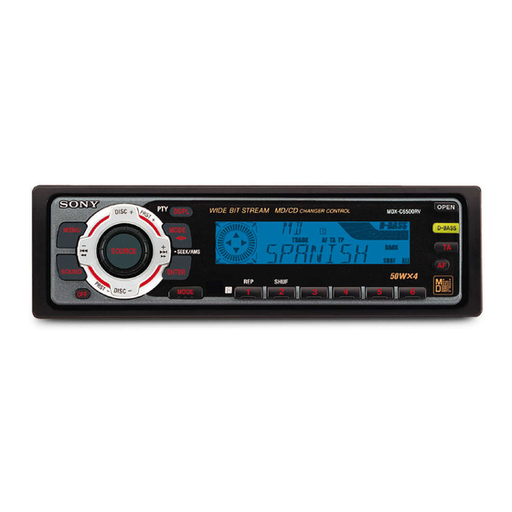
Photo: MDX-C6500R
Model Name Using Similar Mechanism
Base Mechanism Type
Optical Pick-up Name
SPECIFICATIONS
General
90 dB
Outputs
10 – 20,000 Hz
Below measurable limit
Tone controls
87.5 – 108.0 MHz
External aerial connector
Power requirements
10.7 MHz/450 kHz
8 dBf
Dimensions
75 dB at 400 kHz
66 dB (stereo),
Mounting dimensions
72 dB (mono)
Mass
0.6 % (stereo),
Supplied accessories
0.3 % (mono)
35 dB at 1 kHz
30 – 15,000 Hz
1
Equipped with front and rear outputs:
*
MDX-C6500RX/C6500R only
MW: 531 – 1,602 kHz
Equipped with rear outputs: MDX-C6400R
LW: 153 – 279 kHz
2
*
MDX-C6500RX/C6500R only
External aerial connector
10.7 MHz/450 kHz
MW: 30 µV
U.S. and foreign patents licensed from Dolby
LW: 40 µV
laboratories Licensing Corporation.
Design and specifications are subject to change
without notice.
Speaker outputs
(sure seal connectors)
4 – 8 ohms
MDX-C6400R/C6500R/C6500RX
Audio outputs*
1
Power aerial relay control
lead
Power amplifier control
lead
Telephone ATT control
2
lead*
Bass ±9 dB at 100 Hz
Treble ±9 dB at 10 kHz
12 V DC car battery
(negative ground)
Approx. 178 × 50 × 183 mm
(w/h/d)
Approx. 182 × 53 × 162 mm
(w/h/d)
Approx. 1.2 kg
Parts for installation and
connections (1 set)
Front panel case (1)
FM/MW/LW MINIDISC PLAYER
AEP Model
UK Model
MDX-C6500R/C6500RX
NEW
MG-164NZ-138
KMS-241C
Advertisement
Table of Contents

Related Manuals for Sony MDX-C6400R


Summary of Contents for Sony MDX-C6400R
- Page 1 30 – 15,000 Hz Equipped with front and rear outputs: MW/LW MDX-C6500RX/C6500R only Tuning range MW: 531 – 1,602 kHz Equipped with rear outputs: MDX-C6400R LW: 153 – 279 kHz MDX-C6500RX/C6500R only Aerial terminal External aerial connector Intermediate frequency 10.7 MHz/450 kHz MW: 30 µV...
-
Page 2: Table Of Contents
LINE WITH MARK 0 ON THE SCHEMATIC DIAGRAMS AND IN THE PARTS LIST ARE CRITICAL TO SAFE OPERATION. REPLACE THESE COMPONENTS WITH SONY PARTS WHOSE PART NUMBERS APPEAR AS SHOWN IN THIS MANUAL OR IN SUPPLEMENTS PUB- LISHED BY SONY. -
Page 3: General
SECTION 1 This section is extracted from instruction manual. GENERAL Location of controls Setting the clock The clock uses a 24-hour digital indication. Example: To set the clock to 10:08 Press (MENU), then press either side of (DISC/PRST) repeatedly until “CLOCK” OPEN DSPL appears. -
Page 9: Disassembly
SECTION 2 DISASSEMBLY Note: Follow the disassembly procedure in the numerical order given. SUB PANEL ASS’Y 1 screw (PTT2.6 × 5) 2 cover 4 two claws 5 sub panel ass’y 3 screw (PTT2.6 × 8) 4 claw 3 two screws (PTT2.6 ×... - Page 10 SERVO BOARD 2 two screws (BVTT2 × 4) 2 two screws (BVTT2 × 4) 3 servo board 1 sensor flexible board (CN102) 1 flexible board (CN103) MAIN BOARD 1 three ground point screws 2 three screws (PTT2.6 × 10) 3 main board...
- Page 11 MD COVER ASS’Y 1 four screws (B2 × 3) 3 MD cover ass’y shaft (MD cover guide) cassette holder 2 Pushing the Cassette Holder in the direction of the arrow A with a screwdriver, etc., disengage the Shaft (MD Cover Guide) from the slot in the MD Cover Assy.
- Page 12 FLOAT BLOCK 3 Pushing an arrow A part, raise the float block up ward at the front to release a lock. 1 tension spring (FLOAT B) float block lever (lock R) lever (lock L) 1 tension spring (FLOAT B) 2 two tension springs (FLOAT F) LO MOTOR ASS’Y (LOADING) (M903) 4 Remove the bracket (LO) in the direction of the arrow A.
- Page 13 LEVER (LE) ASS’Y 2 stopper washer 2 lever (LE) ass’y 3 roller (GEAR E) HOLDER ASS’Y 4 Remove the holder ass’y in the direction of the arrow. 2 type-E stopring 1.5 1 spring (CHKG) 2 type-E stopring 1.5 2 type-E stopring 1.5 3 lever (lock R) 3 lever (lock L) 1 spring (CHKG)
- Page 14 CHUCKING ARM ASS’Y 1 Remove the chucking arm ass’y in the direction of the arrow. holder ass’y OPTICAL PICK-UP (KMS-241C/J1NP) 4 screw (B2 × 3) 6 bearing (SL) 5 feed screw ass’y 7 optical pick-up (KMS-241C/J1NP) 3 screw (K2 × 3) 1 two screws (K2 ×...
- Page 15 SL MOTOR ASS’Y (SLED) (M902), SP MOTOR ASS’Y (SPINDLE) (M901) 4 screw (P1.7 × 1.8) 9 two screws (P1.7 × 1.8) 5 bracket (SL) 2 two screws (2 × 8) 6 SL motor ass’y (sled) (M902) 0 bracket (SP) 7 screw 3 sensor board (B2 ×...
-
Page 16: Electrical Adjustments
SECTION 3 ELECTRICAL ADJUSTMENTS TEST MODE This set have the test mode function. <Set the Test Mode> 1. Turn ON the regulated power supply. (The clock is displayed) [OFF] Note: Press the button, if the clock is not displayed. 2. Push the preset button. -
Page 17: Diagrams
MDX-C6400R/C6500R/C6500RX SECTION 4 DIAGRAMS IC301 (1/2) 4-1. BLOCK DIAGRAM – SERVO Section – • SIGNAL PATH EFMO ADDT : MD PLAY FILI DIGITAL SIGNAL PROCESSOR, EFM/ACIRC ENCODER/DECODER, SHOCK PROOF MEMORY CONTROLLER, CLTV ATRAC ENCODER/DECODER, 2M BIT D-RAM SAMPLING FILO IC301 (1/2) -
Page 18: Block Diagram - Tuner Section
MDX-C6400R/C6500R/C6500RX 4-2. BLOCK DIAGRAM – TUNER Section – BU B+ TUNER +8.7V TUNER +5.6V FM/AM TUNER UNIT (FM/AM ANTENNA) 2 ANT-FM (Page 19) ANT-AM MUTING Q111 AM-DET (Page 19) 12 13 MUTING Q121 MUTING CONTROL SWITCH Q131 D131 IF-AM (Page 19) -
Page 19: Block Diagram - Main Section
MDX-C6400R/C6500R/C6500RX 4-3. BLOCK DIAGRAM – MAIN Section – CNJ151 (1/2) INPUT SELECT, ELECTRICAL VOLUME, FM MPX AUDIO IN IC151 R-CH DADT, CNJ151 (2/2) BCK, FD1L LOUDNESS/ SOFT TONE LRCK, VOUTL VOLUME MUTE CONTROL FS256 DADT DATA OUTLF (Page 17) MONO... -
Page 20: Block Diagram - Bus Control/Power Supply Section
MDX-C6400R/C6500R/C6500RX 4-4. BLOCK DIAGRAM – BUS CONTROL/POWER SUPPLY Section – REMOTE CONTROL CN701 MASTER CONTROLLER RECEIVER BUS CONTROL IN IC501 (3/3) IC951 (FOR SONY BUS) D708 CN601 (2/2) SIRCS BUFFER SIRCS 24 SIRCS (POWER CONNECTOR) Q704 D673 ANT-R RESET SIGNAL... -
Page 21: Note For Printed Wiring Boards And Schematic Diagrams
MDX-C6400R/C6500R/C6500RX • Circuit Boards Location 4-5. NOTE FOR PRINTED WIRING BOARDS AND SCHEMATIC DIAGRAMS Note on Printed Wiring Board: Note on Schematic Diagram: • X : parts extracted from the component side. • All capacitors are in µF unless otherwise noted. pF: µµF •... -
Page 22: Sensor Board
MDX-C6400R/C6500R/C6500RX 4-6. PRINTED WIRING BOARDS – SERVO Board (Component Side)/SENSOR Board – • See page 21 for Circuit Boards Location. (LOADING END) (COMPONENT SIDE) SERVO BOARD L101 C103 C105 M903 IC401 (LOADING) C109 D401 C403 R406 C108 C352 C306 Q401... -
Page 23: Servo Board (Conductor Side)
MDX-C6400R/C6500R/C6500RX 4-7. PRINTED WIRING BOARD – SERVO Board (Conductor Side) – • See page 21 for Circuit Boards Location. SERVO BOARD (CONDUCTOR SIDE) R402 R401 R104 R403 Q402 B C E R202 C361 Q403 IC307 C307 C358 C301 C356 C511... -
Page 24: Schematic Diagram - Servo Board (1/2)
MDX-C6400R/C6500R/C6500RX 4-8. SCHEMATIC DIAGRAM – SERVO Board (1/2) – • See page 31 for Waveforms. • See page 36 for IC Block Diagrams. • Voltages and waveforms are dc with respect to ground The components identified by mark 0 or dotted under no-signal conditions. -
Page 25: Schematic Diagram - Servo Board (2/2)
MDX-C6400R/C6500R/C6500RX 4-9. SCHEMATIC DIAGRAM – SERVO Board (2/2) – • See page 31 for Waveforms. • See page 36 for IC Block Diagram. (Page • Voltages and waveforms are dc with respect to ground under no-signal conditions. no mark : MD PLAY ∗... -
Page 26: Printed Wiring Board - Main Board (Component Side)
MDX-C6400R/C6500R/C6500RX 4-10. PRINTED WIRING BOARD – MAIN Board (Component Side) – • See page 21 for Circuit Boards Location. • Semiconductor Location Ref. No. Location D301 D501 D502 D551 J-13 D552 K-13 D553 K-13 D554 J-12 D555 K-13 D556 J-12... -
Page 27: Printed Wiring Board - Main Board (Conductor Side)
MDX-C6400R/C6500R/C6500RX 4-11. PRINTED WIRING BOARD – MAIN Board (Conductor Side) – • See page 21 for Circuit Boards Location. (FRONT VIEW) • Semiconductor Location Ref. No. Location H-11 H-11 G-11 D131 F-12 D302 D361 D362 D561 K-11 D562 K-11 D563... -
Page 28: Schematic Diagram - Main Board (1/3)
MDX-C6400R/C6500R/C6500RX 4-12. SCHEMATIC DIAGRAM – MAIN Board (1/3) – • See page 31 for Waveform. • See page 36 for IC Block Diagrams. (Page 30) (Page 29) • Voltages and waveforms are dc with respect to ground under no-signal (detuned) conditions. -
Page 29: Schematic Diagram - Main Board (2/3)
MDX-C6400R/C6500R/C6500RX 4-13. SCHEMATIC DIAGRAM – MAIN Board (2/3) – • See page 31 for Waveforms. (Page 28) (Page (Page • Voltages and waveforms are dc with respect to ground under no-signal (detuned) conditions. no mark : FM ) : MW ] : LW 〈〈... -
Page 30: Schematic Diagram - Main Board (3/3)
MDX-C6400R/C6500R/C6500RX 4-14. SCHEMATIC DIAGRAM – MAIN Board (3/3) – • See page 36 for IC Block Diagrams. (Page (Page (Page • Voltages are dc with respect to ground under no-signal (detuned) conditions. no mark : FM 〈〈 〉〉 : MD PLAY... - Page 31 MDX-C6400R/C6500R/C6500RX • Waveforms – SERVO Board – – MAIN Board – – KEY Board – 1 IC101 1 (XTI) (MD Play Mode) 6 IC301 wh (XBCK) (MD Play Mode) 1 IC51 4 (OSCD) 1 IC901 y; (OSC) qa IC302 1, 2, r;, rh (I, J, AGCI, RFO) (MD Play Mode) 4.4 Vp-p...
-
Page 32: Printed Wiring Board - Sub Board
MDX-C6400R/C6500R/C6500RX 4-15. PRINTED WIRING BOARD – SUB Board – • See page 21 for Circuit Boards Location. (Page 27) (Page 34) -
Page 33: 4-16. Schematic Diagram - Sub Board
MDX-C6400R/C6500R/C6500RX 4-16. SCHEMATIC DIAGRAM – SUB Board – (Page 30) (Page 35) -
Page 34: Printed Wiring Board - Key Board
MDX-C6400R/C6500R/C6500RX 4-17. PRINTED WIRING BOARD – KEY Board – • See page 21 for Circuit Boards Location. • Semiconductor Location Ref. No. Location IC951 LED901 LED902 LED903 LED904 LED910 B-12 LED911 B-12 LED912 A-12 LED913 LED914 LED915 • Semiconductor Location Ref. -
Page 35: Schematic Diagram - Key Board
MDX-C6400R/C6500R/C6500RX 4-18. SCHEMATIC DIAGRAM – KEY Board – • See page 31 for Waveform. (Page • Voltages and waveforms are dc with respect to ground under no-signal (detuned) conditions. no mark : FM... - Page 36 MDX-C6400R/C6500R/C6500RX • IC Block Diagrams IC302 CXA2523AR – SERVO Board – IC101 PCM1718E/2K 43 42 USROP – 20 XTO RF AGC CONTROL – USRC DGND 19 CLKO RFA1 INPUT INTERFACE 18 MUTE BPF3T MODE RFA2 RFA3 CONTROL PEAK3T DIGITAL –...
- Page 37 IC303 BH6511FS-E2 INTERFACE INTERFACE CHARGE PREDRIVE PREDRIVE PUMP. PREDRIVE PREDRIVE INTERFACE INTERFACE IC305 BA6287F OUT1 OUT2 DRIVER DRIVER VREF CONTROL LOGIC POWER SAVE IC307 MN41V4400TT-08S TIMING TIMING GENERATOR GENERATOR WRITE COLUMN CLOCK DECODERS SELECTOR GENERATOR INTERNAL REFRESH SENSE ADDRESS CONTROL AMPLIFIERS COUNTER CLOCK...
-
Page 38: Main Board
– MAIN Board – IC51 SAA6588T/V2-118 POWER SUPPLY PAUSE & RESET DETECTOR MULTI PATH 57kHz DETECTOR 8th ORDER BAND-PASS FILTER CLOCKED SIGNAL QUALITY COMPARATOR DECODER CLOCK CLOCK RDS/RDBS RDS/RDBS INTERFACE DATA DEMODULATOR DECODER REGISTER DATA TEST OSCILLATOR IIC BUS SLAVE &... - Page 39 IC151 TDA7402TR 33 32 31 24 23 MIXER MONO- MONO- MONO- MONO- MONO- MONO- FADER FADER FADER FADER FADER FADER ACINLF FRONT SUBWOOFER SWINR ACIN +PHASE OUTPUT SWINL REAR CONTROL SELECTOR ACOUTR MAIN ACOUTL SECOND CREF VOICE BANDPASS BASS SUPPLY TREBLE HIGH-CUT VOLUME...
-
Page 40: 4-19. Ic Pin Function Description
4-19. IC PIN FUNCTION DESCRIPTION • SERVO BOARD IC301 CXD2652AR (DIGITAL SIGNAL PROCESSOR, DIGITAL SERVO PROCESSOR, EFM/ACIRC ENCODER/DECODER, SHOCK PROOF MEMORY CONTROLLER, ATRAC ENCODER/DECODER, 2M BIT D-RAM) Pin No. Pin Name Description Focus OK signal output to the MD mechanism controller (IC501) MNT0 “H”... - Page 41 Pin No. Pin Name Description Two-way data bus with the D-RAM (IC307) MVCI Digital in PLL oscillation input from the external VCO Not used (fixed at “L”) ASYO Playback EFM full-swing output terminal ASYI I (A) Playback EFM asymmetry comparator voltage input terminal AVDD —...
- Page 42 Pin No. Pin Name Description FRDR Focus servo drive PWM signal (–) output to the BH6511FS (IC303) Clock signal (176.4 kHz) output terminal (X’tal system) Not used (open) SRDR Sled servo drive PWM signal (–) output to the BH6511FS (IC303) SFDR Sled servo drive PWM signal (+) output to the BH6511FS (IC303) SPRD...
- Page 43 • SERVO BOARD IC302 CXA2523AR (RF AMP, FOCUS/TRACKING ERROR AMP) Pin No. Pin Name Description I-V converted RF signal I input from the optical pick-up block detector I-V converted RF signal J input from the optical pick-up block detector Middle point voltage (+1.65V) generation output terminal 4 to 9 A to F Signal input from the optical pick-up detector...
- Page 44 Two way data bus with the external EEPROM device Not used (open) MD-SO Writing serial data signal output to the CXD2652AR (IC301) and CXA2523AR (IC302) LINKOFF Unilink on/off control signal output for the SONY bus “L”: link on, “H”: link off...
- Page 45 Pin Name Description UNIREQ Data request signal output terminal (for SONY bus) “H”: request on Not used (open) Serial clock signal input from the master controller (IC501) or serial clock signal output to the UNICKIO SONY bus interface (IC701) and master controller (IC501) (for SONY bus)
- Page 46 Tuner system power supply on/off control signal output terminal “H”: tuner power on ANT CUT Not used (open) Bus on/off control signal output to the MD mechanism controller (IC501) and SONY bus BUSON interface (IC701) “L”: bus on 4 to 6...
- Page 47 Input of acknowledge signal for the key entry Acknowledge signal is input to accept function KEYACK and eject keys in the power off status On at input of “H” Battery detection signal input from the SONY bus interface (IC701) and battery detect circuit BUIN “L” is input at low voltage...
- Page 48 “H” is input at dimmer detection Not used (fixed at “L”) Telephone detection signal input terminal At input of “H”, the signal is attenuated by –20 dB TELATT Used for the MDX-C6500R/C6500RX only (MDX-C6400R: fixed at “L”) Not used (open) TEST IN Setting terminal for the test mode “L”: test mode, Normally: fixed at “H”...
- Page 49 Pin No. Pin Name Description Dolby control in/out terminal At initial mode: valid/invalid selection input of dolby function (valid at “L” input) DOLON At normal mode: dolby on/off control signal output terminal (dolby on at “H” output) Not used this function (open) TAPATT Audio signal select control signal output terminal Not used (open) Not used (open)
-
Page 50: Exploded Views
Ver 1.2 SECTION 5 EXPLODED VIEWS NOTE: • Items marked “*” are not stocked since they • -XX and -X mean standardized parts, so they The components identified by mark 0 or dotted line with mark may have some difference from the original are seldom required for routine service. - Page 51 (2) FRONT PANEL SECTION not supplied (KEY board) LCD901 Ref. No. Part No. Description Remark Ref. No. Part No. Description Remark 3-041-010-01 BUTTON (1-6/M) (MODE. 1. 2. 3. 4. 5. 6) X-3378-398-1 PANEL ASSY, FRONT BACK 3-040-987-01 BUTTON (OFF) 3-935-151-01 SPRING (OPEN) 3-040-986-01 BUTTON (MENU/SOUND) 3-040-989-01 BUTTON (OPEN) 3-041-003-01 BUTTON (LIST/ENTER) (DSPL.
- Page 52 (3) MECHANISM DECK SECTION-1 (MG-164NZ-138) Ref. No. Part No. Description Remark Ref. No. Part No. Description Remark * 101 A-3326-036-A SERVO BOARD, COMPLETE * 110 3-032-712-01 LEVER (LOCK R) * 102 X-3376-799-1 CHASSIS ASSY, MD 3-919-281-01 SPRING (CHUCKING) 3-032-714-02 SPRING (FLOAT F), TENSION * 112 X-3376-800-1 COVER ASSY, MD 3-921-111-01 SPRING (FLOAT B), TENSION...
- Page 53 (4) MECHANISM DECK SECTION-2 (MG-164NZ-138) M903 M901 M902 The components identified by mark 0 or dotted line with mark 0 are critical for safety. Replace only with part number specified. Ref. No. Part No. Description Remark Ref. No. Part No. Description Remark 2-626-617-01 SCREW (2X8)
-
Page 54: Electrical Parts List
SECTION 6 ELECTRICAL PARTS LIST NOTE: • Due to standardization, replacements in the • Items marked “*” are not stocked since they The components identified by mark 0 or dotted line with mark parts list may be different from the parts speci- are seldom required for routine service. - Page 55 Ref. No. Part No. Description Remark Ref. No. Part No. Description Remark R909 1-216-667-11 METAL CHIP 4.7K 0.5% 1/10W LSW906 1-762-617-21 SWITCH, KEY BOARD (WITH LED) (LIST) R910 1-216-671-11 METAL CHIP 6.8K 0.5% 1/10W (AMBER) LSW906 1-762-619-21 SWITCH, KEY BOARD (WITH LED) (LIST) R911 1-208-806-11 RES, CHIP 1/10W...
- Page 56 MAIN Ref. No. Part No. Description Remark Ref. No. Part No. Description Remark R976 1-216-815-11 METAL CHIP 1/16W 1-163-809-11 CERAMIC CHIP 0.047uF R977 1-216-815-11 METAL CHIP 1/16W 1-164-004-11 CERAMIC CHIP 0.1uF R980 1-216-864-11 METAL CHIP 1/16W 1-164-004-11 CERAMIC CHIP 0.1uF C101 1-126-160-11 ELECT R999...
- Page 57 MAIN Ref. No. Part No. Description Remark Ref. No. Part No. Description Remark C502 1-164-004-11 CERAMIC CHIP 0.1uF < DIODE > C503 1-164-004-11 CERAMIC CHIP 0.1uF C504 1-164-004-11 CERAMIC CHIP 0.1uF 8-719-073-01 DIODE MA111-TX C505 1-164-004-11 CERAMIC CHIP 0.1uF 8-719-067-56 DIODE MA112-TX 8-719-073-01 DIODE MA111-TX C506 1-163-235-11 CERAMIC CHIP...
- Page 58 MAIN Ref. No. Part No. Description Remark Ref. No. Part No. Description Remark D703 8-719-056-82 DIODE UDZ-TE-17-6.2B Q121 8-729-920-21 TRANSISTOR DTC314TK-T-146 Q131 8-729-921-25 TRANSISTOR FMC2-T148 D704 8-719-056-93 DIODE UDZ-TE-17-18B D705 8-719-056-93 DIODE UDZ-TE-17-18B Q171 8-729-920-21 TRANSISTOR DTC314TK-T-146 D706 8-719-072-70 DIODE MA2ZD14001S0 Q181 8-729-920-21 TRANSISTOR DTC314TK-T-146 D708...
- Page 59 MAIN Ref. No. Part No. Description Remark Ref. No. Part No. Description Remark R131 1-216-037-00 METAL CHIP 1/10W R551 1-249-413-11 CARBON 1/4W R132 1-216-045-00 METAL CHIP 1/10W (C6500RX) R141 1-216-025-00 RES, CHIP 1/10W R142 1-216-073-00 METAL CHIP 1/10W R552 1-216-025-00 RES, CHIP 1/10W R553 1-216-025-00 RES, CHIP...
- Page 60 Ver 1.2 MAIN SENSOR SERVO Ref. No. Part No. Description Remark Ref. No. Part No. Description Remark < SWITCH > C325 1-110-563-11 CERAMIC CHIP 0.068uF C326 1-162-968-11 CERAMIC CHIP 0.0047uF 10% SW503 1-692-431-21 SWITCH, TACTILE (RESET) C327 1-109-982-11 CERAMIC CHIP SW504 1-771-540-11 SWITCH, PUSH (1KEY) (NOSE DETECT) C328 1-162-966-11 CERAMIC CHIP...
- Page 61 SERVO Ref. No. Part No. Description Remark Ref. No. Part No. Description Remark < FERRITE BEAD > R324 1-216-827-11 METAL CHIP 3.3K 1/16W R325 1-216-821-11 METAL CHIP 1/16W FB301 1-414-235-22 FERRITE BEAD INDUCTOR CHIP R327 1-216-821-11 METAL CHIP 1/16W FB302 1-414-760-21 FERRITE BEAD INDUCTOR CHIP R328 1-216-811-11 METAL CHIP...
- Page 62 SERVO Ref. No. Part No. Description Remark Ref. No. Part No. Description Remark R524 1-216-821-11 METAL CHIP 1/16W MISCELLANEOUS R525 1-216-845-11 METAL CHIP 100K 1/16W ************** R526 1-216-825-11 METAL CHIP 2.2K 1/16W 1-776-527-51 CORD (WITH CONNECTOR) (ISO) (POWER) R527 1-216-825-11 METAL CHIP 2.2K 1/16W (C6400R)
- Page 63 Ver 1.1 2001.05 Ref. No. Part No. Description Remark Ref. No. Part No. Description Remark PARTS FOR INSTALLATION AND CONNECTION ************************************* 1-465-459-21 ADAPTER, ANTENNA 3-012-360-31 FRAME 3-040-979-01 COLLAR 3-233-644-01 SPRING, FITTING 3-934-325-01 SCREW, +K (5X8) TAPPING X-3366-405-1 SCREW ASSY (EXP), FITTING 1-776-527-51 CORD (WITH CONNECTOR) (ISO) (POWER) (C6400R) 1-776-527-61 CORD (WITH CONNECTOR) (ISO) (POWER)
- Page 64 MDX-C6400R/C6500R/C6500RX REVISION HISTORY Clicking the version allows you to jump to the revised page. Also, clicking the version at the upper right on the revised page allows you to jump to the next revised page. Ver. Date Description of Revision 2001.12...