Harman Kardon AVR347 Service Manual
7 x 55w 7.1 channel a/v receiver
Hide thumbs
Also See for AVR347:
- Owner's manual (76 pages) ,
- Worksheet (3 pages) ,
- Reference manual (1 page)
Table of Contents
Advertisement
harman/kardon
7 X 55W 7.1 CHANNEL A/V RECEIVER
ESD WARNING.....................................2
LEAKAGE TESTING...............................3
BASIC SPECIFICATIONS.......................4
PACKAGING........................................5
FRONT PANEL CONTROLS.....................6
REAR PANEL CONNECTIONS................8
REMOTE CONTROL FUNCTIONS..........11
CONNECTIONS..................................14
OPERATION.......................................33
TROUBLESHOOTING GUIDE.................41
PROCESSOR RESET............................42
AVR347
SERVICE MANUAL
CONTENTS
harman/kardon, Inc.
250 Crossways Park Dr.
Woodbury, New York 11797
DISASSEMBLY....................................43
UNIT EXPLODED VIEW..........................48
EXPLODED VIEW PARTS LIST...............49
AMP BIAS ADJUSTMENT......................50
BLOCK DIAGRAM................................51
ELECTRICAL PARTS LIST....................52
PCB DRAWINGS.................................98
SEMICONDUCTOR PINOUTS...............107
SCHEMATICS....................................209
WIRING DIAGRAM...................................219
Rev 0
6/2007
Advertisement
Table of Contents

Related Manuals for Harman Kardon AVR347


Summary of Contents for Harman Kardon AVR347
-
Page 1: Table Of Contents
AVR347 7 X 55W 7.1 CHANNEL A/V RECEIVER SERVICE MANUAL CONTENTS ESD WARNING……………………………….2 DISASSEMBLY………………………………43 LEAKAGE TESTING……………….…..…..3 UNIT EXPLODED VIEW……………………..48 BASIC SPECIFICATIONS…………………..4 EXPLODED VIEW PARTS LIST……………49 PACKAGING………………………..………..5 AMP BIAS ADJUSTMENT………………….50 FRONT PANEL CONTROLS………..…..…..6 BLOCK DIAGRAM…………………………..51 REAR PANEL CONNECTIONS………….…8 ELECTRICAL PARTS LIST……………..…52 REMOTE CONTROL FUNCTIONS.………11... -
Page 2: Esd Warning
AVR347 Some semiconductor (solid state) devices can be damaged easily by static electricity. Such components commonly are called Electrostatically Sensitive (ES) Devices. Examples of typical ES devices are integrated circuits and some field effect transistors and semiconductor "chip" components. -
Page 3: Leakage Testing
AVR347 SAFETY PRECAUTIONS The following check should be performed for the continued protection of the customer and service technician. LEAKAGE CURRENT CHECK Measure leakage current to a known earth ground (water pipe, conduit, etc.) by connecting a leakage current tester... -
Page 4: Basic Specifications
All features and specifications are subject to change without notice. Distortion (TIM) Unmeasurable Slew Rate 40V/µsec Harman Kardon and Logic 7 are trademarks of Harman International Industries, Incorporated, registered in the United States and/or other countries. EzSet/EQ, and Designed to Entertain are trademarks Bridge of Harman International Industries, Incorporated. -
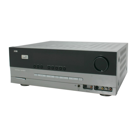
Page 6: Front Panel Controls
AVR347 FRONT-PANEL CONTROLS Main Power Switch: Surround Mode: This mechanical switch turns the power supply Press this button to select a surround sound (e.g., on or off. It is usually left pressed in (On position), and cannot be turned multichannel) mode group. - Page 7 AVR347 Source Digital Input Message Display Speaker Size Indicators Select Tone Mode Setup Speaker/Channel Channel Level Surround Mode Indicators Delay Volume Navigation Input Indicators Adjust Headphone Jack/EzSet/EQ Power Surround Tuning Preset Stations Digital Video 4 Microphone Indicator Mode Audio Inputs...
-
Page 8: Rear Panel Connections
AVR347 REAR-PANEL CONNECTIONS AM and FM Antenna Terminals: Remote IR Carrier Output: Connect the included AM and This output is similar in function to FM antennas to their respective terminals for radio reception. the Remote IR Output, with the difference that this jack outputs the full infrared signal as received by the AVR’s IR sensor or the Remote... - Page 9 This specialized connector may be used with a compatible digital audio output, connect it to one of these jacks your personal computer in case Harman Kardon offers a software for improved audio performance. Use only one type of digital audio upgrade for the receiver at some time in the future.
- Page 10 AVR347 Component Coaxial Digital Video Video 3 Audio Video 1 RS-232 DVD A/V Inputs Antenna Inputs RS-232 Tape Serial Port Inputs Inputs (1, 2 & 3) Jack (1, 2 & 3) FM Antenna Reset Outputs Outputs Component HDMI 2...
-
Page 11: Remote Control Functions
AVR347 MAIN REMOTE CONTROL FUNCTIONS The AVR 347 remote is capable of controlling 11 devices, including the IR Transmitter Lens: As buttons are pressed on the remote, AVR itself and an iPod docked in the optional The Bridge accessory. - Page 12 AVR347 IR Transmitter Lens Power On Mute Program Indicator Power Off AVR Selector Input Selectors AM/FM 6-/8-Channel Input Selector Learn XM Radio Test Tone TV/Video Sleep Volume Controls DSP Surround Multiroom On-Screen Display Speaker Setup Channel Level Navigation Digital Input...
-
Page 13: Main Remote Control Functions
AVR347 MAIN REMOTE CONTROL FUNCTIONS On-Screen Display (OSD): press the Set Button repeatedly until PRESET SEARCH appears. Use Press this button to activate the Buttons to select a letter (A through E) representing one of on-screen menu system. ⁄... -
Page 14: Connections
Composite harman/kardon S-Video AVR347 CONNECTIONS There are different types of audio and video connections used to Bare wire cables are installed as follows (see Figure 2): connect the receiver to the speakers and video display, and to connect 1. Unscrew the terminal cap until the pass-through hole in the collar is the source devices to the receiver. -
Page 15: Audio Connections
Whichever type of connection Digital Audio Connections you choose, Harman Kardon recommends that you always select the Coaxial highest quality cables available within your budget. - Page 16 Both the chrominance (color) and Audio Connections luminance (intensity) components of the video signal are transmitted Harman Kardon receivers also include a proprietary, dedicated audio Left Right using a single cable. See Figure 10.
- Page 17 The RS-232 serial port on the AVR 347 is used only for data. If Left Right Component Harman Kardon releases a software upgrade for the receiver’s operating Front (FL/FR) video cable Center (C) system at some time in the future, the upgrade may be downloaded Surround (SL/SR) to the AVR using this port.
- Page 18 AVR347 INSTALLATION You are now ready to connect your various components to your receiver. Step Three – Connect the Antennas Before beginning, make sure that all components, including the AVR 347, Connect the FM and AM antennas to their terminals. If you have purchased are turned completely off and their power cords are unplugged.
- Page 19 AVR347 INSTALLATION For each video source, select one type of video connection. HDMI video NOTE: It’s possible for a source to use none of the connections is preferred, but both your source device and your video display must named for that source. For example, you might connect your have this type of video capability.
- Page 20 AVR347 INSTALLATION NOTE: The AVR 347 is equipped with a total of eight digital audio inputs, not including the HDMI inputs: six on the rear panel (Coaxial 1, 2 and 3, Optical 1, 2 and 3) and two on the front panel (Coaxial 4 and Optical 4).
- Page 21 Bridge Make sure your video display is HDMI-capable, and for many source With Harman Kardon’s optional The Bridge, you can listen to audio or devices, the display must be HDCP-compliant (High-Bandwidth Digital view videos stored on your iPod (not included), use your AVR 347...
- Page 22 AVR347 INSTALLATION remote control to operate the iPod, and even charge the iPod while If you used component video for any sources, connect the Component it’s docked in The Bridge. Video Monitor Outputs on the receiver to one set of component video inputs on your display.
- Page 23 The AVR 347’s remote is factory-programmed to control an iPod docked in The Bridge and many Harman Kardon DVD and CD players. If you have other source devices in your system, follow these steps to program the correct codes into the remote.
- Page 24 Control Code and operate it using the device’s original remote control. Alternatively, Video 1 VCR, PVR you may wish to consider purchasing Harman Kardon’s optional TC 30 Video 2 Cable, Satellite activity-based remote, which is programmed by accessing a large data- Video 3 base of product codes on the Internet.
- Page 25 See Figure 40. away from the listener, you may connect an external IR receiver, such as the optional Harman Kardon HE 1000, to the Remote IR Input jack. When you are using the AVR 347 in multiroom mode, you may connect...
- Page 26 AVR347 INSTALLATION 3. Connect an external amplifier to the Surround Back/Multiroom Preamp Outputs. See Figure 42. Figure 42 – Surround Back/Multiroom Preamp Outputs Figure 44 – Power Switches This method may be used when it is more important to distribute 2.
-
Page 27: Initial Setup
AVR347 INITIAL SETUP Before you begin enjoying your new receiver, a few adjustments should be made to configure the AVR 347 to match your actual system. Make sure that you have connected a video display to one of the video monitor outputs on the receiver. - Page 28 AVR347 INITIAL SETUP The Initial Setup section requires that you complete all of the steps in the Installation section that apply to your receiver. You should have connected all of your loudspeakers and a video display, as well as your source devices.
- Page 29 AVR347 INITIAL SETUP surround back speaker to the left Surround Back Speaker Output, and then configure the surround back speaker manually, as described in the Advanced Functions section. However, we do not recommend the 6.1-channel configuration. If you have forgotten to plug in the EzSet/EQ microphone, the warning screen shown in Figure 55 will appear as a reminder.
-
Page 30: Configure Sources
AVR347 INITIAL SETUP display device or set-top box causes delays while digital video is making these adjustments a screen similar to the one shown in signals are processed. It simultaneously adds a delay to all Figure 59 will appear. You may hear EzSet/EQ repeat tones from various speaker channels in the system. - Page 31 AVR347 INITIAL SETUP The first line indicates that the receiver is currently set to the DVD source. NOTES: • Only upper case letters are available for titles. Press the Set Button, and then use the › to view the next source.
- Page 32 AVR347 INITIAL SETUP AUDIO IN: By default, the analog audio inputs are assigned at the factory to all sources, with the following exceptions: Table 6 – Default Digital Audio Assignments Source Input Default Digital Audio Input Coax 1 Video 2...
-
Page 33: Operation
AVR347 OPERATION Now that you have installed your system components and completed at settings you have programmed, including system configuration and least a basic configuration of your receiver, you are ready to begin preset radio stations, will be preserved for up to four weeks. -
Page 34: Mute Function
AVR347 OPERATION Mute Function NOTE: The AVR 347 does not have a conventional balance control. The EzSet/EQ process compensates for any character- To temporarily mute all speakers and the headphones, press the Mute istics of your room or speakers, and we recommend that you Button on the remote. -
Page 35: Audio Input Selection
AVR347 OPERATION of any of these three Input Selectors will select the source whose name If your iPod is capable of playing still images and videos, it may be used appears on the button (i.e., DVD, Tape or HDMI 1), as indicated by the as a video source. -
Page 36: Using The Tuner
AVR347 OPERATION 6-/8-Channel Direct Inputs audio found on a DVD-Video disc) and video via the HDMI connection. It is not necessary to make a separate digital audio connection. If you wish to hear audio through the 6-/8-Channel Direct Inputs together b) Connect the player’s 6-channel analog audio outputs to the AVR’s... -
Page 37: Xm Radio Operation
AVR347 OPERATION XM service when an optional XM antenna module is connected and the service activated. As of this writing, the Audiovox ® CNP 1000 “Connect and Play” module for home audio use and the XM Mini-Tuner and Home Dock (Models CNP-2000 and CNP-2000H) are compatible with Figure 74 –... - Page 38 AVR347 OPERATION Tune to Channel 0 for a display of your antenna module’s Radio ID Bridge Using number, required for activation. The Bridge is an optional dock that may be used with a compatible iPod The current channel number and preset location will appear in the upper (not included).
- Page 39 AVR347 OPERATION Table 7 summarizes the controls available when The Bridge is in use. See also Figures 82 and 83. Table 7 – Using The Bridge iPod Function Remote Control Key Front-Panel Button Play Play ( › Tuner Mode...
-
Page 40: Selecting A Surround Mode
AVR347 OPERATION NOTES ON VIDEO PLAYBACK: Surround Setup menu, as shown in Figure 86. With the Surround Mode highlighted, press the Set Button to change the surround mode group. • Before attempting to play videos stored on your iPod, check ‹... -
Page 41: Troubleshooting Guide
• Amplifier is in protection mode • Contact your local Harman Kardon service center due to internal problems No sound from surround or • Incorrect surround mode • Select a mode other than Stereo center speakers •... -
Page 42: Processor Reset
AVR347 Erasing Macros It isn’t possible to “edit” a command within a macro. However, you may erase the macro as follows: • Simultaneously press and hold the Mute Button and the Macro Button containing the macro until the LED flashes. -
Page 43: Disassembly
AVR347 DISASSEMBLY AVR347 1. Removing the Top Cabinet 3. Removing the Rear Panel Remove the Screws Remove the Screws 20 21 25 26 32 33 4. Removing the Main PCB Remove the Screws 2. Removing the Front Panel Remove the Screws... - Page 44 AVR347 AVR347 DISASSEMBLY PROCEDURE 1 TOP-CABINET (21) REMOVAL 1. Remove 13 screws (S1,S7) and then remove the Top-cabinet. 2 FRONT PANEL ASS’Y REMOVAL 1. Remove the Top-cabinet, referring to the previous step 1. 2. Disconnect the card cable between connector (CN72-17p) on the Fip PCB (37-1) and connector (CN72) on the Input PCB (39-1).
- Page 45 AVR347 6. Disconnect the connector (CN89) on the Fip PCB (37-1) from lead wire (BN89-4P) on the Key PCB (37-2). 7. Remove 3 screws (S2) and then remove the Guide PCB (37-8) & the Fip PCB (37-1). 7 KEY PCB (37-2) REMOVAL 1.
- Page 46 AVR347 4. Disconnect the card cable between connector (BN21-7P) on XM PCB (39-4) and connector (CN21) on the input PCB (39-1). 5. Disconnect the lead wire (BN85-2P) on the XM PCB (39-4) from connector (CN85) on the Regulator PCB (A)(40-2).
- Page 47 AVR347 3. Disconnect the card cable between connector (CN16-12P) on Input PCB (39-1) and connector (BN16-12P) on A-BUS PCB (39-3). 4. Remove 3screws (S13) and then remove the A-BUS PCB ASS’Y (39-3). 18 MAIN PCB ASS’Y (38-1) REMOVAL 1. Remove the Top-cabinet, referring to the previous step 1.
-
Page 48: Unit Exploded View
AVR347 AVR 347 EXPLODED VIEW 37-7 40-3 40-1 39-2 40-4 39-4 39-1 40-5 39-6 39-3 38-2 38-1 40-7 40-2 DESCRIPTION PARTS NO. Q,ty REMARK ORNAMENT,VOLUME CGU1A318Z CAP,VOLUME CGX1A338MBC63 HOLDER,VOLUME CMH1A214 INDICATOR,VOLUME CGL1A222 WINDOW ASS'Y CGUAVR347 WINDOW,FIP CGU1A399Y BADGE,MODEL CGB1A180Z... -
Page 49: Exploded View Parts List
AVR347... -
Page 50: Amp Bias Adjustment
AVR347... - Page 51 AVR347...
-
Page 52: Electrical Parts List
AVR347 AVR347 Electrical Parts List Ref. Designator Part Number Description FRONT PCB ASSY (CUP11910-1) Capacitors C714 HCBS1H151KBT CAP , CERAMIC 150UF 50V K C716 CCEA1AH331T CAP , ELECT 330UF 10V C723 HCBS1H104ZFT CAP , CERAMIC 0.1UF 50V Z C728... - Page 53 AVR347 Ref. Designator Part Number Description FRONT PCB ASSY (CUP11910-1) R893 CRD20TJ333T RES , CARBON 33K OHM 1/5W J R895 CRD20TJ101T RES , CARBON 100 OHM 1/5W J R920 CRD20TJ102T RES , CARBON 1K OHM 1/5W J Miscellaneous FIP1 HFLHCA18ML03 F.I.P...
- Page 54 AVR347 Ref. Designator Part Number Description PCB , FRONT PANEL KEY (CUP11818-2) Resistors R753 CRD20TF1001T RES , CARBON 1K /1/5W /F R754 CRD20TF1501T RES , CARBON 1.5K /1/5W /F R755 CRD20TF1801T RES , CARBON 1.8K /1/5W /F R756 CRD20TF2701T RES , CARBON 2.7K /1/5W/F...
- Page 55 AVR347 Ref. Designator Part Number Description PCB , HEADPHONE (CUP11910-5) C872 CCEA1CH331T CAP , ELECT 330UF 16V C873 CCEA1CH331T CAP , ELECT 330UF 16V C889 HCBS1H104ZFT CAP , CERAMIC 0.1UF 50V Z Semiconductors D784 CVD1SS133MT DIODE 1SS133 D785 CVD1SS133MT...
- Page 56 AVR347 Ref. Designator Part Number Description PCB , DIGITAL INPUT (CUP11916-1) BN17 KJP12GB143ZP DIP SOCKET DIP SOCKET C750 CCEA1CH101T CAP , ELECT 100UF 16V C751 CCEA1CH101T CAP , ELECT 100UF 16V C752 CCEA1CH101T CAP , ELECT 100UF 16V C753...
- Page 57 AVR347 Ref. Designator Part Number Description PCB , VOLUME ENCODER (CUP11910-6) D703 CVD52CSBBCEAB2 BLUE L.E.D L.E.D D705 CVD52CSBBCEAB2 BLUE L.E.D L.E.D D774 CVD1SS133MT DIODE 1SS133 Resistors J906 CRD20TJ391T RES , CARBON 390OHM 1/5W R402 CRD20TJ101T RES , CARBON 100 OHM 1/5W J...
- Page 58 AVR347 Ref. Designator Part Number Description INPUT PCB (CUP11913-1) C212 CCUS1H221JA CAP , CHIP 220PF C213 CCUS1H221JA CAP , CHIP 220PF C214 CCUS1H221JA CAP , CHIP 220PF C215 CCUS1H221JA CAP , CHIP 220PF C216 CCUS1H221JA CAP , CHIP 220PF...
- Page 59 AVR347 Ref. Designator Part Number Description INPUT PCB (CUP11913-1) C335 CCUS1H681JA CAP , CHIP 680PF C336 CCUS1H681JA CAP , CHIP 680PF C337 CCUS1H223KC CAP , CHIP 0.022UF C338 CCUS1H223KC CAP , CHIP 0.022UF C339 CCUS1H223KC CAP , CHIP 0.022UF...
- Page 60 AVR347 Ref. Designator Part Number Description INPUT PCB (CUP11913-1) C705 CCUS1H104KC CAP , CHIP 0.1UF C707 CCUS1H102KC CAP , CHIP 1000PF C708 CCUS1H104KC CAP , CHIP 0.1UF C716 CCUS1H151JA CAP , CHIP 150PF C718 CCUS1H104KC CAP , CHIP 0.1UF...
- Page 61 AVR347 Ref. Designator Part Number Description INPUT PCB (CUP11913-1) C263 CCEA1EH470T CAP , ELECT 47UF 25V C264 CCEA1EH470T CAP , ELECT 47UF 25V C265 CCEA1EH470T CAP , ELECT 47UF 25V C266 CCEA1EH470T CAP , ELECT 47UF 25V C267 CCEA1EH470T...
- Page 62 AVR347 Ref. Designator Part Number Description INPUT PCB (CUP11913-1) C703 CCEA1CH101T CAP , ELECT 100UF 16V C706 CCEA1CH101T CAP , ELECT 100UF 16V C715 CCEA1HH4R7T CAP , ELECT 4.7UF 50V C717 CCEA1HH4R7T CAP , ELECT 4.7UF 50V C720 CCEA1CH101T...
- Page 63 AVR347 Ref. Designator Part Number Description INPUT PCB (CUP11913-1) IC50 HVINJM2068MDTE1 I.C , DUAL OP AMP IC70 HVITC74VHC157FT I.C, 2-CHANNEL MUX IC71 HVITC74VHC157FT I.C, 2-CHANNEL MUX IC72 HVI74HCU04AFNG I.C , HEX INVERTER TOSHIBA IC73 HVICS42528-CQ I.C , CODEC + DIR...
- Page 64 AVR347 Ref. Designator Part Number Description INPUT PCB (CUP11913-1) RN75 CRJ104DJ330T RES , 4ARRAY (1608*4) 33 OHM/1608*4 RN76 CRJ104DJ330T RES , 4ARRAY (1608*4) 33 OHM/1608*4 RN77 CRJ104DJ330T RES , 4ARRAY (1608*4) 33 OHM/1608*4 RN78 CRJ104DJ330T RES , 4ARRAY (1608*4)
- Page 65 AVR347 Ref. Designator Part Number Description INPUT PCB (CUP11913-1) R248 CRJ10DJ474T RES , CHIP 470K OHM R249 CRJ10DJ474T RES , CHIP 470K OHM R250 CRJ10DJ103T RES , CHIP 10K OHM R251 CRJ10DJ474T RES , CHIP 470K OHM R252 CRJ10DJ474T...
- Page 66 AVR347 Ref. Designator Part Number Description INPUT PCB (CUP11913-1) R313 CRJ10DJ272T RES , CHIP 2.7K OHM R314 CRJ10DJ272T RES , CHIP 2.7K OHM R315 CRJ10DJ272T RES , CHIP 2.7K OHM R316 CRJ10DJ272T RES , CHIP 2.7K OHM R317 CRJ10DJ561T...
- Page 67 AVR347 Ref. Designator Part Number Description INPUT PCB (CUP11913-1) R396 CRJ10DF3920T RES. CHIP (392R 1%) 392 OHM R397 CRJ10DF3920T RES. CHIP (392R 1%) 392 OHM R398 CRJ10DF3920T RES. CHIP (392R 1%) 392 OHM R531 CRJ10DJ152T RES , CHIP 1.5K OHM...
- Page 68 AVR347 Ref. Designator Part Number Description INPUT PCB (CUP11913-1) R777 CRJ10DJ102T RES , CHIP 1K OHM R778 CRJ10DJ103T RES , CHIP 10K OHM R779 CRJ10DJ103T RES , CHIP 10K OHM R780 CRJ10DJ103T RES , CHIP 10K OHM R781 CRJ10DJ103T...
- Page 69 AVR347 Ref. Designator Part Number Description INPUT PCB (CUP11913-1) L705 HLZ9R005Z BEAD CHIP 60(1608 SIZE) HH-1M1608-600 MAIN PCB (CUP11911) Capacitors C501 CCEA1HH100T CAP , ELECT 10UF 50V C502 CCEA1HH100T CAP , ELECT 10UF 50V C503 CCEA1HH100T CAP , ELECT...
- Page 70 AVR347 Ref. Designator Part Number Description MAIN PCB (CUP11911) C812 CCEA1CH101T CAP , ELECT 100UF 16V C813 CCEA1CH101T CAP , ELECT 100UF 16V C814 CCEA1CH101T CAP , ELECT 100UF 16V C815 CCKT1H331KB CAP , CERAMIC 330PF 50V C816 HCBS1H331KBT...
- Page 71 AVR347 Ref. Designator Part Number Description MAIN PCB (CUP11911) C902 CCET63VKL5822NK CAP , ELECT 8200UF 63V C904 KCKDKS472ME CAP , CERAMIC(X1/Y2/SC) 0.0047UF 2.5KV C906 CCEA1EH102E CAP , ELECT 1000UF 25V C909 CCET63VKL5822NK CAP , ELECT 8200UF 63V C911 CCEA1EH471T...
- Page 72 AVR347 Ref. Designator Part Number Description MAIN PCB (CUP11911) Q519 HVTKTC3200GRT KTC3200GR TRANSISTOR NPN Q520 HVTKTC3200GRT TRANSISTOR NPN KTC3200GR Q541 HVTKTC3198YT KTC3198Y TRANSISTOR NPN Q542 HVTKTC3198YT TRANSISTOR NPN KTC3198Y Q543 HVTKTC3198YT TRANSISTOR NPN KTC3198Y Q544 HVTKTC3198YT TRANSISTOR NPN KTC3198Y...
- Page 73 AVR347 Ref. Designator Part Number Description MAIN PCB (CUP11911) Q992 HVTKRA107MT KRA107M TRANSISTOR PNP Q993 HVTKRA107MT TRANSISTOR PNP KRA107M Q994 HVTKRC107MT KRC107M TRANSISTOR NPN Q997 HVTKRA107MT TRANSISTOR PNP KRA107M Q998 HVTKRC107MT TRANSISTOR NPN KRC107M IC94 HVIMC7805C I.C, REGULATOR(+5V) FAIRCHILD...
- Page 74 AVR347 Ref. Designator Part Number Description MAIN PCB (CUP11911) R543 CRD20TJ271T RES , CARBON 270 OHM 1/5W J R544 CRD20TJ271T RES , CARBON 270 OHM 1/5W J R545 CRD20TJ271T RES , CARBON 270 OHM 1/5W J R556 CRD20TJ273T RES , CARBON...
- Page 75 AVR347 Ref. Designator Part Number Description MAIN PCB (CUP11911) R632 CRD25FJ180T RES , CARBON 18 OHM 1/4W R633 CRD25FJ180T RES , CARBON 18 OHM 1/4W R634 CRD25FJ180T RES , CARBON 18 OHM 1/4W R635 CRD25FJ180T RES , CARBON 18 OHM 1/4W...
- Page 76 AVR347 Ref. Designator Part Number Description MAIN PCB (CUP11911) R775 CRD20TJ750T RES , CARBON 75 OHM 1/5W J R776 CRD20TJ750T RES , CARBON 75 OHM 1/5W J R777 CRD20TJ750T RES , CARBON 75 OHM 1/5W J R781 CRD20TJ750T RES , CARBON...
- Page 77 AVR347 Ref. Designator Part Number Description MAIN PCB (CUP11911) R863 CRD20TJ333T RES , CARBON 33K OHM 1/5W J R870 CRD20TJ433T RES , CARBON 43K OHM 1/5W J R871 CRD20TJ433T RES , CARBON 43K OHM 1/5W J R872 CRD20TJ471T RES , CARBON...
- Page 78 AVR347 Ref. Designator Part Number Description MAIN PCB (CUP11911) R968 CRD20TJ105T RES , CARBON 1M OHM 1/5W J R969 CRD20TJ103T RES , CARBON 10K OHM 1/5W J R980 CRD20TJ473T RES , CARBON 47K OHM 1/5W J R986 CRD20TJ102T RES , CARBON...
- Page 79 AVR347 Ref. Designator Part Number Description MAIN PCB (CUP11911) JK91 CJJ5R006Z TERMINAL , SPEAKER TERMINAL JK92 CJJ5Q012Z TERMINAL , SPEAKER TERMINAL JK97 CJJ4P041W JACK IN/OUT JACK JK98 CJJ4P042W JACK IN/OUT JACK JW90 CWE8212120VV WIRE , RED WIRE JW91 CWE8212180VV...
- Page 80 AVR347 Ref. Designator Part Number Description BIAS PCB (CUP11916-2) C856 CCEA1HH100T CAP , ELECT 10UF 50V C857 CCEA1HH100T CAP , ELECT 10UF 50V Semiconductors Q851 HVTKTD600KGR TRANSISTOR , BIAS NPN KTD600KGR Q852 HVTKTD600KGR TRANSISTOR , BIAS NPN KTD600KGR Q853...
- Page 81 AVR347 Ref. Designator Part Number Description REGULATOR PCB (CUP11916-5) C929 CCEA1VH102E CAP , ELECT 1000UF 35V C930 CCEA1VH102E CAP , ELECT 1000UF 35V IC89 HVIL7805CP I.C, REGULATOR(+5V) IC90 HVIL7815CP I.C, REGULATOR(+15V) IC91 HVIL7915CP I.C, REGULATOR(-15V) POWER TRANS PCB(CUP11916-3,4) Capacitors...
- Page 82 AVR347 Ref. Designator Part Number Description POWER TRANS PCB(CUP11916-3,4) D112 CVD1N4003ST RECT , DIODE 1N4003 D113 CVD1N4003ST RECT , DIODE 1N4003 D114 CVD1N4003ST RECT , DIODE 1N4003 D115 CVD1N4003ST RECT , DIODE 1N4003 D116 CVD1N4003ST RECT , DIODE 1N4003...
- Page 83 AVR347 Ref. Designator Part Number Description POWER TRANS PCB (CUP11916-3,4) Miscellaneous BN22 CWB1C902280NN WIRE ASS'Y WIRE BN96 CWB1C909150BM WIRE ASS'Y WIRE BN99 CWB1B908270EN WIRE ASS'Y WIRE CN13 CJP05GA01ZY CON WAFER YMW025-05R WAFER CN19 CJP03GA90ZY WAFER WAFER CN20 CJP04GA90ZM WAFER...
- Page 84 AVR347 Ref. Designator Part Number Description VIDEO PCB (CUP11918) C432 CCEA1HH100T CAP , ELECT 10UF 50V C433 CCEA1HH100T CAP , ELECT 10UF 50V C451 CCEA1HH100T CAP , ELECT 10UF 50V C452 CCEA1HH100T CAP , ELECT 10UF 50V C453 CCEA1HH100T...
- Page 85 AVR347 Ref. Designator Part Number Description VIDEO PCB (CUP11918) R463 CRJ10DJ910T RES , CHIP 91 OHM R466 CRJ10DJ102T RES , CHIP 1K OHM R467 CRJ10DJ750T RES , CHIP 75 OHM R468 CRJ10DJ910T RES , CHIP 91 OHM R471 CRJ10DJ102T...
- Page 86 AVR347 Ref. Designator Part Number Description REMOTE IN/OUT PCB (CUP11849-12) Q997 HVTKRC107MT KRC107M TRANSISTOR PNP IC97 BVIKP1010B IC, PHOTO COUPLER COSMO IC98 BVIKP1010B IC, PHOTO COUPLER COSMO JK94 CJJ2D008Z JACK , STEREO JACK JK95 CJJ2D008Z JACK , STEREO JACK...
- Page 87 AVR347 Ref. Designator Part Number Description IPOD PCB (CUP11913-2) R430 CRJ10DJ473T RES , CHIP 47K OHM R431 CRJ10DJ473T RES , CHIP 47K OHM R432 CRJ18AJ221T RES , CHIP 220 OHM R433 CRJ18AJ221T RES , CHIP 220 OHM R434 CRJ10DJ103T...
- Page 88 AVR347 Ref. Designator Part Number Description A-BUS PCB (CUP11913-3) D447 HVDMTZJ12BT DIODE , ZENER MTZJ12B 1/2W D475 HVD1SS355T DIODE , CHIP 1SS355T IC44 HVINJW1159M I.C , VOLUME (2-CH) IC45 HVINJM2068MDTE1 I.C , DUAL OP AMP Q451 HVTKTC2874BT TRANSISTOR , MUTE NPN...
- Page 89 AVR347 Ref. Designator Part Number Description HUDSON (HDMI) PCB (CUP11915) C808 CCUS1H104KC CAP , CHIP 0.1UF C809 CCUS1H104KC CAP , CHIP 0.1UF C810 CCUS1H104KC CAP , CHIP 0.1UF C811 CCUS1H104KC CAP , CHIP 0.1UF C812 CCUS1H104KC CAP , CHIP 0.1UF...
- Page 90 AVR347 Ref. Designator Part Number Description HUDSON (HDMI) PCB (CUP11915) C869 HCEC0JRV2220T CAP , CHIP ELECT 22UF/6.3V C870 HCEC0JRV2220T CAP , CHIP ELECT 22UF/6.3V C871 HCEC0JRV2220T CAP , CHIP ELECT 22UF/6.3V C872 HCEC0JRV2220T CAP , CHIP ELECT 22UF/6.3V C873...
- Page 91 AVR347 Ref. Designator Part Number Description HUDSON (HDMI) PCB (CUP11915) C931 CCUS1H104KC CAP , CHIP 0.1UF C932 CCUS1H104KC CAP , CHIP 0.1UF C933 CCUS1H104KC CAP , CHIP 0.1UF C934 CCUS1H104KC CAP , CHIP 0.1UF C935 CCUS1H104KC CAP , CHIP 0.1UF...
- Page 92 AVR347 Ref. Designator Part Number Description HUDSON (HDMI) PCB (CUP11915) IC86 HVINJM2391DL125 I.C , CHIP REGULATOR (+2.5V) IC87 CVINJM2845DL118 I.C , CHIP REGULATOR (+1.8V) IC88 CVIIDTQS3VH16233PA I.C , 32:16 BUS SWITCH IC89 CVIIDTQS3VH16233PA I.C , 32:16 BUS SWITCH IC90 HVINJM2391DL133 I.C , CHIP REGULATOR (+3.3V)
- Page 93 AVR347 Ref. Designator Part Number Description HUDSON (HDMI) PCB (CUP11915) R819 CRJ10DJ220T RES , CHIP 22 OHM R820 CRJ10DJ560T RES , CHIP 56 OHM R821 CRJ10DJ560T RES , CHIP 56 OHM R822 CRJ10DJ220T RES , CHIP 22 OHM R823...
- Page 94 AVR347 Ref. Designator Part Number Description HUDSON (HDMI) PCB (CUP11915) R933 CRJ10DJ332T RES , CHIP 3.3K OHM R934 CRJ10DJ332T RES , CHIP 3.3K OHM R935 CRJ10DJ332T RES , CHIP 3.3K OHM R936 CRJ10DJ473T RES , CHIP 47K OHM R937...
- Page 95 AVR347 Ref. Designator Part Number Description HUDSON (HDMI) PCB (CUP11915) L921 CLZ9R009Z CHOKE COIL, CHIP ( FOR HDMI ) L922 CLZ9R009Z CHOKE COIL, CHIP ( FOR HDMI ) L923 CLZ9R009Z CHOKE COIL, CHIP ( FOR HDMI ) L924 CLZ9R009Z...
- Page 96 AVR347 Ref. Designator Part Number Description XM PCB (CUP11913-4) IC52 CVIAK4384ET I.C , ADC ASAHI KASEI IC53 HVINJM2068MDTE1 I.C , DUAL OP AMP IC54 HVILM1117S-3V3 I.C , REGULATOR (3.3V) Resistors RN50 CRJ104DJ220T RES , 4ARRAY (1608*4) 22 OHM/1608*4 RN51...
- Page 97 AVR347 Ref. Designator Part Number Description CNVM9001MS0J72L AVR 347 TUNER MODULE...
-
Page 98: Pcb Drawings
AVR347... - Page 99 AVR347...
- Page 100 AVR347...
- Page 101 AVR347...
- Page 102 AVR347...
- Page 103 AVR347...
- Page 104 AVR347...
- Page 105 AVR347...
- Page 106 AVR347...
-
Page 107: Semiconductor Pinouts
AVR347 IC51 XM IC... - Page 108 AVR347...
- Page 109 AVR347...
- Page 110 AVR347...
- Page 111 AVR347...
- Page 112 AVR347...
- Page 113 AVR347...
- Page 114 AVR347...
- Page 115 AVR347...
- Page 116 AVR347...
- Page 117 AVR347...
- Page 118 AVR347...
- Page 119 AVR347...
- Page 120 AVR347...
- Page 121 AVR347...
- Page 122 AVR347...
- Page 123 AVR347...
- Page 124 AVR347 ST202E ST232E 15KV ESD PROTECTED 5V RS-232 TRANSCEIVER ESD PROTECTION FOR RS-232 I/O PINS: 15 KV HUMAN BODY MODEL GUARANTEED 120 kbps DATE RATE GUARANTEED SLEW RATE RANGE 3 to 30V/ µ s OPERATE FROM A SINGLE 5V POWER...
- Page 125 AVR347 ST202E/ST232E PIN CONFIGURATION PIN DESCRIPTION PIN No SYMBOL NAME AND F UNCTION Positive Terminal for the first Charge Pump Capacitor Doubled Voltage Terminal Negative Terminal for the first Charge Pump Capacitor Positive Terminal for the second Charge Pump Capacitor...
- Page 126 AVR347...
- Page 127 AVR347...
- Page 128 AVR347 M24C64 M24C32 64Kbit and 32Kbit Serial I²C Bus EEPROM FEATURES SUMMARY Figure 1. Packages Two-Wire I C Serial Interface Supports 400kHz Protocol Single Supply Voltage: – 4.5 to 5.5V for M24Cxx – 2.5 to 5.5V for M24Cxx-W –...
- Page 129 AVR347 M24C64, M24C32 SUMMARY DESCRIPTION Table 2. Signal Names These I C-compatible electrically erasable pro- grammable memory (EEPROM) devices are orga- E0, E1, E2 Chip Enable nized as 8192 x 8 bits (M24C64) and 4096 x 8 bits (M24C32).
- Page 130 AVR347 TC7MZ4051,4052,4053FK TOSHIBA CMOS Digital Integrated Circuit Silicon Monolithic TC7MZ4051FK,TC7MZ4052FK,TC7MZ4053FK TC7MZ4051FK 8-Channel Analog Multiplexer/Demultiplexer TC7MZ4052FK Dual 4-Channel Analog Multiplexer/Demultiplexer TC7MZ4053FK Triple 2-Channel Analog Multiplexer/Demultiplexer The TC7MZ4051/4052/4053FK are high-speed, low-voltage drive analog multiplexer/demultiplexers using silicon gate CMOS technology. In 3 V and 5 V systems these can achieve high-speed operation with the low power dissipation that is a feature of CMOS.
- Page 131 AVR347 TC7MZ4051,4052,4053FK Pin Assignment (top view) TC7MZ4051FK TC7MZ4052FK 0Y 1 Y-COM X-COM TC7MZ4053FK 1Y 1 Y-COM X-COM Z-COM Truth Table Control Inputs “ON” Channel Inhibit MZ4051FK MZ4052FK MZ4053FK 0X, 0Y 0X, 0Y, 0Z 1X, 1Y 1X, 0Y, 0Z 2X, 2Y...
- Page 132 AVR347 TC7MZ4051,4052,4053FK System Diagram TC7MZ4051FK TC7MZ4052FK X-COM Y-COM TC7MZ4053FK Y-COM X-COM Z-COM 2001-10-23...
-
Page 133: Block Diagram
AVR347 IDTQS3VH16233 INDUSTRIAL TEMPERATURE RANGE 2.5V / 3.3V 32:16 MUX/DEMUX HIGH BANDWIDTH BUS SWITCH QUICKSWITCH ® PRODUCTS IDTQS3VH16233 2.5V / 3.3V 32:16 MUX/DEMUX HIGH BANDWIDTH BUS SWITCH FEATURES: DESCRIPTION: • N channel FET switches with no parasitic diode to Vcc The QS3VH16233 HotSwitch is a 32-bit to 16-bit high bandwidth bus −... -
Page 134: Absolute Maximum Ratings
AVR347 IDTQS3VH16233 INDUSTRIAL TEMPERATURE RANGE 2.5V / 3.3V 32:16 MUX/DEMUX HIGH BANDWIDTH BUS SWITCH ABSOLUTE MAXIMUM RATINGS PIN CONFIGURATION Symbol Description Max. Unit TERM (2) Supply Voltage to Ground – 0.5 to 4.6 TERM (3) DC Switch Voltage V –... - Page 135 AVR347...
- Page 136 AVR347 NJM2845/46 LOW DROPOUT VOLTAGE REGULATOR GENERAL DESCRIPTION PACKAGE OUTLINE The NJM2845 is low dropout voltage regulator. Advanced Bipolar technology achieves low noise, high ripple rejection and low quiescent current. NJM2845 is 3 terminal type and NJM2846 is ON/OFF control...
- Page 137 AVR347...
- Page 138 AVR347...
- Page 139 AVR347...
- Page 140 AVR347...
-
Page 141: Product Description
AVR347 8 Mbit SPI Serial Flash SST25VF080B SST25VF080B8Mb Serial Peripheral Interface (SPI) flash memory Data Sheet FEATURES: • Single Voltage Read and Write Operations • Auto Address Increment (AAI) Programming – 2.7-3.6V – Decrease total chip programming time over Byte-Program operations •... - Page 142 AVR347 8 Mbit SPI Serial Flash SST25VF080B Data Sheet UNCTIONAL LOCK IAGRAM SuperFlash X - Decoder Memory Address Buffers Latches Y - Decoder I/O Buffers Control Logic Data Latches Serial Interface 1296 B1.0 HOLD# ©2006 Silicon Storage Technology, Inc.
- Page 143 AVR347 8 Mbit SPI Serial Flash SST25VF080B Data Sheet PIN DESCRIPTION V DD V DD HOLD# HOLD# Top View Top View V SS V SS 1296 08-soic S2A P1.0 1296 08-wson QA P2.0 SOIC WSON LEAD CONTACT FIGURE 1: P...
- Page 144 AVR347 Technology SiI 9031 HDMI PanelLink Cinema Receiver Data Sheet...
-
Page 145: General Description
AVR347 SiI 9031 HDMI PanelLink Cinema Receiver Data Sheet General Description The SiI 9031 is a second generation PanelLink Cinema receiver that is compatible with the HDMI 1.1 (High Definition Multimedia Interface) specification. DTVs, plasma displays, LCD TVs and projectors can now provide the highest quality protected digital audio/video over a single cable. - Page 146 AVR347 SiI 9031 HDMI PanelLink Cinema Receiver Data Sheet Pin Diagram DGND DGND DVCC18 DVCC18 IOGND R0PWR5V IOVCC R1PWR5V MUTEOUT DSCL0 SPDIF DSDA0 CVCC DSCL1 CGND DSDA1 CSCL CSDA IOVCC IOGND CGND CVCC18 MCLKIN DACDVCC18 SiI 9031 MCLKOUT DACDGND...
- Page 147 AVR347 SiI 9031 HDMI PanelLink Cinema Receiver Data Sheet System Applications A/V Receiver In an A/V receiver, audio/video is accepted as inputs from one or more sources. A single SiI 9031 provides two HDMI input ports. These can be selected and combined into a single HDMI output through a SiI 9030 transmitter.
-
Page 148: Functional Description
AVR347 SiI 9031 HDMI PanelLink Cinema Receiver Data Sheet Functional Description The SiI 9031 provides a complete solution for receiving HDMI compliant digital audio and video. Specialized audio and video processing is available within the SiI 9031 to easily and cost effectively add HDMI capability to consumer electronics devices such as A/V Receivers, digital TVs, plasma displays, LCD TVs and projectors. - Page 149 AVR347 Features Low-voltage and Standard-voltage Operation • – 2.7 (V = 2.7V to 5.5V) – 1.8 (V = 1.8V to 5.5V) Internally Organized 128 x 8 (1K), 256 x 8 (2K), 512 x 8 (4K), • 1024 x 8 (8K) or 2048 x 8 (16K) Two-wire Serial Interface •...
- Page 150 AVR347 Absolute Maximum Ratings *NOTICE: Stresses beyond those listed under “Absolute Operating Temperature........–55°C to +125°C Maximum Ratings” may cause permanent dam- age to the device. This is a stress rating only and Storage Temperature ........–65°C to +150°C functional operation of the device at these or any...
- Page 151 AVR347 AT24C01A/02/04/08A/16A Pin Description SERIAL CLOCK (SCL): The SCL input is used to positive edge clock data into each EEPROM device and negative edge clock data out of each device. SERIAL DATA (SDA): The SDA pin is bidirectional for serial data transfer. This pin is open-drain driven and may be wire-ORed with any number of other open-drain or open- collector devices.
- Page 152 AVR347 harman/kardon M54HCU04 M74HCU04 HEX INVERTER (SINGLE STAGE) HIGH SPEED = 5 ns (TYP.) AT V = 5 V LOW POWER DISSIPATION = 1 µA (MAX.) AT T = 25 C HIGH NOISE IMMUNITY = 10 % V (MIN.) OUTPUT DRIVE CAPABILITY...
- Page 153 AVR347 PIN ASSIGNMENT (74HCU04AFN : IC72,76 ) LOGIC SYMBOL (10) (11) (13) (12) TRUTH TABLE...
-
Page 154: Voltage Regulator
AVR347 LOW DROP-OUT AND LOW NOISE VOLTAGE REGULATOR RN5RZ SERIES OUTLINE IC98 HVIRN5RZ50BA REGULATOR 5V (SOT-23-5) RN5RZ PIN CONFIGURATION • SOT-23-5 (mark side) PIN DESCRIPTION Pin No. Symbol Description Ground Pin Input Pin Output Pin No Connection CE or CE... -
Page 155: Ordering Information
AVR347 harman/kardon HY57V161610ETP-I 2 Banks x 512K x 16 Bit Synchronous DRAM DESCRIPTION THE Hynix HY57V161610E is a 16,777,216-bits CMOS Synchronous DRAM, ideally suited for the main memory and graphic appli- cations which require large memory density and high bandwidth. HY57V161610E is organized as 2banks of 524,288x16. - Page 156 AVR347 HY57V161610ETP-I PIN CONFIGURATION DQ15 DQ15 DQ14 DQ14 VSSQ VSSQ DQ13 DQ13 DQ12 DQ12 VDDQ VDDQ DQ11 DQ11 DQ10 DQ10 VSSQ VSSQ VDDQ VDDQ 50pin TSOP II 50pin TSOP II VDDQ VDDQ 400mil x 825mil 400mil x 825mil LDQM LDQM 0.8mm pin pitch...
- Page 157 AVR347 harman/kardon HY57V161610ETP-I FUNCTIONAL BLOCK DIAGRAM 1Mx16 Synchronous DRAM Self Refresh Counter Refresh Refresh Interval Timer Counter 512Kx16 Bank 0 Address[0:10] Sense AMP & I/O gates Column Decoder Address Precharge Register Row Active BA(A11) Column Addr. Column Active Latch & Counter...
- Page 158 AVR347 HY57V161610ETP-I COMMAND TRUTH TABLE A10/ Command CKEn-1 CKEn A0~A9 Note Mode Register Set OP code No Operation Bank Active Row Address Read Column Address Read with Auto precharge Write Column Address Write with Auto precharge Precharge All Bank...
- Page 159 AVR347 HY57V161610E 2 Banks x 512K x 16 Bit Synchronous DRAM DESCRIPTION THE Hynix HY57V161610E is a 16,777,216-bits CMOS Synchronous DRAM, ideally suited for the main memory and graphic appli- cations which require large memory density and high bandwidth. HY57V161610E is organized as 2banks of 524,288x16.
- Page 160 AVR347 HY57V161610E PIN CONFIGURATION DQ15 DQ15 DQ14 DQ14 VSSQ VSSQ DQ13 DQ13 DQ12 DQ12 VDDQ VDDQ DQ11 DQ11 DQ10 DQ10 VSSQ VSSQ VDDQ VDDQ 50pin TSOP II 50pin TSOP II VDDQ VDDQ 400mil x 825mil 400mil x 825mil LDQM LDQM 0.8mm pin pitch...
-
Page 161: Functional Block Diagram
AVR347 HY57V161610E FUNCTIONAL BLOCK DIAGRAM 1Mx16 Synchronous DRAM Self Refresh Counter Refresh Refresh Interval Timer Counter 512Kx16 Bank 0 Address[0:10] Sense AMP & I/O gates Column Decoder Address Precharge Register Row Active BA(A11) Column Addr. Column Active Latch & Counter... - Page 162 AVR347 HY57V161610E COMMAND TRUTH TABLE A10/ Command CKEn-1 CKEn A0~A9 Note Mode Register Set OP code No Operation Bank Active Row Address Read Column Address Read with Auto precharge Write Column Address Write with Auto precharge Precharge All Bank...
- Page 163 AVR347...
- Page 164 AVR347...
- Page 165 AVR347...
- Page 166 AVR347...
- Page 167 AVR347...
- Page 168 AVR347...
- Page 169 AVR347...
- Page 170 AVR347...
- Page 171 AVR347 HCF4053B TRIPLE 2-CHANNEL ANALOG MULTIPLEXER/DEMULTIPLEXER LOW "ON" RESISTANCE : 125Ω (Typ.) OVER 15V p.p SIGNAL-INPUT RANGE FOR = 15V HIGH "OFF" RESISTANCE : CHANNEL LEAKAGE ± 100pA (Typ.) at V = 18V BINARY ADDRESS DECODING ON CHIP HIGH DEGREE OF LINEARITY : < 0.5% DISTORTION TYP.
- Page 172 AVR347 HCF4053B INPUT EQUIVALENT CIRCUIT PIN DESCRIPTION PIN No SYMBOL NAME AND FUNCTION 11, 10, 9 A, B, C Binary Control Inputs Inhibit Inputs 12, 13, 2, 1, ax,ay,bx,by,cx,cy Input/ IN/OUT 5, 3 Output OUT/IN ax or ay OUT/IN...
- Page 173 AVR347 NJM2595 5-INPUT 3-OUTPUT VIDEO SWITCH GENERAL DESCRIPTION PACKAGE OUTLINE The NJM2595 is a 5-input 3-output video switch. Its switches select one from five signals received from VTR,TV,DVD, TV-GAME and others. The NJM2595 is designed for audio items, such as AV amplifier and others.
- Page 174 AVR347 NJM2595 EQUIVALENT CIRCUIT PIN No. PIN NAME INSIDE EQUIVALENT CIRCUIT VOLTAGE Vin1 Vin2 Vin3 Vin4 Vin5 Vout1 Vout2 Vout3 2.1k Vout...
- Page 175 AVR347 NJM2595 EQUIVALENT CIRCUIT PIN No. PIN NAME INSIDE EQUIVALENT CIRCUIT VOLTAGE TEST CIRCUIT Vout2.2 Vout2.1 Vout3.2 Vout3.1 75 Ω 75 Ω 75 Ω 75 Ω 0.1µF Vin1 Vin2 75 Ω 75 Ω 100µF 10µF 10µF 1 10µF 10µF 10µF...
- Page 176 AVR347...
- Page 177 AVR347 harman/kardon AVR347...
- Page 178 AVR347 IC87 RE5VL28CATZ IC , RESET PIN CONFIGURATION TO-92 SOT-89 SOT-23-5 • • • (mark side) (mark side) (mark side) PIN DESCRIPTION TO-92 SOT-89 SOT-23-5 • • • Pin No Symbol Pin No Symbol Pin No Symbol...
- Page 179 AVR347 M29W800DT M29W800DB 8 Mbit (1Mb x8 or 512Kb x16, Boot Block) 3V Supply Flash Memory FEATURES SUMMARY SUPPLY VOLTAGE Figure 1. Packages – V = 2.7V to 3.6V for Program, Erase and Read ACCESS TIME: 70, 90ns PROGRAMMING TIME –...
- Page 180 AVR347 M29W800DT, M29W800DB Figure 3. SO Connections Figure 4. TSOP Connections BYTE V SS DQ15A–1 DQ14 DQ13 DQ12 M29W800DT V CC M29W800DT M29W800DB BYTE M29W800DB DQ11 V SS V SS DQ15A–1 DQ10 DQ14 DQ13 DQ10 DQ12 V SS DQ11...
- Page 181 AVR347 74LCX74 LOW VOLTAGE CMOS DUAL D-TYPE FLIP FLOP WITH 5V TOLERANT INPUTS 5V TOLERANT INPUTS HIGH SPEED : = 150 MHz (MAX.) at V = 3V POWER DOWN PROTECTION ON INPUTS AND OUTPUTS SYMMETRICAL OUTPUT IMPEDANCE: TSSOP | = I...
- Page 182 AVR347 74LCX74 INPUT AND OUTPUT EQUIVALENT CIRCUIT PIN DESCRIPTION PIN No SYMBOL NAME AND FUNCTION 1, 13 1CLR, 2CLR Asynchronous Reset - Direct Input 2, 12 1D, 2D Data Inputs 3, 11 1CK, 2CK Clock Input (LOW to HIGH, Edge Triggered)
- Page 183 AVR347 Multiformat 11-Bit HDTV Video Encoder ADV7322 Preliminary Technical Data FEATURES GENERAL FEATURES High definition input formats Simultaneous SD/HD, PS/SD inputs and outputs 16-, 24-bit (4:2:2, 4:4:4) parallel YCrCb Oversampling up to 216 MHz Fully compliant with Programmable DAC gain control SMPTE 274M (1080i, 1080p @ 74.25 MHz)
- Page 184 AVR347 ADV7322 Preliminary Technical Data Table 1. Standards Directly Supported DETAILED FEATURES High definition programmable features (720p/1080i/1035i) Interlace/ Frame Input 2× oversampling (148.5 MHz) Resolution Prog. Rate (Hz) (MHz) Standard Internal test pattern generator 720 × 480 29.97 ITU-R BT.656 Color hatch, black bar, flat field/frame 720 ×...
- Page 185 AVR347 Preliminary Technical Data ADV7322 HD PIXEL SHARPNESS INPUT Y COLOR TEST CR COLOR INTER- 4:2:2 ADAPTIVE PS 8× PATTERN CB COLOR LEAVE FILTER HDTV 2× CLKIN_B 4:4:4 CONTROL P_HSYNC TIMING CLOCK P_VSYNC GENERATOR CONTROL P_BLANK AND PLL UV SSAF...
- Page 186 AVR347 Preliminary Technical Data ADV7322 Table 6. Pin Function Descriptions Mnemonic Input/Output Function DGND Digital Ground. AGND Analog Ground. CLKIN_A Pixel Clock Input for HD (74.25 MHz Only, PS Only (27 MHz), SD Only (27 MHz). CLKIN_B Pixel Clock Input. Requires a 27 MHz reference clock for progressive scan mode or a 74.25 MHz (74.1758 MHz) reference clock in HDTV mode.
- Page 187 AVR347 74VHC08 QUAD 2-INPUT AND GATE HIGH SPEED: t = 4.3 ns (TYP.) at V = 5V LOW POWER DISSIPATION: = 2 µA (MAX.) at T =25°C HIGH NOISE IMMUNITY: = 28% V (MIN.) POWER DOWN PROTECTION ON INPUTS...
- Page 188 AVR347 74VHC08 INPUT EQUIVALENT CIRCUIT PIN DESCRIPTION PIN No SYMBOL NAME AND FUNCTION 1, 4, 9, 12 1A to 4A Data Inputs 2, 5, 10, 13 1B to 4B Data Inputs 3, 6, 8, 11 1Y to 4Y Data Outputs...
- Page 189 AVR347 AK4384 106dB 192kHz 24-Bit 2ch ∆Σ DAC GENERAL DESCRIPTION The AK4384 offers the perfect mix for cost and performance based audio systems. Using AKM's multi bit architecture for its modulator the AK4384 delivers a wide dynamic range while preserving linearity for improved THD+N performance.
- Page 190 AVR347 ASAHI KASEI [AK4384] n Ordering Guide -40 ∼ +85°C AK4384VT 16pin TSSOP (0.65mm pitch) AKD4384 Evaluation Board for AK4384 n Pin Layout MCLK DZFL BICK DZFR SDTI LRCK View VCOM SMUTE/CSN AOUTL ACKS/CCLK AOUTR DIF0/CDTI PIN/FUNCTION Pin Name...
- Page 191 AVR347 74LCX32 LOW VOLTAGE CMOS QUAD 2-INPUT OR GATE WITH 5V TOLERANT INPUTS 5V TOLERANT INPUTS HIGH SPEED: = 5.2ns (MAX.) at V = 3V POWER DOWN PROTECTION ON INPUTS AND OUTPUTS SYMMETRICAL OUTPUT IMPEDANCE: | = I = 24mA (MIN) at V...
- Page 192 AVR347 74LCX32 Figure 2: Input And Output Equivalent Circuit Table 2: Pin Description Table 3: Truth Table PIN N° SYMBOL NAME AND FUNCTION 1, 4, 9, 12 1A to 4A Data Inputs 2, 5, 10, 13 1B to 4B...
- Page 193 AVR347 74ACT04 HEX INVERTER HIGH SPEED: t = 5.0ns (TYP.) at V = 5V LOW POWER DISSIPATION: = 2µA(MAX.) at T =25°C COMPATIBLE WITH TTL OUTPUTS = 2V (MIN.), V = 0.8V (MAX.) 50Ω TRANSMISSION LINE DRIVING CAPABILITY TSSOP...
- Page 194 AVR347 74ACT04 INPUT AND OUTPUT EQUIVALENT CIRCUIT PIN DESCRIPTION PIN No SYMBOL NAME AND FUNCTION 1, 3, 5, 9, 11, 1A to 6A Data Inputs 2, 4, 6, 8, 10, 1Y to 6Y Data Outputs Ground (0V) Positive Supply Voltage...
- Page 195 AVR347 CS42528 114 dB, 192 kHz 8-Ch Codec with S/PDIF Receiver Features General Description The CS42528 codec provides two analog-to-digital and eight Eight 24-bit D/A, two 24-bit A/D Converters digital-to-analog delta-sigma converters, as well as an integrat- 114 dB DAC / 114 dB ADC Dynamic Range ed S/PDIF receiver, in a 64-pin LQFP package.
- Page 196 AVR347 CS42528 2. PIN DESCRIPTIONS 64 63 62 61 60 59 58 57 56 55 54 53 52 51 50 49 CX_SDIN1 RXP1/G PO 1 CX_SCLK RXP2/G PO 2 CX_LRCK RXP3/G PO 3 RXP4/G PO 4 DGND RXP5/G PO 5...
- Page 197 AVR347 CS42528 AD0/CS Address Bit 0 (I C)/Control Port Chip Select (SPI) (Input ) - AD0 is a chip address pin in I C mode; CS is the chip select signal in SPI mode. Interrupt (Output ) - The CS42528 will generate an interrupt condition as per the Interrupt Mask register.
- Page 198 AVR347 CS42528 CX_SDOUT CODEC Serial Data Output ( Output ) - Output for two’s complement serial audio data from the internal and external ADCs. ADCIN1 External ADC Serial Input ( Input ) - The CS42528 provides for up to two external stereo analog to digital...
- Page 199 AVR347...
- Page 200 AVR347...
- Page 201 AVR347...
- Page 202 AVR347...
- Page 203 AVR347...
- Page 204 AVR347 harman/kardon TRANSISTOR, REGULATOR IC BLOCK DIAGRAM TO-92L TO-92M TO-92 TO-220 1. Emitter 1. Emitter 1. Emitter 1. GND 2. Collector 2. Collector 2. Collector 2. INPUT 3. Base 3. Base 3. Base 3. OUTPUT 12 3 1 2 3...
- Page 205 AVR347 ULTRA-SMALL PACKAGE HIGH-PRECISION VOLTAGE DETECTOR Rev.3.2 S-808xxC Series Pin Configurations Table 7 SC-82AB Top view Pin No. Pin name Pin description Voltage detection output pin Voltage input pin No connection GND pin *1. The NC pin is electrically open.
- Page 206 AVR347 ULTRA-SMALL PACKAGE HIGH-PRECISION VOLTAGE DETECTOR Rev.3.2 S-808xxC Series S-80842CNY Table 11 TO-92 Bottom view Pin No. Pin name Pin description Voltage detection output pin Voltage input pin GND pin Figure 8 Absolute Maximum Ratings 1. Detection Voltage Typ. 1.4 V or Less Products Table 12 (Ta = 25 °...
- Page 207 AVR347 RN5RZ RN5RZ50BA PIN CONFIGURATION • SOT-23-5 (mark side) PIN DESCRIPTION Pin No. Symbol Description Ground Pin Input Pin Output Pin No Connection CE or CE Chip Enable Pin ABSOLUTE MAXIMUM RATINGS Symbol Item Ratings Unit Input Voltage Input Voltage (CE or CE Pin) –0.3 to V...
- Page 208 AVR347...
-
Page 209: Schematics
AVR347... - Page 210 AVR347...
- Page 211 AVR347...
- Page 212 AVR347...
- Page 213 AVR347...
- Page 214 AVR347...
- Page 215 AVR347...
- Page 216 AVR347...
- Page 217 AVR347...
- Page 218 AVR347...