Table of Contents
Advertisement
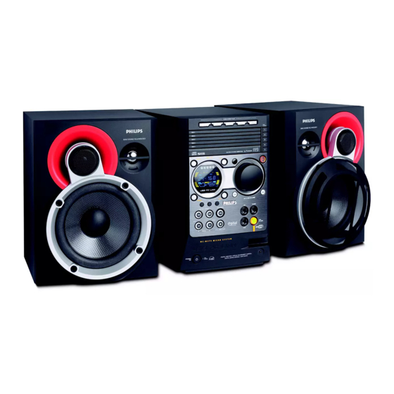
Micro System
Service
Service
Service
Service
Service
Service Manual
©
Copyright 2003 Philips Consumer Electronics B.V. Eindhoven, The Netherlands
All rights reserved. No part of this publication may be reproduced, stored in a retrieval system or
transmitted, in any form or by any means, electronic, mechanical, photocopying, or otherwise
without the prior permission of Philips.
Published by BB 0313 Service Audio
Version 1.0
TABLE OF CONTENTS
Location of pc boards & Version variations ................ 1-2
Technical Specifications ............................................. 1-3
Measurement setup .................................................... 1-4
Service Aids, Safety Instruction, etc. .......................... 1-5
Disassembly Instructions & Service positions .............. 2
Service Test Programs ............................................... 3-1
Set Block diagram ...................................................... 4-1
Set Wiring diagram ..................................................... 5-1
Front Board .................................................................... 6
ECO6 Tuner Board : Systems Non-Cenelec ............. 7A
Systems Cenelec ..................... 7B
5DTC Module (MP3 Version) ...................................... 10
Power 2003 Module (100W Class D) .......................... 11
Set Mechanical Exploded view & parts list ................. 12
Printed in The Netherlands
Subject to modification
MC-M570/
Page
CLASS 1
LASER PRODUCT
GB
21/21M/22/37
COMPACT
DIGITAL AUDIO
3139 785 30290
Advertisement
Chapters
Table of Contents

Related Manuals for Philips MC-M570/21


Summary of Contents for Philips MC-M570/21
-
Page 1: Table Of Contents
LASER PRODUCT © Copyright 2003 Philips Consumer Electronics B.V. Eindhoven, The Netherlands All rights reserved. No part of this publication may be reproduced, stored in a retrieval system or transmitted, in any form or by any means, electronic, mechanical, photocopying, or otherwise without the prior permission of Philips. - Page 2 SPECIFICATIONS GENERAL: Mains voltage : 110-127V/220-240V Switchable for /21/21M Frequency response within -3dB : 50Hz-16kHz 120V for /37 MAX Sound : On / Off 220V for /33 Digital Sound Control (DSC) : Jazz / Rock / Pop / Optimal 220-230V for /22 Virtual Environment Control (VEC) : Cyber Hall / Concert / Cinema / Off 230-240V for /30...
- Page 3 DISMANTLING INSTRUCTIONS Dismantling of the 5DTC Module Figure 3 1) Loosen 4 screws and remove the Cover Top (pos 255) by 4) To remove the Cover CD Orn (pos 111), you have to feel sliding it out towards the rear before lifting up. and give a push in the correct direction (see Figure 1) and 2 screws on the rear correct position (see Figure 2) to release the catch of the...
- Page 4 DISMANTLING INSTRUCTIONS Dismantling of the Front Panel assembly Dismantling of the Rear Panel assembly 1) Loosen 3 screws H and 2 catches C3 (see Figure 9) 1) The Knob Volume (pos 136) can be remove by pulling it out to remove the Tuner Board assembly. in the direction as shown in Figure 7.
- Page 5 DISMANTLING INSTRUCTIONS Repair Hints & Service Positions Service position B 1) During repair it is possible to disconnect the ECO6 Tuner Note: The flex cables are very fragile, care should be taken board and/or 5DTC Module completely unless the fault is not to damage them during repair.
-
Page 6: Service Test Programs
SERVICE TEST PROGRAM To start service test program ™ hold & PROG depressed while plugging in the mains cord S refers to Service Mode Display shows the V refers to Version ROM version "S-Vyy" yy refers to Software version number of the uProcessor (Main menu) (counting up from 01 to 99) Figure 1... -
Page 7: Set Block Diagram
SET BLOCK DIAGRAM +12V_M -6dB Track NOTE : +12V_A MAIN SIGNAL PATH SA BUFFER 5DTC 250mV 500mV +12V_A 125mV MEASUREMENTS ARE IN AUX MODE : FM (67.5 kHz) 76dBA ECO6 AM (80% MOD) 16dB XX mV LEVELS AT MAX VOL YY dBA S/N AT 500mW Output CONTROL... -
Page 8: Set Wiring Diagram
SET WIRING DIAGRAM FCS 1402 FCT 1012 FCT 1018 FCS 1824 5DTC 8009 9P/180mm/AD 8003 (1103) 15P/480mm/BD FOLD FCS 1401 FCT 1026 8008 19P/180mm/AD FOLD FRONT (1105A) EHT 1401 2P/260mm COMBI (1102-1001) (1104) FCS 1301 8007 FCT 1014 4P/120mm/AD EHT 1010 1302 TO BOTTOM PLATE FCT 1022... -
Page 9: Front Board
FTD DISPLAY PIN CONNECTION FRONT BOARD (1G) (2G~9G) (2G~9G) S6 S5 S4 S3 S2 S1 S1 S2 S3 S4 S5 S6 (10G) (10G) TABLE OF CONTENTS FTD Display Pin Connection ........... 6-1 Front Board - Component layout ........6-2 Front Board - Chip layout ..........6-3 Front Board - Circuit diagram (Part 1) ...... - Page 10 FRONT BOARD - CIRCUIT DIAGRAM (Part 1) 1400 F13 3508 B5 1403 A10 3509 B5 2400 A5 3510 B5 2401 A5 3511 B5 Front Board 2402 A3 3512 B5 Note : DC Voltages During Active Play. 1403 Circuit Diagram (Part 1) -33V 2403 A4 3513 B4...
- Page 11 FRONT BOARD - CIRCUIT DIAGRAM (Part 2) 1301 A7 1306 D7 1311 F8 1316 F9 1321 F7 1326 D8 2303 B6 2308 F5 2459 B4 3300 A1 3307 E2 3312 E3 3317 A6 3322 C7 3328 C8 3334 F9 3339 F7 3344 F8 3529 C2 4406 D1...
- Page 12 FRONT BOARD - CIRCUIT DIAGRAM (Part 3) 1401 A2 1402 A8 2425 E5 Front Board 2426 D8 2427 E8 Circuit Diagram (Part 3) 2428 E8 2429 F8 NON-MP3 2432 B7 1401 2433 C6 9413 2434 C6 2435 C7 GND_IIC 2436 C7 2437 E3 IIC_DATA 2438 E3...
- Page 13 CDC KEY BOARD - COMPONENT LAYOUT VARIANT TABLE Model / Version MC-500/22 MC-M570/22 MC-M570/21 MC-500/30 MC-500/25 MC-500/33 MC-M570/33 This assembly drawing shows a summary of all possible versions. For components used in a specific version see schematic diagram and respective parts list.
- Page 14 ELECTRICAL PARTS LIST - FRONT BOARD ELECTRICAL PARTS LIST - FRONT BOARD MISCELLANEOUS 1301 4822 265 11183 Flex Connector 4P 2409 4822 126 11785 47pF 5% 50V 3312 4822 117 12968 820R 5% 0,62W 3423 4822 116 52249 1k8 5% 0,5W 1302 2422 026 05059 Headphone Socket...
- Page 15 ELECTRICAL PARTS LIST - FRONT BOARD RESISTORS 3481 4822 051 30102 1k 5% 0,062W 3533 4822 052 10109 10R 5% 0,33W 3482 4822 050 11002 1k 1% 0,4W 3536 4822 051 30472 4k7 5% 0,062W 3483 4822 050 11002 1k 1% 0,4W 3537 4822 051 30472 4k7 5% 0,062W...
- Page 16 6-10 ELECTRICAL PARTS LIST - FRONT BOARD RESISTORS 4455 4822 051 30008 0R Jumper 0603 7406 4822 130 60373 BC857B 4456 4822 051 30008 0R Jumper 0603 7407 4822 209 15449 74HC4094D 4457 4822 051 30008 0R Jumper 0603 4458 4822 051 30008 0R Jumper 0603 Note :...
- Page 17 7A-1 7A-1 BLOCK DIAGRAM TUNER BOARD ECO 6 Systems Vcc1 buffer ampl. Stab Stab Discriminator FM-RF FM-IF 1 FM-IF 2 (MPX) Vcc2 1101 Loop (1102) LF filter 10,7 MHz 10,7 MHz 10,7 MHz 1120 left left Stereo right right Det. Decoder Frontend Mixer...
- Page 18 7A-2 7A-2 1101 A1 1102 B1 1103 F2 1120 E14 1130 A2 TUNER BOARD ECO6 1131 B2 / SYSTEMS NON CENELEC 1132 G13 2101 B3 VERSION PROGRAMMING COMPONENTS 2102 B1 1101 2103 C7 2105 2104 B3 AM-IF1 1130 2105 A2 100n 5111 450kHz...
- Page 19 7A-3 7A-3 1101 A6 1120 A4 1132 A5 2128 C4 2138 C2 3142 D2 5110 B3 5114 A2 5123 D5 7112 C1 9104 B5 9107 D4 TUNER ADJUSTMENT TABLE ( ECO6 FM/MW- and FM/MW/LW - versions with AM-frame aerial ) 1102 B6 1130 B5 2106 C5...
- Page 20 7A-4 7A-4 Electrical Partslist ECO6 SYSTEMS NON CENELEC MISCELLANEOUS RESISTORS ––––––––––––––––––––––––––––––––––––––––––––––––––––– ––––––––––––––––––––––––––––––––––––––––––––––––––––– 1101 2422 015 19376 SOCKET 2P CLICKFIT 3143 © 4822 051 20223 22kΩ 0,1W USA only RDS only 1102 4822 267 10283 SOCKET COAX, IEC 75Ω 3144 © 4822 051 10102 1kΩ...
-
Page 21: Systems Cenelec
7B-1 7B-1 BLOCK DIAGRAM ECO6 Tuner Board SYSTEMS CENELEC version: TABLE OF CONTENTS Blockdiagram ..............7B-1 Schematic Diagram ............7B-2 Component Layout............7B-3 Adjustment table .............7B-3 Electrical Partslist ............7B-4... - Page 22 7B-2 7B-2 1101 A2 5121 E11 1102 B1 5122 H5 1103 E2 5123 G5 1110 B2 6105-1 E4 VERSION PROGRAMMING COMPONENTS 1120 E14 6105-2 G6 TUNER BOARD ECO6 1130 A2 6106 D4 / SYSTEMS-CENELEC 1131 C2 6107 G13 VERSION AM-IF1 1132 F13 6120 C13 6120...
- Page 23 7B-3 7B-3 1101 B5 1110 B4 1131 C5 2107 B3 2133 C1 2162 A4 5102 C4 5110 A2 5114 A2 5121 B2 7104 C4 9101 A2 9104 B1 9107 B4 9110 A4 TUNER ADJUSTMENT TABLE ( ECO6 Cenelec FM/MW - and FM/MW/LW - versions with AM-frame aerial ) 1102 B5 1120 A4 1132 A4...
- Page 24 7B-4 7B-4 Electrical Partslist ECO6 SYSTEMS CENELEC MISCELLANEOUS RESISTORS DIODES ––––––––––––––––––––––––––––––––––––––––––––––––––––– ––––––––––––––––––––––––––––––––––––––––––––––––––––– ––––––––––––––––––––––––––––––––––––––––––––––––––––– 1101 2422 015 19376 SOCKET CLICKFIT 2P 3128 © 4822 117 11449 2,2kΩ 0,1W 6105 © 4822 130 83075 HN1V02H USA only LW only 1102 4822 267 10283 SOCKET COAX, IEC 75Ω...
- Page 25 10-1 5DTC Module (MP3 version) Layout stage .4 TABLE OF CONTENTS Service hints ................10-2 Location of Printed Circuit Boards ..........10-5 Wiring..................10-6 Emergency opening ..............10-7 Location of switches..............10-8 Blockdiagram ................10-9 CD B OARD Circuit Diagram ..............10-10 Component Layout side A .............10-11 Component Layout side B .............10-12 ONTROL OARD...
-
Page 26: Service Hints
10-2 Service Hints In case of symptom „skipping tracks“ perform 3. MEASURE THE EYE-PATTERN SIGNAL following actions: EYE-PATTERN SIGNAL – JITTER MEASUREMENT 1. VERIFY THE COMPLAINT Measure the signal direct on resistor 3898 using an oscilloscope (see also chapter 10-9). PLAYABILITY CHECK EYE-PATTERN Use CDDA SBC 444A: . - Page 27 10-3 Service Hints 4. MEASURE THE LASER CURRENT 6. MEASURE THE OFFSETS OF THE CD10 CD DRIVE – LASER CURRENT MEASUREMENT SIGNAL PROCESSOR – OFFSET MEASUREMENT The laser current can be measured as a voltage drop on Each ADC input of the CD10 may have an offset too. resistor 3820.
- Page 28 10-4 WARNING CHARGED CAPACITORS ON THE SERVO BOARD MAY DAMAGE THE CD DRIVE ELECTRONICS WHEN CONNECTING A NEW CDM MECHANISM. THAT´S WHY, BESIDES THE SAFETY MEASURES LIKE • SWITCH OFF POWER SUPPLY • ESD PROTECTION ADDITIONAL ACTIONS MUST BE TAKEN BY THE REPAIR TECHNICIAN. The CD drive forms a compact building block with the CD Board.
-
Page 29: Location Of Printed Circuit Boards
10-5 Location of Printed Circuit Boards CD Board MP3 Board Motor Board Control Board 5DTC Location of PCBs 2002 08 29... -
Page 30: Wiring
10-6 Wiring Diagram 5DTC Module MP3 Board Control Board 8021 Motor Board 8052 8051 1820 1825 to / from AF Board dig.out (optional) 1800 8001 CD Board 5DTC Wiring Diagram 2002 08 30 The FFC-Cables are available as sparepart. 8001 3103 308 93090 FFC CABLE 16Pin 80mm BD Connection from CD Board to CD Drive... -
Page 31: Emergency Opening
10-7 Emergency opening of the trays The trays of the 5DTC are mechanically Release snap as shown in picture 5 and pull tray out. locked. To open tray 1, 2 and 3 move lever (pos 29) backwards To remove a CD from Play Position perform following (e.g. -
Page 32: Location Of Switches
10-8 Location of switches... -
Page 33: Blockdiagram
10-9 10-9 BLOCK DIAGRAM 5DTC MP3 Version CD MECHANISM CD MAINBOARD 5,17,21,52,57 +3,3V Vref DISC 7802 1824 7887 7800 MM1469PH Vref TURNTABLE FOCB+ FOCUS CD LEFT MOTOR MOTOR Active low pass FOCB- Analog Audio Filter LM358 Vref RADB+ RADIAL CD RIGHT MOTOR RADB- SCLI... - Page 34 10-10 10-10 3912 6,1V 220R 5DTC CD BOARD 3807 3801 R2 (CD10) 7810-B 2826 3925 3873 2,4V LM358DT 3865 2851 100R LEFT LEFT CHANNEL 3926 3874 180R 2,4V 100R 3802 3808 R1 (CD10) to / from MP3 Board Active Low Pass 3803 3809 D4 (CD10)
- Page 35 10-13 10-13 5DTC CONTROL BOARD Mapping APPING FOR IRCUIT IAGRAM 1800 3832 1802 1801 3833 1800 2810 3804 3811 3824 3833 3841 3854 3862 7805-B D3 1802 3834 1801 2811 3805 3815 3826 3834 3842 3855 3863 7806 2800 3835 3826 3863 1802...
- Page 36 10-14 10-14 MP3 B OARD IRCUIT IAGRAM MP3-CD-2002 2451 B5 2452 B2 2453 B4 2454 B7 only for FLASH version 2455 C2 2456 C12 2457 D9 2450 3465 2458 C10 100n 2459 D2 100R +3.3V +core +3.3V +3.3V 2460 E13 7458 AD16 2461 D12...
- Page 37 10-16 10-16 Exploded view 5DTC mechanic - for orientation only...
- Page 38 10-17 ELECTRICAL PARTSLIST 5DTC MODULE MP3CD Version CD Board –––––––––––––––––––––––––––––––––––––––––––––––––––––––––––––––––––––––––––––––––––––––––––––––––––––––––––––––––– MECHANICAL PARTS CAPACITORS ––––––––––––––––––––––––––––––––––––––––––––––––––––– ––––––––––––––––––––––––––––––––––––––––––––––––––––– 3103 308 54710 5DTC Module (mechanic w/o electronic) 2869 © 3198 017 34730 47nF 3103 309 05390 CD DRIVE DA12T3 2870 © 4822 126 13883 220pF 4822 529 10387 Rubber damper CD DRIVE, FRONT...
- Page 39 10-18 ELECTRICAL PARTSLIST 5DTC MODULE MP3CD Version CD Board –––––––––––––––––––––––––––––––––––––––––––––––––––––––––––––––––––––––––––––––––––––––––––––––––––––––––––––––––– RESISTORS RESISTORS ––––––––––––––––––––––––––––––––––––––––––––––––––––– ––––––––––––––––––––––––––––––––––––––––––––––––––––– 3846 © 4822 051 30102 1kΩ 0,06W 3925 © 4822 051 30101 100Ω 0,06W 3847 © 4822 117 12968 820Ω 0,06W 3926 © 4822 051 30101 100Ω...
- Page 40 10-19 ELECTRICAL PARTSLIST 5DTC MODULE MP3CD Version Control Board –––––––––––––––––––––––––––––––––––––––––––––––––––––––––––––––––––––––––––––––––––––––––––––––––––––––––––––––––– MECHANICAL PARTS RESISTORS ––––––––––––––––––––––––––––––––––––––––––––––––––––– ––––––––––––––––––––––––––––––––––––––––––––––––––––– 3103 308 54710 5DTC Module (mechanic w/o electronic) 3855 © 4822 117 12706 10kΩ 0,06W 3856 © 4822 117 12706 10kΩ 0,06W MISCELLANEOUS 3857 © 4822 117 12706 10kΩ...
- Page 41 10-20 ELECTRICAL PARTSLIST 5DTC MODULE MP3CD Version MP3 Board –––––––––––––––––––––––––––––––––––––––––––––––––––––––––––––––––––––––––––––––––––––––––––––––––––––––––––––––––– MISCELLANEOUS RESISTORS ––––––––––––––––––––––––––––––––––––––––––––––––––––– ––––––––––––––––––––––––––––––––––––––––––––––––––––– 1451 2422 025 17303 FFC-CONNECTOR 19P,side entry 3484 © 4822 117 12971 15Ω 0,06W 3486 © 4822 051 30101 100Ω 0,06W CAPACITORS 3488 © 4822 117 13632 100kΩ...
- Page 42 11-1 Power 2003 Module (100W Class D) stage M.5/C.2 TABLE OF CONTENTS Brief Circuit Description ..............11-2 Service Hints ..................11-4 OMBI OARD Circuit Diagram Overview ..................11-7 Source Selector part ..............11-8 Audio Frequency & Logic part.............11-9 Oscillator & Pre-Amplifier part...........11-10 Amplifier part Left Channel ............11-11 Amplifier part Right Channel .............11-12 Component Layout Copperside view ...............11-13...
- Page 43 11-2 Class-D Circuit Description ( 2003 M -100W C ASED ON OWER ODULE LASS Basically Class-D works by transforming the LF audio input Required Circuitries: to a square wave signal with a fixed frequency and a variable duty cycle. See simplified drawing below. •...
- Page 44 11-3 Class-D Circuit Description ( 2003 M - 100W C ASED ON OWER ODULE LASS Functional Description: Protection Circuits: Refers to the left channel in schematic diagrams. The amplifier is protected against low load impedance The first stage of the modulator is an error integrator which (including short circuit).
-
Page 45: Service Hints
11-4 Service Hints The analog part of the Combi Board can be repaired without Measuring point : Output pre-amplifier opening the metal shielding box. In case of a ‘Class D’ problem it is advised to disassemble the board first, desolder the metal bottom of the shielding box and assemble the board again. - Page 46 11-5 Service Hints Measuring point Measuring point : Output modulator The first stage of the modulator is an integrator. An In this pulse width modulated square wave the analog Audio integrated rectangle results in a triangle. signal is included. Measurements with an analog scope will show a jitter on the falling edge.
- Page 47 11-6 Service Hints Measuring point : gate-signal of the FETs Measuring point Measuring point Digital output signal. Measuring point The following three signals are measured after output filter 5101 with different timebases. After common mode coil 5102 - the audio signal is restored.
-
Page 48: Combi Board
11-7 11-7 Power 2003 100W Class D Combi Board Circuit Diagram Overview OURCE ELECTOR SCILLATOR & MPLIFIER MPLIFIER ART LEFT CHANNEL Inputs: Generation of following supplies: Modulator +12V Tape / USB +5V6 Driver + Level shifter Tuner +5V_AMP Power FETs Source Selector IC + sound processing Pre-Amplifier + mute circuit Protection circuits... - Page 49 11-8 11-8 1005 1022 2528 2537 2548 2556 2564 2572 2582 3518 3526 3534 3549 3557 3566 3574 6500 6508 7505 1006 1026 2529 2538 2549 2557 2565 2573 3500 3519 3527 3535 3550 3558 3567 3575 6501 6510 7506 1010 1311 2531...
- Page 50 11-9 11-9 1004 E1 2400 B3 2408 D1 3415 E3 3433 G4 3437 H8 2404 C3 2412 E4 2416 D8 2420 H5 3402 C5 3406 C4 3410 D5 3421 F3 3425 G4 3429 G5 6400 D8 7400-B C3 7405 F4 7409 G9 9268 G8 1014 G1...
- Page 51 11-10 11-10 2224 G11 3580 F4 2300 A7 4301 A5 2301 A9 5104 A2 COMBI BOARD 2303 B6 5300 A8 2304 D3 5302 D8 & P UPPLY, SCILLATOR MPLIFIER 2305 B5 6300 E4 2306 A2 7309 B9 2334 OSCILLATOR +5V_AMP 2309 B3 7310 A3 5104...
- Page 52 11-11 11-11 2100 A10 2106 B11 2113 D8 2118 F10 2124 F10 2132 C4 3100 A2 3107 D7 3115 E5 3122 C4 3129 F10 3136 E11 3142 F7 3148 F2 3154 B7 5101 D11 6109 B7 7104 B11 7105-E B7 7114 C8 7118-C F7 7121 E10...
- Page 53 11-12 11-12 1201 E14 2200 A10 2208 A4 2214 D8 2220 F10 2229 G9 2240 A6 3205 B9 3215 B9 3223 C12 3229 D13 3240 E11 3248 E10 3256 F5 3264 C8 4202 E11 6104 G12 6210 D8 6217 F6 7209-B B7 7211 B12 7227 F10...
- Page 54 11-16 11-16 0201 D10 1207 B5 1222 A2 2204 A6 2210 C7 2215 D5 2220 E1 2226 D7 2233 A7 3204 A2 3212 D5 3219 E6 5001 A4 6201 C9 6209 C6 6215 D8 6221 E8 6226 E2 7203 D3 9201 B3 1201 A3 1208 C3...
- Page 55 11-17 MAINS BOARD ELECTRICAL PARTSLIST POWER 2003 100W Class-D –––––––––––––––––––––––––––––––––––––––––––––––––––––––––––––––––––––––––––––––––––––––––––––––––––––––––––––––––– MISCELLANEOUS COILS ––––––––––––––––––––––––––––––––––––––––––––––––––––– ––––––––––––––––––––––––––––––––––––––––––––––––––––– ! 4822 071 51602 1201 FUSE 1,6A 5202 4822 157 53473 1000µH 1201 ! 4822 253 10126 FUSE T4A 5203 4822 157 53473 1000µH 1203 ! 4822 071 55002 5220 ! 4822 157 11832 FUSE T5A 400µH Mains filter...
- Page 56 11-18 COMBI BOARD ELECTRICAL PARTSLIST POWER 2003 100W Class-D –––––––––––––––––––––––––––––––––––––––––––––––––––––––––––––––––––––––––––––––––––––––––––––––––––––––––––––––––– MECHANICAL PARTS CAPACITORS ––––––––––––––––––––––––––––––––––––––––––––––––––––– ––––––––––––––––––––––––––––––––––––––––––––––––––––– 0021 4822 492 11735 SPRING TRANSISTOR 2219 © 5322 126 11578 2220 © 5322 126 11578 MISCELLANEOUS 2221 © 4822 126 13193 4,7nF ––––––––––––––––––––––––––––––––––––––––––––––––––––– 2222 © 3198 017 41050 1µF 1005 2422 026 05418...
- Page 57 11-19 COMBI BOARD ELECTRICAL PARTSLIST POWER 2003 100W Class-D –––––––––––––––––––––––––––––––––––––––––––––––––––––––––––––––––––––––––––––––––––––––––––––––––––––––––––––––––– CAPACITORS RESISTORS ––––––––––––––––––––––––––––––––––––––––––––––––––––– ––––––––––––––––––––––––––––––––––––––––––––––––––––– 2418 © 2020 552 94427 100pF 3111 © 4822 051 30682 6,8kΩ 0,06W 2419 © 2020 552 94427 100pF 3112 © 4822 117 12925 47kΩ 0,06W 2420 ©...
- Page 58 11-20 COMBI BOARD ELECTRICAL PARTSLIST POWER 2003 100W Class-D –––––––––––––––––––––––––––––––––––––––––––––––––––––––––––––––––––––––––––––––––––––––––––––––––––––––––––––––––– RESISTORS RESISTORS ––––––––––––––––––––––––––––––––––––––––––––––––––––– ––––––––––––––––––––––––––––––––––––––––––––––––––––– 3238 © 4822 051 30103 10kΩ 0,06W 3344 © 4822 051 30471 470Ω 0,06W 3239 © 4822 117 12139 22Ω 0,06W 3345 © 4822 051 30471 470Ω...
- Page 59 11-21 COMBI BOARD ELECTRICAL PARTSLIST POWER 2003 100W Class-D –––––––––––––––––––––––––––––––––––––––––––––––––––––––––––––––––––––––––––––––––––––––––––––––––––––––––––––––––– RESISTORS COILS ––––––––––––––––––––––––––––––––––––––––––––––––––––– ––––––––––––––––––––––––––––––––––––––––––––––––––––– 3551 © 4822 051 30101 100Ω 0,06W 5100 4822 526 10494 FERRITE BEAD 3552 © 4822 051 30101 100Ω 0,06W 5101 2422 536 00612 30µH 3553 © 4822 051 30101 100Ω...
- Page 60 11-22 COMBI BOARD ELECTRICAL PARTSLIST POWER 2003 100W Class-D –––––––––––––––––––––––––––––––––––––––––––––––––––––––––––––––––––––––––––––––––––––––––––––––––––––––––––––––––– TRANSISTORS ––––––––––––––––––––––––––––––––––––––––––––––––––––– 7203 © 3198 010 42310 BC847BW 7208 © 4822 130 60373 BC856B 7210 © 3198 010 44350 BC807-25W 7211 © 3198 010 42320 BC857BW 7218 ! 9322 173 29687 STP14NF12FP Power FET 7221 ©...