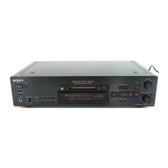
Sony MDS-JB940 Service Manual
Minidisc deck
Hide thumbs
Also See for MDS-JB940:
- Operating instructions manual (120 pages) ,
- Operating instruction (59 pages) ,
- Specifications (2 pages)
Table of Contents
Advertisement
SERVICE MANUAL
U.S and foreign patents licensed from Dolby
Laboratories Licensing Corporation.
System
MiniDisc digital audio system
Disc
MiniDisc
Laser
Semiconductor laser (λ = 780 nm)
Emission duration: continuous
MAX 44.6 µW
Laser output
1)
1) This output is the value
measured at a distance of
200 mm from the objective lens
surface on the Optical Pick-up
Block with 7 mm aperture.
Laser diode
Material: GaAlAs
Revolutions (CLV)
400 rpm to 900 rpm
Error correction
ACIRC (Advanced Cross Interleave
Reed Solomon Code)
Sampling frequency
44.1 kHz
Coding
ATRAC (Adaptive TRansform
Acoustic Coding)/ATRAC 3
Modulation system
EFM (Eight-to-Fourteen
Modulation)
Number of channels
2 stereo channels
5 to 20,000 Hz ±0.3 dB
Frequency response
Signal-to-noise ratio
Over 100 dB during play
Wow and flutter
Below measurable limit
Inputs
ANALOG IN
Jack type: phono
Impedance: 47 kilohms
Rated input: 500 mVrms
Minimum input: 125 mVrms
MDS-JB940
Model Name Using Similar Mechanism
MD Mechanism Type
Optical Pick-up Name
SPECIFICATIONS
DIGITAL OPTICAL IN1 Connector type: square optical
Impedance: 660 nm (optical wave
length)
DIGITAL OPTICAL IN2 Connector type: square optical
Impedance: 660 nm (optical wave
length)
DIGITAL COAXIAL IN
Jack type: phono
Impedance: 75 ohms
Rated input: 0.5 Vp-p, ±20 %
Outputs
PHONES
Jack type: stereo phone
Rated output: 28 mW
Load impedance: 32 ohms
ANALOG OUT
Jack type: phono
Rated output: 2 Vrms (at 50
kilohms)
Load impedance: over 10 kilohms
DIGITAL OPTICAL OUT Connector type: square optical
Rated output: –18 dBm
Load impedance: 660 nm (optical
wave length)
DIGITAL COAXIAL OUT Jack type: phono
Rated output: 0.5 Vp-p (at 75 ohms)
Load impedance: 75 ohms
US Model
Canadian Model
AEP Model
UK Model
NEW
MDM-7A
KMS-260B/J1N
General
Power requirements
Where purchased
Power requirements
U.S.A. and Canada
120 V AC, 60 Hz
Europe
230 V AC, 50/60 Hz
Power consumption
18 W
430 × 111 × 286 mm (17 × 4
Dimensions (approx.)
11
3
/
in.) (w/h/d) incl. projecting
8
parts and controls
Mass (approx.)
5.3 kg (11 lbs 11 oz)
Supplied accessories
This MD deck comes with the following items:
Audio connecting cords (2)
Optical cable (1)
Remote commander (remote) (1)
R6 (size-AA) batteries (2)
US and foreign patents licensed from Dolby Laboratories.
Design and specifications are subject to change without
notice.
MINIDISC DECK
×
3
/
8
Advertisement
Table of Contents

Related Manuals for Sony MDS-JB940


Summary of Contents for Sony MDS-JB940
-
Page 1: Specifications
MDS-JB940 SERVICE MANUAL US Model Canadian Model AEP Model UK Model Model Name Using Similar Mechanism U.S and foreign patents licensed from Dolby Laboratories Licensing Corporation. MD Mechanism Type MDM-7A Optical Pick-up Name KMS-260B/J1N SPECIFICATIONS System MiniDisc digital audio system... -
Page 2: Table Of Contents
TABLE OF CONTENTS SAFETY CHECK-OUT SELF-DIAGNOSIS FUNCTION After correcting the original service problem, perform the ········································ 4 following safety checks before releasing the set to the customer: Check the antenna terminals, metal trim, “metallized” knobs, screws, 1. SERVICE NOTE ······························································· 6 and all other exposed metal parts for AC leakage. - Page 3 CRITIQUES POUR LA SÉCURITÉ DE FONCTIONNEMENT. NE COMPONENTS WITH SONY PARTS WHOSE PART NUMBERS REMPLACER CES COMPOSANTS QUE PAR DES PIÈSES SONY APPEAR AS SHOWN IN THIS MANUAL OR IN SUPPLEMENTS DONT LES NUMÉROS SONT DONNÉS DANS CE MANUEL OU PUBLISHED BY SONY.
-
Page 4: Self-Diagnosis Function
The deck’s self-diagnosis function automatically checks the condition of the MD deck when an error occurs, then issues a three- or five-digit code and an error message on the display. If the code and message alternate, find them in the following table and perform the indicated countermeasure. Should the problem persist, consult your nearest Sony dealer. Three- or five-... - Page 5 [ITEMS OF ERROR HISTORY MODE ITEMS AND CONTENTS] Display Details of History op rec tm Displays the total recording time. When the total recording time is one minute or longer, displays the time and minute. When the total recording time is less than one minute, displays “Under 1 min”. The displayed time is about 1/4 of the actual recording time when the laser is set to the high power state.
-
Page 6: Service Note
SECTION 1 SERVICE NOTE JIG FOR CHECKING BD BOARD WAVEFORM The special jig (J-2501-196-A) is useful for checking the waveform of the BD board. The names of terminals and the checking items to be performed are shown as follows. GND : Ground I+3V : For measuring IOP (Check the deterioration of the optical pick-up laser) IOP : For measuring IOP (Check the deterioration of the optical pick-up laser) TEO : TRK error signal (Traverse adjustment) - Page 7 IOP DATA RECORDING AND DISPLAY WHEN OPTICAL PICK-UP AND NON-VOLATILE MEMORY (IC195 OF BD BOARD) ARE REPLACED The IOP value labeled on the optical pick-up can be recorded in the non-volatile memory. By recording the value, it will eliminate the need to look at the value on the optical pick-up label.
- Page 8 CHECKS PRIOR TO PARTS REPLACEMENT AND ADJUSTMENTS Before performing repairs, perform the following checks to determine the faulty locations up to a certain extent. Details of the procedures are described in “5. Electrical Adjustments”. Criteria for Determination Measure if unsatisfactory: (Unsatisfactory if specified value is not satisfied) Laser power check •...
- Page 9 RETRY CAUSE DISPLAY MODE • In this test mode, the causes for retry of the unit during recording can be displayed on the fluorescent indicator tube. During playback, the “track mode” for obtaining track information will be set. This is useful for locating the faulty part of the unit. •...
- Page 10 Reading the Retry Cause Display Higher Bits Lower Bits Details Hexa- Hexadecimal decimal When 0 When 1 b7 b6 b5 b4 b3 b2 b1 b0 Binary Emphasis OFF Emphasis ON Monaural Stereo This is 2-bit display. Normally 01. 01:Normal audio. Others:Invalid Audio (Normal) Invalid Original...
-
Page 11: General
SECTION 2 This section is extracted from instruction manual. GENERAL... -
Page 14: Disassembly
SECTION 3 DISASSEMBLY Note : Follow the disassembly procedure in the numerical order given. 3-1. CASE (4095269) 1 Four screws (Screw (TP), flat head) 3 Case (4095269) 2 Three screws (Screw (TP), flat head) 3-2. FRONT PANEL SECTION 2 Connector (CN801) 1 Connector (CN800) - Page 15 3-3. AU BOARD 5 Connector (CN401) 4 Connector (CN403) 9 Screw (BVTP 3 × 8) 3 Connector (CN404) 8 Wire (flat type) (23 core) (CN11) 2 Connector (CN200) 6 Connector (CN700) q; Four screws (BVTP 3 × 8) 7 Wire (flat type) (27 core) (CN12) 1 Wire (flat type) (19 core) (CN2)
- Page 16 3-4. MECHANISM DECK (MDM-7A) 2 Wire (flat type)(23 core)(CN11) 3 Four step screws (BVTTWH M3) 1 Wire (flat type) (27 core) (CN12) 4 Remove the mechanism deck (MDM-7A) to direction of the arrow. 3-5. BD BOARD 5 Remove the solder (four portions) 1 Wire (flat type)(23 core) 2 Wire (flat type) (27 core)
-
Page 17: Test Mode
SECTION 4 TEST MODE 4-1. PRECAUTIONS FOR USE OF TEST MODE • As loading related operations will be performed regardless of the test mode operations being performed, be sure to check that the disc is stopped before setting and removing it. Even if the EJECT A button is pressed while the disc is rotating during continuous playback, continuous recording, etc., the disc will not stop rotating. - Page 18 4-5. SELECTING THE TEST MODE There are 25 types of test mode as shown below. The groups can be switched by turning the l AMS L knob. All of the service adjustments and checks can be performed in the test modes of Service group. There is also the Develop group, but it is not used for service.
- Page 19 4-5-1. Operating the Continuous Playback Mode 1. Entering the continuous playback mode Set the disc in the unit. (Whichever recordable discs or discs for playback only are available.) Turn the l AMS L knob and display “CPLAY 1 MODE” (C35). Press the YES button to change the display to “CPLAY 1 MID”.
- Page 20 4-6. FUNCTIONS OF OTHER BUTTONS Function Contents PLAY Sets continuous playback when pressed in the STOP state. When pressed during continuous playback, the tracking servo turns ON/OFF. STOP Stops continuous playback and continuous recording. The sled moves to the outer circumference only when this is pressed. The sled moves to the inner circumference only when this is pressed.
- Page 21 4-8. MEANINGS OF OTHER DISPLAYS Contents Display When Lit When Off Servo ON Servo OFF Tracking servo OFF Tracking servo ON Recording mode ON Recording mode OFF SYNC (other models/TOC EDIT) CLV low speed mode CLV normal mode L. SYNC (other models/A.SPACE) ABCD adjustment completed OVER Tracking offset cancel ON...
-
Page 22: Electrical Adjustments
SECTION 5 ELECTRICAL ADJUSTMENTS 5-1. PARTS REPLACEMENT AND ADJUSTMENT If a defect such as dropout caused by the OP is found, check the following. Check Procedure Before Replacement Start Laser power check Iop Compare Replace the OP AUTO CHECK or replace the MDM. - Page 23 Flow During Adjustment Start After turning on the power again, initialize Replace IC195. EEPROM. Replace either OP or IC195. ADJ CLEAR Replace either IC101, IC195 or D101. TEMP ADJUST Replace either OP, IC190 or IC195. LDPWR ADJUST Replace either Iop NV Save OP, IC102, IC190 or IC195.
- Page 24 5-2. PRECAUTIONS FOR CHECKING LASER Use the following tools and measuring devices. • Check Disc (MD) TDYS-1 DIODE EMISSION (Part No. 4-963-646-01) To check the emission of the laser diode during adjustments, never • Test Disc (MDW-74/GA-1) (Part No. 4-229-747-01) view directly from the top as this may lose your eye-sight.
- Page 25 5-6. CHECK PRIOR TO REPAIRS Press the MENU/NO button to display “LDPWR CHECK” and stop the laser emission. These checks are performed before replacing parts to determine the (The MENU/NO button is effective at all times to stop the faulty locations. laser emission) 5-6-1.
- Page 26 5-6-5. Other Checks 11. Press the YES button to display “EF MO CHECK” All of the following check modes have already been checked in the The disc stops rotating automatically. 12. Press the EJECT A button and take out the disc. section “AUTO CHECK”.
- Page 27 3. C PLAY Checking 5-8. RECORDING AND DISPLAYING THE IOP INFORMATION a. MO Error Rate Check The IOP data can be recorded in the non-volatile memory. The IOP Checking Procedure : value on the optical pick-up label and the IOP value after the Load the recorded test disk (MDW-74/GA-1).
- Page 28 5-10. LASER POWER ADJUSTMENT 12. Press the YES button. When the display becomes Ref=@@@.@ (@ is an arbitrary number), press the YES Check the IOP value of the optical pick-up before adjustments. button to display “Measu=@@@.@” (@ is an arbitrary (Refer to 5-8.
- Page 29 5-12. TRAVERSE ADJUSTMENT 11. Turn the l AMS L knob until the waveform of the oscilloscope moves closer to the specified value. Connection: In this adjustment, waveform varies at intervals of approx. 2%. Oscilloscope Adjust the waveform so that the specified value is satisfied as (DC range) much as possible.
- Page 30 5-13. FOCUS BIAS ADJUSTMENT 5-15. FOCUS BIAS CHECK Change the focus bias and check the focus tolerance amount. Adjusting Procedure : Load the continuously-recorded disc (MDW-74/GA-1). Checking Procedure : (Refer to “5-5. Creating Continuously-Recorded Disc”) Load the continuously-recorded disc (MDW-74/GA-1). (Refer Turn the l AMS L knob to display “CPLAY 1 MODE”...
-
Page 31: Diagrams
MDS-JB940 SECTION 6 DIAGRAMS 6-1. BLOCK DIAGRAM MAIN Section IC303 IC301 IC301 DIGITAL INPUT OPTICAL IC302 IC300 IC301 IC301 DIGITAL INPUT IC151(1/2) DIN0 J300 HR901 IC301 IC301 OVER WRITE COAXIAL HEAD EFMO DIGITAL OVER WRITE OVER WRITE HEAD DRIVE HEAD DRIVE... -
Page 32: Display/Power Section
MDS-JB940 6-2. BLOCK DIAGRAM DISPLAY/POWER Section P DOWN MAIN SECTION DISPLAY CONTROL FL781 REGULATOR IC1(2/2) FL DRIVER IC400 FLOURESCENT IC771 J801 IIC CLK INDICATOR TUBE P DOWN KEYBOARD RESET D/A +5V LF901 PANEL +5V TR900 DATA(FL) PH5V D904-907 CLK(FL) SEG01... -
Page 33: Note For Printed Wiring Boards And Schematic Diagrams
6-3. NOTE FOR PRINTED WIRING BOARDS AND SCHEMATIC DIAGRAMS (In addition to this, the necessary note is printed in each block) Note on Printed Wiring Board: Note on Schematic Diagram: • X : parts extracted from the component side. • All capacitors are in µF unless otherwise noted. pF: µµF : Through hole. -
Page 34: Waveforms
6-5. WAVEFORMS – BD Board – – MAIN Board – IC101 ek (RF) IC1 w; (XOUT) 3 Vp-p 1.3 Vp-p 10 MHz IC101 ef (FE) IC1 qk (CLOCK) (PLAY MODE) 1.6 Vp-p 0.2 Vp-p 32.768 MHz IC101 wh (TE) IC201 qs (XOUT) (PLAY MODE) 5.2 Vp-p 45.158 MHz... -
Page 35: Printed Wiring Board
MDS-JB940 6-6. PRINTED WIRING BOARD BD Board • See page 33 for Circuit Board Location. (KMS-260B/J1N) • Semiconductor Location Ref. No. Location Ref. No. Location D101 A-1 (A) Q101 B-1 (A) D181 D-3 (B) Q121 B-3 (B) D183 D-3 (B) -
Page 36: Bd Board (1/2)
MDS-JB940 • See page 34 for Waveforms. 6-7. SCHEMATIC DIAGRAM BD Board (1/2) • See page 48 for IC Block Diagrams. • See page 53 for IC Pin Function. (KMS-260B/J1N) PIN FUNCTION... -
Page 37: Bd Board (2/2)
MDS-JB940 6-8. SCHEMATIC DIAGRAM BD Board (2/2) • See page 34 for Waveforms. • See page 49 for IC Block Diagrams. • See page 54 for IC Pin Function. PIN FUNCTION (Page 39) (Page 40) -
Page 38: Hp Board/Key Board
MDS-JB940 • See page 33 for Circuit Board Location. • See page 52 for IC Block Diagram. 6-9. PRINTED WIRING BOARD HP Board/KEY Board 6-10. SCHEMATIC DIAGRAM HP Board/KEY Board There are few cases that the part printed on this diagram isn’t mounted in this model. -
Page 39: Schematic Diagram
MDS-JB940 6-11. SCHEMATIC DIAGRAM MAIN Board (1/3) • See page 34 for Waveforms. • See page 57 for IC Pin Function. (Page 38) (Page 45) PIN FUNCTION (Page 37) -
Page 40: Main Board (2/3)
MDS-JB940 • See page 50 for IC Block Diagrams. 6-12. SCHEMATIC DIAGRAM MAIN Board (2/3) (Page 46) (Page 37) (Page 46) (Page 46) -
Page 41: Main Board (3/3)
MDS-JB940 6-13. SCHEMATIC DIAGRAM MAIN Board (3/3) • See page 34 for Waveforms. • See page 50 for IC Block Diagrams. (Page 38) -
Page 42: Main Board (Side A)
MDS-JB940 • See page 33 for Circuit Board Location. 6-14. PRINTED WIRING BOARD MAIN Board (Side A) There are few cases that the part printed on this diagram isn’t mounted in this model. Note: * Stand C604 vertically. (Page 47) -
Page 43: Printed Wiring Board
MDS-JB940 6-15. PRINTED WIRING BOARD MAIN Board (Side B) • See page 33 for Circuit Board Location. There are few cases that the part printed on this diagram isn’t mounted in this model. • Semiconductor Location Ref. No. Location D201... -
Page 44: Panel Section
MDS-JB940 • See page 33 for Circuit Board Location. 6-16. PRINTED WIRING BOARD PANEL Section There are few cases that the part printed on this diagram isn’t mounted in this model. (Page 43) -
Page 45: Schematic Diagram
MDS-JB940 6-17. SCHEMATIC DIAGRAM PANEL Section (Page 39) -
Page 46: Ac Board
MDS-JB940 6-18. SCHEMATIC DIAGRAM AC Board (Page 40) IC902 (Page 40) (Page 40) -
Page 47: Printed Wiring Board
MDS-JB940 6-19. PRINTED WIRING BOARD AC Board • See page 33 for Circuit Board Location. There are few cases that the part printed on this diagram isn’t mounted in this model. (Page 42) -
Page 48: Ic Block Diagrams
6-20. IC BLOCK DIAGRAMS – BD Board – IC101 CXA2523AR 43 42 USROP – RF AGC – USRC RFA1 BPF3T RFA2 RFA3 PEAK3T – HLPT –1 – – –2 – OFST PTGR TEMP PEAK – –2 – 36 BOTM BOTTOM –... - Page 49 IC151 CXD2662R 100 99 98 97 96 95 94 93 92 91 90 89 88 87 86 85 84 83 82 81 80 79 78 77 76 SPINDLE GENERATOR SERVO 75 TE MNT0 74 SE MNT1 EACH MONITOR 73 AVSS BLOCK CONTROL MNT2...
- Page 50 – AU Board – IC603 AK4524-TP IC301 SN74HCU04ANSR VCOM AINR AOUTR+ AOUTR– CONVERTER CONVERTER AOUTL+ BLOCK BLOCK AOUTL– AINL VREF AGND DGND TEST XTAO CLOCK XTAI GENERATOR CLKO & DIVIDER XTALE 10 H.P.F. LRCK 11 D-ATT CONTROL AUDIO BICK 12 REGISTER INTERFACE SDTO 13...
- Page 51 IC201 CXD9556AQ 4BIT DATA CKTL2 DINIT MUTE 1FS or / INIT CKTL1 INAF CKTL0 OVFLAG CLOCK GEN. TEST2 CKVDD DIGITAL FILTER TEST1 CTLVDD DFIOSEL SYNC DFLRCK MODE DFDTL SCDATA SERIAL DFDTR SHIFT LINEAR CONTROL INTERPOLATOR DFBCK LATCH & 64FS NOISE SHAPER DFDTEN INIT 128FS...
- Page 52 IC400 LA5643 – STBY ANA5 – SYS3.3 – – 3.3V B.BAK – DELAY P. DOWN CIRCUIT – DELAY S. RESET CIRCUIT VREF – HP Board – IC802 M5218AL V–...
-
Page 53: Ic Pin Function Description
6-21. IC PIN FUNCTION DESCRIPTION • BD BOARD IC101 CXA2523AR (RF AMP, FOCUS/TRACKING ERROR AMP) Pin No. Pin Name Description I-V converted RF signal I input from the optical pick-up block detector I-V converted RF signal J input from the optical pick-up block detector Middle point voltage (+1.65V) generation output terminal 4 to 9 A to F... - Page 54 BD BOARD IC151 CXD2656R (DIGITAL SIGNAL PROCESSOR, DIGITAL SERVO PROCESSOR, EFM/ACIRC ENCODER/DECODER, SHOCK PROOF MEMORY CONTROLLER, ATRAC ENCODER/DECODER) Pin No. Pin Name Description Focus OK signal output to the system controller (IC800) MNT0 (FOK) “H” is output when focus is on (“L”: NG) MNT1 (SHOCK) Track jump detection signal output to the system controller (IC800) MNT2 (XBUSY)
- Page 55 Pin No. Pin Name Description XCAS Column address strobe signal output to the D-RAM (IC124) “L” active Address signal output to the D-RAM (IC124) XRAS Row address strobe signal output to the D-RAM (IC124) “L” active Write enable signal output to the D-RAM (IC124) “L” active Two-way data bus with the D-RAM (IC124) I (S) MVCI...
- Page 56 Pin No. Pin Name Description FRDR Focus servo drive PWM signal (–) output to the BH6511FS (IC152) Clock signal (176.4 kHz) output terminal (X’tal system) Not used (open) SRDR Sled servo drive PWM signal (–) output to the BH6511FS (IC152) SFDR Sled servo drive PWM signal (+) output to the BH6511FS (IC152) SPRD...
- Page 57 AU BOARD IC1 M30805SGP (SYSTEM CONTROL) Pin No. Pin Name Description FL-DATA Display tube, serial data (TxD4) for display by microprocessor FL-CLK Display tube, serial clock (CLC4) for display by microprocessor A1-IN Control A1 input Remote control data input Not used FL-REQ Not used FL-BUSY...
- Page 58 Pin No. Pin Name Description Not used (fixed to High) Microprocessor mode HOLD Not used (fixed to High) HLDA Microprocessor mode MNT2(XBUSY) (DSP) Power supply ground MNT1(SHCK) (DSP) 3.3 V power supply EEP-WP EEP-ROM write protect SDA(EEP) EEP data BCLK Not used Read signal output Not used...
- Page 59 Pin No. Pin Name Description TIMER Timer mode selection (slide switch) 137 to 139 KEY3 to 1 Key input AVSS Power supply ground KEY0 Key input VREF 3.3 V power supply AVCC 3.3 V power supply FL-DATA(IN) Not used...
-
Page 60: Exploded Views
SECTION 7 EXPLODED VIEWS NOTE: • -XX, -X mean standardized parts, so they may • Hardware (# mark) list and accessories and The components identified by mark 0 or have some differences from the original one. packing materials are given in the last of this dotted line with mark 0 are critical for safety. - Page 61 A-4725-114-A SW BOARD,COMPLETE 4-227-839-71 PANEL, FRONT (BLACK) (US,CND) A-4725-110-A DISP BOARD,COMPLETE 4-228-518-01 WINDOW (RM) A-4725-111-A PSW BOARD,COMPLETE 4-942-568-41 EMBLEM (NO.5), SONY (BLACK) 1-678-501-11 KEY BOARD 4-942-568-61 EMBLEM (NO.5), SONY (SILVER) 1-677-836-11 HP BOARD 4-998-607-01 INDICATOR (POWER) 4-951-620-01 SCREW (+BVTP 2.6X8)
- Page 62 7-3. MECHANISM-1 SECTION (MDM-7A) not supplied not supplied not supplied Ref. No. Part No. Description Remarks Ref. No. Part No. Description Remarks * 201 4-996-267-01 BASE (BU-D) 4-229-533-01 SPRING (STOPPER), TORSION 4-908-618-21 SCREW (+BTP) (2X6) 4-227-012-01 SPRING (HOLDER), TENSION 4-227-007-01 GEAR (SB) 4-227-019-01 PLATE (HOLDER), RETAINER 4-227-025-01 BELT (LOADING) 4-227-013-01 SPRING (EJ), TENSION...
- Page 63 7-4. MECHANISM-1 SECTION (MDM-7A) HR901 S102 M101 M102 M103 Ref. No. Part No. Description Remarks Ref. No. Part No. Description Remarks A-4725-054-A BD BOARD,COMPLETE 4-211-036-01 SCREW (1.7X2.5), +PWH 4-908-618-21 SCREW (+BTP) (2X6) 4-226-990-01 BASE (BU-A) 3-372-761-01 SCREW (M1.7), TAPPING 4-227-023-01 SPRING (SPINDLE), TORSION 4-226-993-01 RACK 4-227-004-01 GEAR (LC) 4-227-014-01 SPRING (RACK), COMPRESSION...
- Page 64 SECTION 8 ELECTRICAL PARTS LIST NOTE: • Due to standardization, replacements in the • RESISTORS • CAPACITORS: parts list may be different from the parts All resistors are in ohms. uF: µF specified in the diagrams or the components METAL: metal-film resistor •...
- Page 65 Ref. No. Part No. Description Remarks Ref. No. Part No. Description Remarks < RESISTOR > C215 1-165-319-11 CERAMIC CHIP 0.1uF C217 1-165-319-11 CERAMIC CHIP 0.1uF R907 1-249-441-11 CARBON 100K 1/4W C218 1-124-997-11 ELECT 470uF 20.00% 6.3V R908 1-249-441-11 CARBON 100K 1/4W C219 1-124-997-11 ELECT...
- Page 66 Ref. No. Part No. Description Remarks Ref. No. Part No. Description Remarks C318 1-136-165-00 MYLAR 0.1uF 5.00% 50V C646 1-163-251-11 CERAMIC CHIP 100PF 5.00% 50V C319 1-163-251-11 CERAMIC CHIP 100PF 5.00% 50V C647 1-163-251-11 CERAMIC CHIP 100PF 5.00% 50V C320 1-125-827-91 CERAMIC CHIP 10.00% 25V C648...
- Page 67 Ref. No. Part No. Description Remarks Ref. No. Part No. Description Remarks IC206 8-759-712-02 IC NJM2114D L463 1-414-235-22 INDUCTOR CHIP 0uH IC255 8-759-712-02 IC NJM2114D L601 1-414-235-22 INDUCTOR CHIP 0uH IC256 8-759-712-02 IC NJM2114D L603 1-412-056-11 INDUCTOR CHIP 4.7uH IC300 8-759-926-17 IC SN74HC153ANSR L604 1-414-235-22 INDUCTOR CHIP 0uH...
- Page 68 Ref. No. Part No. Description Remarks Ref. No. Part No. Description Remarks R124 1-216-073-00 METAL CHIP 1/10W R275 1-216-295-91 SHORT R134 1-216-073-00 METAL CHIP 1/10W R276 1-216-295-91 SHORT R135 1-216-073-00 METAL CHIP 1/10W R277 1-216-663-11 METAL CHIP 3.3K 0.5% 1/10W R136 1-216-073-00 METAL CHIP 1/10W...
- Page 69 Ref. No. Part No. Description Remarks Ref. No. Part No. Description Remarks R603 1-216-687-11 METAL CHIP 0.5% 1/10W C106 1-162-970-11 CERAMIC CHIP 0.01uF R605 1-216-679-11 METAL CHIP 0.5% 1/10W C107 1-162-970-11 CERAMIC CHIP 0.01uF R607 1-216-627-11 METAL CHIP 0.5% 1/10W C108 1-162-969-11 CERAMIC CHIP 0.0068uF 10%...
- Page 70 Ref. No. Part No. Description Remarks Ref. No. Part No. Description Remarks C192 1-164-156-11 CERAMIC CHIP 0.1uF L183 1-216-296-91 SHORT C193 1-126-206-11 ELECT CHIP 100uF 6.3V L184 1-216-296-91 SHORT C194 1-164-156-11 CERAMIC CHIP 0.1uF C195 1-164-156-11 CERAMIC CHIP 0.1uF < TRANSISTOR > C196 1-164-156-11 CERAMIC CHIP 0.1uF...
- Page 71 DISP Ref. No. Part No. Description Remarks Ref. No. Part No. Description Remarks R155 1-216-864-11 METAL CHIP 1/16W C783 1-124-261-00 ELECT 10uF R156 1-216-864-11 METAL CHIP 1/16W C784 1-124-261-00 ELECT 10uF R157 1-216-809-11 METAL CHIP 1/16W R158 1-216-809-11 METAL CHIP 1/16W <...
- Page 72 Ref. No. Part No. Description Remarks Ref. No. Part No. Description Remarks < IC > A-4725-111-A PSW BOARD, COMPLETE ******************** IC802 8-759-634-50 IC M5218AL < CAPACITOR > < JACK > C731 1-162-294-31 CERAMIC 0.001uF J802 1-770-307-11 JACK (LARGE TYPE)(PHONES) C751 1-164-159-11 CERAMIC 0.1uF C752...
- Page 73 Ref. No. Part No. Description Remarks Ref. No. Part No. Description Remarks A-4725-114-A SW BOARD, COMPLETE MISCELLANEOUS ******************* ************* < CAPACITOR > 1-792-926-11 WIRE(FLAT TYPE) (19 CORE) 1-792-925-11 WIRE(FLAT TYPE) (23 CORE) C700 1-124-589-11 ELECT 47uF 1-792-810-11 WIRE(FLAT TYPE) (27 CORE) C701 1-162-294-31 CERAMIC 0.001uF...
- Page 74 MDS-JB940 Sony Corporation 9-929-274-11 2000F1661-1 Audio Entertainment Group Printed in Japan © 2000.6 Published by HA Quality Assurance Dept.