Sony MDS-JA30ES Service Manual
Minidisc deck
Hide thumbs
Also See for MDS-JA30ES:
- Operating instructions manual (88 pages) ,
- Operating instructions manual (85 pages) ,
- Limited warranty (1 page)
Table of Contents
Advertisement
Quick Links
SERVICE MANUAL
U.S. and foreign patents licensed from Dolby Laboratories
Licensing Corporation.
MICROFILM
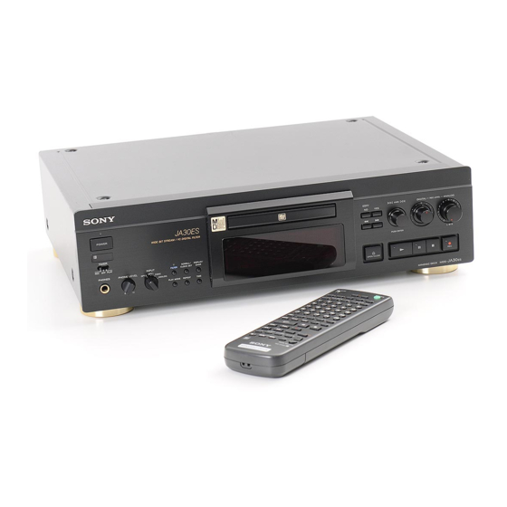
MDS-JA30ES
Photo: GOLD
Model Name Using Similar Mechanism
MD Mechanism Type
Base Unit Type
Optical Pick-up Type
SPECIFICATIONS
US Model
Canadian Model
AEP Model
UK Model
MDS-JA50ES
MDM-4B
MBU-2B
KMS-210A/J-N
— Continued on next page —
MINIDISC DECK
Advertisement
Table of Contents

Related Manuals for Sony MDS-JA30ES


Summary of Contents for Sony MDS-JA30ES
- Page 1 MDS-JA30ES SERVICE MANUAL US Model Canadian Model AEP Model UK Model Photo: GOLD U.S. and foreign patents licensed from Dolby Laboratories Model Name Using Similar Mechanism MDS-JA50ES Licensing Corporation. MD Mechanism Type MDM-4B Base Unit Type MBU-2B Optical Pick-up Type...
- Page 2 DIAGRAMMES SCHÉMATIQUES ET LA LISTE DES PIÈCES SONT CRITIQUES POUR LA SÉCURITÉ DE FONCTIONNEMENT. NE VAROITUS REMPLACER CES COMPOSANTS QUE PAR DES PIÈSES SONY DONT LES NUMÉROS SONT DONNÉS DANS CE MANUEL OU Parist voi räjähtää, jos se on virheellisesti asennettu.
-
Page 3: Table Of Contents
TABLE OF CONTENTS The laser component in this product is capable of emitting radiation exceeding SERVICING NOTE ······················································ 4 the limit for Class 1. GENERAL ······································································ 7 DISASSEMBLY 3-1. Tray Assembly ···································································· 8 3-2. Bracket (Motor) ASSY ······················································· 9 3-3. Holder ASSY ······································································ 9 3-4. -
Page 4: Servicing Note
SECTION 1 SERVICING NOTE HOW TO OPEN THE DISC TRAY WHEN POWER SWITCH TURNS OFF 1 Remove the sixteen screws (BVTT 3×8) from the bottom plate. 2 Remove the bottom plate. 3 Rotate the pulley gear in the arrow direction A, and open the tray assembly in the arrow direction B. Pully gear Tray assembly Forced Reset... - Page 5 Retry Cause Display Mode • In this test mode, the causes for retry of the unit during recording can be displayed on the fluorescent display tube. This is useful for locating the faulty part of the unit. • The retry cause, number of retries, and number of retry errors are displayed. Each is displayed in hexadecimal number. Method: Load a recordable disc whose contents can be erased into the unit.
- Page 6 Reading the Retry Cause Display Higher Bits Lower Bits Hexa- Hexadecimal Cause of Retry Occurring conditions decimal b7 b6 b5 b4 b3 b2 b1 b0 Binary shock *1 When more than 3.5 shocks are detected When ADER was counted more than ader5 five times continuously Discontinuous address...
-
Page 7: General
SECTION 2 This section is extracted from instruction manual. GENERAL !£ r REC (recording) button POWER switch !¢ p (stop) button Remote sensor !∞ P (pause) button TIMER switch !§ ( (play) button FILTER button !¶ § OPEN/CLOSE button SCROLL/CLOCK SET button !•... -
Page 8: Disassembly
SECTION 3 DISASSEMBLY Follow Xthe disassembly procedure in the numerical order given. Note : 3-1. TRAY ASSEMBLY 2 Two screws (PTP 2.6x6) 3 Two screws (PTP 2.6x6) 1 Rotate the pulley gear in the arrow direction A , and pull out the tray 9 Shaft 4 Bracket assembly. -
Page 9: Bracket (Motor) Assy
3-2. BRACKET (MOTOR) ASSY 3 Connector (CN198 : HMOT board) 4 Bracket (Motor) assembly 1 Two screws (BVTT 3x6) 2 Two screws (BVTT 3x6) 3-3. HOLDER ASSY Slider assembly Shaft A 1 When removing, move the slider assembly in the arrow direction, and check that shaft A is at the position shown in the figure. -
Page 10: Base Unit
3-4. BASE UNIT 1 Leaf spring (UDL) 2 Leaf spring (UDR) 3 Holder assembly 5 Base unit (MBU-2B) 4 Three screws (BVTP 3x6) 3-5. HMOT BOARD AND HLIM BOARD 5 Stopper washer 6 Gear (HEAD C) 7 Stopper washer 3 Lever (OWH) 1 Stopper 4 Torsion spring (OWH) washer... -
Page 11: Test Mode
SECTION 4 TEST MODE 4-1. Setting the Test Mode While pressing the AMS knob, insert the power plug into the power supply inlet, and release the AMS knob. 4-2. Exiting the Test Mode Press the REPEAT button. Unplug the power plug from an outlet. 4-3. - Page 12 4-4-2. Operating the Continuous Recording Mode Entering the continuous recording mode 1 Set the MO disc in the unit. 2 Rotate the AMS knob and display “CREC MODE”. 3 Press the YES button to change the display to “CREC IN”. 4 When access completes, the display changes to “CREC ( ”...
- Page 13 4-6. Test Mode Displays Each time the DISPLAY/CHAR button is pressed, the display changes in the following order. MODE display n Error rate display n Address display MODE display Displays “TEMP ADJUS”, “CPLAY MODE”, etc. Error rate display Error rates are displayed as follows. AD = C = : Indicates C error AD = : Indicates ADER...
-
Page 14: Electrical Adjustments
SECTION 5 ELECTRICAL ADJUSTMENTS Precautions for Checking Laser Diode Emission Precautions for Adjustments To check the emission of the laser diode during adjustments, never 1) When replacing the following parts, perform the adjustments view directly from the top as this may lose your eye-sight. and checks with ®... - Page 15 Laser Power Adjustment Temperature Compensation Offset Adjustment Connection : Save the temperature data at that time in the non-volatile memory as 25 ˚C reference data. Laser power Note : meter Usually, do not perform this adjustment. Perform this adjustment in an ambient temperature of 22 ˚C to 28 ˚C.
- Page 16 Traverse Adjustment servo is imposed. 11. Rotate the AMS knob until the waveform of the oscilloscope moves closer to the specified value. Connection : In this adjustment, waveform varies at intervals of approx. 3%. Adjust the waveform so that the specified value is satisfied as Oscilloscope much as possible.
- Page 17 MDS-JA30ES Focus Bias Adjustment Error Rate Check Adjusting Points and Connecting Points CD Error Rate Check Adjusting Method : [BD BOARD] (SIDE A) Load a continuously recorded disc (Refer to “Page 14 Creating Checking Method : Continuously Recorded Disc”.). Load a check disc TGYS-1.
-
Page 18: Diagrams
MDS-JA30ES SECTION 6 DIAGRAMS 6-1. BLOCK DIAGRAM — BD SECTION — DIGITAL SIGNAL PROCESSOR, FILTER DIGITAL SERVO SIGNAL PROCESSOR, DOUT EFM/ACIRC ENCODER/DECODER IC121 51 52 49 53 Q181,182 SQSY HR901 OVER WRITE OVER HEAD DIDT SUBCODE HEAD DRIVE WRITE DRIVE... -
Page 19: Bd Section
MDS-JA30ES 6-2. BLOCK DIAGRAM — DIGITAL SECTION — DOUT ADIN DOUT DODT ATRAC ENCODER/DECODER SAMPLING RATE CONVERTER, DIGITAL FILTER DIGITAL AUDIO INTERFACE RECEIVER IC206 IC207 IC203 BUFFER IC210 IC205 SCTX DODT DATA DATAI DATAO DATA DIDT DATAO DIN1 DECIMATION DATA... - Page 20 MDS-JA30ES 6-3. BLOCK DIAGRAM — AUDIO SECTION — D/A CONVERTER CURRENT PULSE L.P.F. MIX/LINE AMP NOISE SHAPER, DIGITAL FILTER IC502 IC505 IC509 IC510 IC501 IN1+ L1(+) IO1+ DATAI L1(–) IN1– IO2– DOUT SWITCHING BCKI NSDOL1-4 L2(+) IN2+ IO1– CONVERT CIRCUIT ABCK L2(–)
-
Page 21: Power Section
MDS-JA30ES 6-4. BLOCK DIAGRAMS — POWER SECTION — 6-5. CIRCUIT BOARDS LOCATION T001 POWER +12V REG TRANSFORMER IC904 CN001 RY901 RECT AMP. +12V D911 +5V REG IC301 AC board RECT AD. +5V D909 +5V REG PW board S001 IC503 RELAY... -
Page 30: Ic Block Diagrams
MDS-JA30ES 6-15. IC BLOCK DIAGRAMS IC151 MPC17A38VMEL IC213 TC7W74F IC701 M66004M8FP IC501 CXD8679Q IC205 TC74LCX244FS (EL) IC210 TC74VHCT244F (EL) DIG11 DIGITAL DIG12 OUTPUT DIG0 CIRCUIT DIG15 TIMING INDICATION Driver Driver Driver Driver CIRCUIT SERIAL CONTROLLER RECEIVE DC/DC IF SELD S / P... -
Page 31: Ic Pin Functions
6-21. IC PIN FUNCTIONS • IC101 RF Amplif ier (CXA1981AR)/BD boar d Pin No. Pin Name Description Middle point voltage (+2.5V) generation output 2 to 7 A to F Input of signal from optical pick-up detector F operation amplifier input F operation amplifier output Front monitor Connected to photo diode APCREF... - Page 32 • IC121 Digital Signal Pr ocessor , Digital Ser v o Pr ocessor , EFM/ACIRC Encoder/Decoder (CXD2535CR)/BD boar Pin No. Pin Name Description FS256 11.2896 MHz clock output (MCLK) (Not used) Output of FOK signal to system controller Outputs “H” when focus is set DFCT Outputs defect ON/OFF switching signal to ATRAC encoder/decoder SHCK...
- Page 33 Pin No. Pin Name Description WFCK clock (7.35 kHz) signal output WFCK (Playback: EFM decoder PLL Recording: EFM encoder PLL) GTOP “H”: Opens playback EFM frame sync protection window “H”: Playback EFM sync and interpolation protection timing match EFM decoder PLL clock output (98 fs=4.3218 MHz) XPLCK Falling edge and EFM signal edge match EFMO...
- Page 34 Pin No. Pin Name Description TEST1 Test pin (Fixed at “L”) Input of ADIP dual FM signal from RF amplifier (22.05 kHz ±1 kHz) ADFG (TTL Schmidt input) TS25 Test pin (Fixed at “L”) LDDR Laser APC signal output TRDR Tracking servo drive signal output (–) TFDR Tracking servo drive signal output (+)
- Page 35 • IC202 System Contr oller (M30610EC-1086CFP)/DIG boar Pin No. Pin Name Description 1, 2 — — AMS jog signal input JOG0 ATP address sync or sub code Q sync (SCOR) input from CXD2535CR JOG1 “L” is input every 13.3 msec Mainly “H” SQSY Remote control signal interruption input REMOCON...
- Page 36 Pin No. Pin Name Description SRC TEST The second reset signal output from sampling rate converter 46 to 48 — — Not used DAMUTE D/A line mute output “L”:Active Strobe signal output to power supply circuit When power is ON:“H”, When standby:“L” OUTSW Detection input from loading out detection switch INSW...
- Page 37 Pin No. Pin Name Description CSET0 Destination setting pin CSET1 POWER POWER LED drive output PLAY PLAY (() LED drive output — — Not used REC (r) LED drive output — — Not used PAUSE PAUSE (P) LED drive output —...
- Page 38 • IC203 Dig ital Audio Interf ace Recei ver (LC89051V -TLM)/DIG boar d Pin No. Pin Name Description DIN1 Data input with built-in amplifier (responding to the coaxial optical module) DIN2 Data input (responding to the optical module) (Not used) E/DOUT Emphasis, input bi-phase, validity flag output (Not used) —...
- Page 39 • IC206 Shoc k -Proof Memor y Contr o ller , ATRAC Encoder/Decoder (CXD2537R)/DIG boar Pin No. Pin Name Description — Power supply (+5V) SWDT Input of write data signal from system controller Input of serial clock signal from system controller XLAT Input of serial latch signal from system controller SRDT...
- Page 40 Pin No. Pin Name Description 48, 49 A11, A10 Address signal output (Not used) — Ground — Power supply (+5V) 52 to 55 A03 to A00 Address signal output 56 to 60 A04 to A08 Address signal output Output enable control signal output XCAS Column address strobe signal output —...
- Page 41 • IC207 Sampling Ra te Con verter , Digital F ilter (MSM9404A GS-BX)/DIG boar d Pin No. Pin Name Description Data output (Not used) Data select control input “L”:DI0 n DO, “H”:DI1 n DO (Fixed at “L”) SRDT Serial data output SWDT Serial data input Serial clock input...
- Page 42 Pin No. Pin Name Description — Not used DAOR Rch D/A 8Fso, 4Fso data output (Not used) DAOL Lch D/A 8Fso, 4Fso data output (Not used) TEST3 Test pin (Fixed at “L”) DEMP Deemphasis setting input “L”:OFF (Fixed at “L”) Deemphasis setting input Fsi frequency selection input (Fixed at “L”) 48 to 50 TB3 to TB1...
-
Page 43: Exploded Views
SECTION 7 EXPLODED VIEWS Note: • -XX, -X mean standardized parts, so they may • The mechanical parts with no reference number The components identified by mark ! or have some differences from the original one. in the exploded views are not supplied. dotted line with mark ! are critical for safety. -
Page 44: Chassis Section
7-2. CHASSIS SECTION AEP, UK, German model US, Canadian model T001 supplied #7 #7 not supplied not supplied not supplied not supplied not supplied not supplied Ref. No. Part No. Description Remarks Ref. No. Part No. Description Remarks * 51 4-993-066-01 BRACKET (CASE) * 64 A-4699-789-A AD BOARD, COMPLETE... -
Page 45: Front Panel Section 1
7-3. FRONT PANEL SECTION 1 not supplied supplied with S701 supplied Ref. No. Part No. Description Remarks Ref. No. Part No. Description Remarks * 101 A-4699-794-A DISP BOARD, COMPLETE 4-971-774-01 KNOB (TIMER)(BLACK) * 102 3-362-478-11 HOLDER (T), LED 4-971-774-21 KNOB (TIMER)(GOLD) * 103 4-988-382-01 COVER (LED) * 108... -
Page 46: Front Panel Section 2
4-992-538-01 BASE (R), PANEL (GOLD) 4-992-539-11 KNOB (VOL) (BLACK) 4-992-538-11 BASE (R), PANEL (BLACK) 3-354-981-01 SPRING (SUS), RING 4-989-035-01 CUSHION (FL) 4-942-568-01 EMBLEM (NO.5), SONY (BLACK) 4-992-536-01 ESCUTCHEON, KNOB (GOLD) 4-942-568-31 EMBLEM (NO.5), SONY (GOLD) 4-992-536-11 ESCUTCHEON, KNOB (BLACK) — 76 —... -
Page 47: Mechanism Section 1 (Mdm-4B)
7-5. MECHANISM SECTION 1 (MDM-4B) not supplied supplied Ref. No. Part No. Description Remarks Ref. No. Part No. Description Remarks * 301 4-987-291-01 BRACKET (TOP) 4-987-270-01 STOPPER (SHAFT A) 4-987-293-01 GEAR (4) 4-993-436-01 SHAFT X-4948-835-1 SLIDER (D) ASSY * 308 4-987-294-01 GUIDE (SHAFT) * 304 4-987-267-01 TABLE (EJECT) -
Page 48: Mechanism Section 2 (Mdm-4B)
7-6. MECHANISM SECTION 2 (MDM-4B) M191 Ref. No. Part No. Description Remarks Ref. No. Part No. Description Remarks * 351 X-4947-819-1 SLIDER ASSY * 361 X-4947-823-1 BRACKET (MOTOR) ASSY X-4947-937-1 LEVER (LOCK) ASSY 4-987-274-01 TABLE (LOADING) * 353 X-4947-818-1 CHASSIS ASSY 4-968-919-31 WASHER, STOPPER * 354 1-663-898-11 OUT BOARD... -
Page 49: Mechanism Section 3 (Mdm-4B)
7-7. MECHANISM SECTION 3 (MDM-4B) not supplied MBU-2B M192 Ref. No. Part No. Description Remarks Ref. No. Part No. Description Remarks 4-987-273-01 SPRING (UDL), LEAF 4-987-272-01 SPRING (UDR), LEAF * 402 X-4947-847-1 HOLDER ASSY * 410 1-663-896-11 HLIM BOARD 4-989-938-01 WASHER, STOPPER * 411 1-663-899-11 HMOT BOARD 4-987-312-01 INSULATOR (MD) -
Page 50: Base Unit Section (Mbu-2B)
7-8. BASE UNIT SECTION (MBU-2B) S102 HR901 not supplied supplied M102 not supplied M101 Ref. No. Part No. Description Remarks Ref. No. Part No. Description Remarks 4-967-679-01 SPRING (OP), LEAF ! 457 8-583-009-12 OPTICAL PICK-UP KMS-210A/J-N 4-967-675-01 GEAR (SL-A) HR901 1-500-304-21 HEAD, OVER WRITE * 453 A-4673-809-A BD BOARD, COMPLETE... -
Page 51: Electrical Parts List
SECTION 8 ELECTRICAL PARTS LIST Note: • Due to standardization, replacements in the • RESIST ORS When indicating parts by reference number, par ts list ma y be different from the par ts All resistors are in ohms. please include the board name. specified in the diagrams or the components METAL: metal-film resistor The components identified by mark ! or... - Page 52 AVOL Ref. No. Part No. Description Remarks Ref. No. Part No. Description Remarks R306 1-259-416-11 CARBON 1/6W C112 1-164-232-11 CERAMIC CHIP 0.01uF R307 1-259-416-11 CARBON 1/6W C113 1-107-682-11 CERAMIC CHIP R308 1-259-416-11 CARBON 1/6W C114 1-163-038-91 CERAMIC CHIP 0.1uF R309 1-259-416-11 CARBON 1/6W C115...
- Page 53 Ref. No. Part No. Description Remarks Ref. No. Part No. Description Remarks < DIODE > R116 1-216-069-00 METAL CHIP 6.8K 1/10W R117 1-216-113-00 METAL CHIP 470K 1/10W D101 8-719-988-62 DIODE 1SS355 R120 1-216-025-91 METAL GLAZE 1/10W D155 8-719-031-17 DIODE 1SS322-TE85L R121 1-216-097-91 METAL GLAZE 100K...
- Page 54 Ref. No. Part No. Description Remarks Ref. No. Part No. Description Remarks A-4699-790-A DA BOARD, COMPLETE C564 1-130-969-11 FILM 0.012uF 100V C565 1-130-969-11 FILM 0.012uF 100V ******************* C566 1-136-233-11 FILM 0.0047uF 3% 100V < BUS BAR > C567 1-136-233-11 FILM 0.0047uF 3% 100V C568...
- Page 55 Ref. No. Part No. Description Remarks Ref. No. Part No. Description Remarks < COIL > R554 1-247-722-11 CARBON 5.6K 1/4W F R555 1-249-923-11 CARBON 1/4W L501 1-408-405-00 INDUCTOR 4.7uH R556 1-249-923-11 CARBON 1/4W * L503 1-410-858-21 INDUCTOR R559 1-249-923-11 CARBON 1/4W L505 1-408-405-00 INDUCTOR...
- Page 56 Ref. No. Part No. Description Remarks Ref. No. Part No. Description Remarks C232 1-163-038-91 CERAMIC CHIP 0.1uF IC212 8-759-040-83 IC BA6287F C233 1-163-038-91 CERAMIC CHIP 0.1uF IC213 8-759-180-84 IC TC7W74F C234 1-126-206-11 ELECT CHIP 100uF 6.3V C236 1-126-204-11 ELECT CHIP 47uF <...
- Page 57 DVOL Ref. No. Part No. Description Remarks Ref. No. Part No. Description Remarks R239 1-216-082-00 METAL GLAZE 1/10W 1-666-744-11 DVOL BOARD R240 1-216-073-00 METAL CHIP 1/10W *********** R241 1-216-073-00 METAL CHIP 1/10W R242 1-216-029-00 METAL CHIP 1/10W < CAPACITOR > R243 1-216-097-91 METAL GLAZE 100K...
- Page 58 DISP Ref. No. Part No. Description Remarks Ref. No. Part No. Description Remarks < RESISTOR > < RESISTOR > R351 1-259-404-11 CARBON 1/6W R701 1-249-435-11 CARBON 1/4W R352 1-259-404-11 CARBON 1/6W R702 1-247-807-31 CARBON 1/4W R353 1-259-404-11 CARBON 1/6W R703 1-247-807-31 CARBON 1/4W R354...
- Page 59 HLIM HMOT LMOT Ref. No. Part No. Description Remarks Ref. No. Part No. Description Remarks < TRANSISTOR > 1-663-900-11 LMOT BOARD *********** Q651 8-729-231-55 TRANSISTOR 2SC2878-AB Q652 8-729-231-55 TRANSISTOR 2SC2878-AB < MOTOR > Q653 8-729-231-55 TRANSISTOR 2SC2878-AB Q654 8-729-231-55 TRANSISTOR 2SC2878-AB M191 X-4947-824-1 MOTOR (LOADING) ASSY ************************************************************...
- Page 60 Ref. No. Part No. Description Remarks Ref. No. Part No. Description Remarks < IC > C913 1-164-159-11 CERAMIC 0.1uF C914 1-126-937-11 ELECT 4700uF IC781 8-759-332-18 IC GP1U27XB C915 1-164-159-11 CERAMIC 0.1uF C916 1-164-159-11 CERAMIC 0.1uF < TRANSISTOR > C917 1-124-557-11 ELECT 1000uF Q704 8-729-900-80 TRANSISTOR DTC114ES...
- Page 61 Ref. No. Part No. Description Remarks Ref. No. Part No. Description Remarks < GROUND > MISCELLANEOUS ************** * EP901 4-870-539-00 PLATE, GROUND * EP902 4-870-539-00 PLATE, GROUND 1-782-216-11 WIRE (FLAT TYPE) (30 CORE) 1-782-215-11 WIRE (FLAT TYPE) (18 CORE) (10cm) <...
- Page 62 MDS-JA30ES Sony Corporation 97H1677-1 Printed in Japan © 1997.8 9-920-951-11 Home A&V Products Company Published by General Engineering Dept. — 92 — (Shibaura)