Marantz CD5004 Service Manual
Hide thumbs
Also See for CD5004:
- User manual (29 pages) ,
- Guía del usuario (27 pages) ,
- Specification (2 pages)
Table of Contents
Advertisement
Service
Manual
STANDBY
ON/STANDBY
• For purposes of improvement, specifications and design are subject to change without notice.
• Please use this service manual with referring to the operating instructions without fail.
• Some illustrations using in this service manual are slightly different from the actual set.
S0055V01DM/DG1006
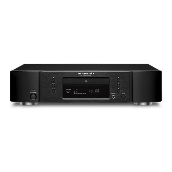
CD PLAYER CD5004
MP3/WMA
DISPLAY
OFF
CD5004
Copyright 2010 D&M Holdings Inc. All rights reserved.
WARNING: Violators will be prosecuted to the maximum extent possible.
CD5004 /
U1B/K1SG/K1B
CD Player
PHONES
LEVEL
-
+
N1B/N1SG
Ver. 1
Advertisement
Table of Contents

Related Manuals for Marantz CD5004


Summary of Contents for Marantz CD5004
- Page 1 Service CD5004 / N1B/N1SG U1B/K1SG/K1B Manual CD Player CD PLAYER CD5004 MP3/WMA STANDBY DISPLAY ON/STANDBY PHONES LEVEL • For purposes of improvement, specifications and design are subject to change without notice. • Please use this service manual with referring to the operating instructions without fail.
- Page 2 MARANTZ Parts for your equipment are generally available to our National Marantz Subsidiary or Agent. ORDERING PARTS : Parts can be ordered either by mail or by Fax.. In both cases, the correct part number has to be specified.
-
Page 3: Safety Precautions
SAFETY PRECAUTIONS The following check should be performed for the continued protection of the customer and service technician. LEAKAGE CURRENT CHECK Before returning the unit to the customer, make sure you make either (1) a leakage current check or (2) a line to chassis resistance check. -
Page 4: Note For Parts List
NOTE FOR SCHEMATIC DIAGRAM WARNING: Parts marked with this symbol z have critical characteristics. Use ONLY replacement parts recommended by the manufacture CAUTION: Before returning the unit to the customer, make sure you make either (1) a leakage current check or (2) a line to chassis resistance check. If the leakage current exceeds 0.5 milliamps, or if the resistance from chassis to either side of the power cord is less than 460 kohms, the unit is defective. -
Page 5: Warning And Laser Safety Instructions
WARNING AND LASER SAFETY INSTRUCTIONS WARNING WAARSCHUWING All ICs and many other semi-conductors are Alle IC’s en vele andere halfgeleiders zijn susceptible to electrostatic discharges (ESD). gevoelig voor elektrostatische ontladingen Careless handling during repair can reduce (ESD). life drastically. Onzorgvuldig behandelen tijdens reparatie When repairing, make sure that you are kan de levensduur drastisch doen connected with the same potential as the... -
Page 6: Technical Specifications
TECHNICAL SPECIFICATIONS n n Audioncharacteristics n n Powernsupply • Channels: 2 channels • Nnversion: AC 230 V 50 Hz • Frequencynresponse: • Unversion: 2 Hz to 20 kHz AC 120 V 60 Hz • Dynamicnrange: 100 dB • Knversion: AC 220 V 50 Hz •... - Page 7 DISASSEMBLY • Disassemble in order of the arrow of the figure of following flow. • In the case of the re-assembling, assemble it in order of the reverse of the following flow. • In the case of the re-assembling, observe "attention of assembling" it. •...
- Page 8 Refer to the table below for a description of the direction in which the photos were taken. • Photographs for which no direction is indicated were taken from above the product. • The photograph is CD5004 K1SG. The viewpoint of each photograph Direction of photograph: B (Photografy direction)
-
Page 9: Front Panel Assy
1. FRONT PANEL ASSY Proceeding : TOP COVER FRONT PANEL ASSY (1) Remove the Loadr Panel. Direction of photograph: B (2) Remove the screws. View from bottom (3) Disconnect the connector wire and FFC Cable. Remove the screws. Cut the wire clamp bands. CN81 FFC Cable Please refer to "EXPLODED VIEW"... - Page 10 2. MAIN PWB Proceeding : TOP COVER MAIN PWB (1) Remove the screws. Direction of photograph: A (2) Remove the screws. Disconnect the connectors wire and FFC Cable. MAIN PWB CN43 CN45 CN42 CN44 Direction of photograph: B FFC Cable CN31...
- Page 11 3. POWER PWB Proceeding : TOP COVER POWER PWB (1) Remove the screws. Direction of photograph: A (2) Remove the screws. Disconnect the connector wires. Cut the wire clamp band. CN94 CN93 CN92 CN91 MAIN PWB CN44 CN45...
- Page 12 4. AUDIO PWB Proceeding : TOP COVER AUDIO PWB (1) Remove the screws. Direction of photograph: A (2) Remove the screws. Disconnect the connector wires. CN81 AUDIO PWB CN43 CN42...
- Page 13 5. MECHA ASSY Proceeding : TOP COVER FRONT PANEL ASSY MECHA ASSY (1) Remove the screws. MECHA ASSY (2) Solder the short-circuit before disconnect the FFC Cable. Short (3) Disconnect the connectors wire and FFC Cable. Cut the wire clamp bands. FFC Cable Direction of photograph: C Connector wire...
-
Page 14: Removing Discs
REMOVING DISCS (1) Remove the Top Cover. (2) Remove the screws. (3) Remove the disc clamper. - Page 15 SERVICE MODE AND TAKING THE DISC OUT OF EMERGENCY [A] SERVICE MODE (1) I nsert mains cable plug in the outlet. (The Unit is standby mode.) (2) P ress the <ON / STANDBY> button While pressing 7 / 9 and 2 Button. Model name is displayed. CD5004 (3) P ress 7 / 9 button. Version of microprocessor is displayed. 2008-05-16-1 (4) P ress 7 / 9 button.
- Page 16 HOW TO THE RESET OF PLAYBACK TIME When replacing CD MECHANISM (TRAVERSE), please reset Playback time (total) in the following procedure. (1) P rocedure 6 of SERVICE MODE, Playback time (total) is displayed. PTime : 00051h The display is a time unit. (Example: "10050 hours, 0 minute, 1 second " is 10051h) The maximum Playback time is 65536h. (2) P ress 2 Button 3 seconds and more. PTime Clear? is displayed. PTime Clear? (3) P ress 1 Button. Done is displayed after PTime:00000h is displayed. Play back time (total) was reset. Done PTime : 00000h Press the <ON / STANDBY> button to quit Service Mode. HOW TO INITIALIZE THE CD PLYAER Initialize the CD player when μcom, peripheral parts of μcom, or MAIN P.W.B. unit has been replaced in servicing.
-
Page 17: About Replace The Microprocessor With A New One
Remark replaced MAIN IC21 T5CD2(F AAD JZ) CD5004 After replaced Mask ROM (With software). No need write-in of software to the microprocessor. Flash ROM (With software). Usually, no need write-in of software. But, when the software was updated, you should be write-in of the new software to the microprocessor or flash ROM. Please check the software version. - Page 18 (3) Double click FlashProg.exe, and launch the Flash Programmer. NOTE : When a Flash Programmer does not launch even if double-clicked FlashProg.exe, please refer to "2. When a Flash Programmer did not launch". (4) Click OK. NOTE : Since Flash Programmer communicates with the unit automatically, the following dialog box appears when it fails in communication.
- Page 19 (5) Click the Setup in the menu bar and select the Object file. (6) Click Browse.
- Page 20 (7) Choose the Motorola S Format(*.s16,*.s24,*.s32) in Files of type. Choose the CD5004_yymmdd_x.s24, and click Open. NOTE : The yy is two digits of year. The mm is month. The dd is date. The x is release number. CD5004_yymmdd_x.s24 CD5004_yymmdd_x.s24 (8) Click Device tab.
- Page 21 (9) Choose the TMP91FW60 in the Device, and choose the 900/L1 in the Series. And click Communication tab. (10) Choose the Serial port number in the COM Port. Check the Data Rate Manual, and choose the 38400 in the Data Rare. And Click OK.
- Page 22 (11) Disconnect the mains cord from the unit. (12) Connect the RS-232C on the connection JIG and the Serial Port of windows PC with RS-232C cable. (13) Connect FFC (upside contact) to the rear panel of the unit from connection JIG. (14) Connect the mains cord into the unit.
- Page 23 (17) Click P (Program) to start update. (18) Software is written into the microprocessor. The writing of software takes about 50 seconds. (19) If the software is updated successfully, a dialog box saying "R006: Programming completed successfully." appears. Click OK.
- Page 24 (20) Click the File in the menu bar and select the Exit. (21) Disconnect mains cord from the unit, and then disconnect FFC of connection JIG from the unit. 2. When a Flash Programmer did not launch (1) Open the FlashProg.ini in the Flash Programmer folder by text editor. (EX.: Notepad, etc)
- Page 25 (2) Delete the text "OpenFile=C:\...(your PC setting)...\???.s24".
- Page 26 (3) Save the FlashProg.ini. (4) Close the text editor. (5) Probably you can launch the Flash Programmer. Go to the 1. Update Procedure step 3.
-
Page 27: Trouble Shooting
TROUBLE SHOOTING 1. POWER PWB N.G. Check FUSE Condition Check the output short of trans ([T901][T902]). [F901]OPEN? If trans is short, trans is replaced. ・FUSE (Open) O.K. Check ST+5V output Check [Q902]corrector input voltage. N.G. ・Voltage Check Check Parts and Soldering and Other Circuits. +5V DC (switched) Voltage is O.K.? If abnormality is not found, [Q902] is replaced. - Page 28 2. FRONT PWB 2.1. FL TUBE dosen't light Check the power supply voltage. POWER PWB N.G. Check the VP (+36V)output. ・[Q901] input +36V DC (switched) Voltage is O.K.? Check Parts and Soldering and Other Circuits. ・[CN21] 19pin If abnormality is not found, [Q901] is replaced. O.K.
- Page 29 3. AUDIO PWB 3.1 No Audio output Check the mute signal (-12V). O.K. Check the analog signal output. AUDIO PWB ・[IC75] 14pin,15pin,18pin,19pin ・[Q603][Q703] base O.K. AUDIO PWB ・[Q605][Q606][Q705][Q706] and Circumference Replace the abnormal IC. N.G. POWER PWB ・[IC94] Check the power supply voltage. N.G.
- Page 30 MEASURING METHOD AND WAVEFORMS Measuring Disc: 4822 397 30184 TCD-784 (It is better to use wires for extending between the probe and test points.) 1. CUP12096Z MCU UNIT: TEST POINT SPIN Tracking RFEQU Focus SLID...
- Page 31 2. WAVEFORMS 1. DISC PLAY RF WAVEFORM(EYE-PATTERN) 2. DISC DETECTION 1.1 CD(TCD-784)Play 2.1 CD(TCD-784)DISC DETECTION 200mV Focus 500Mv Tracking SLID SPIN 2.2 CD-R(TCD-R000RM)DISC DETEC 1.2 CD-R(TCD-R000RM)Play 200mV Focus 500Mv Tracking SLID SPIN 2.3 CD-RW(TCD-W000RM)DISC DETECTION 1.3 CD-RW(TCD-W000RM)Play ...
- Page 32 3. TOC READ 4. FOCUS ADJUSTMENT 3.1 CD(TCD-784)TOC READ 4.1 CD(TCD-784)FOCUS ADJUSTMENT 200mV Focus Tracking 500Mv SLID SPIN 3.2 CD-R(TCD-R000RM)TOC READ 4.2 CD-R(TCD-R000RM)FOCUS ADJUSTMENT 200mV Focus Tracking 500Mv SLID SPIN 3.3 CD-RW(TCD-W000RM)TOC READ 4.3 CD-R(TCD-R000RM)FOCUS ADJUSTMENT 1V 200mV Focus 500Mv Tracking SLID...
-
Page 33: Block Diagram
BLOCK DIAGRAM DSP_MCK UPDATE PORT u-COM SRAM 20Mhz 57 58 59 61 65 67 21 22 33 MEMORY ARRAY OP/SW 256X 1024 TC94A70FG DECODER CD DSP CL/SW SIO/UART 900/L1 CPU A0-A14 DRIVE I.C LIMIT SW (SIO0) High-speed SRAM_WE Oscillator SIO/UART SRAM_OE (SIO1) SRAM_CE... - Page 34 POWER SUPPLY BLOCK DIAGRAM STANDBY TRANS (T902) AC INLET (Q902 U-CON (IC21) IR (RS51) REMOTE IN/OUT MAIN RELAY (RY91) ← STANDBY ON/OFF RELAY (IC77) (IC76) MAIN TRANS +3.3V (T901) (IC94) +12V AUDIO HEAD PHONE -12V RELAY (IC93) (IC92) (IC91) SERVO DRIVE MECHA DRIVE (IC25) (IC33)
- Page 35 WIRING DIAGRAM B TYPE INLET SW41 BK91 BK21 CN22 BK75 JK41 CN23 JK43 JK42 JK71 JK61 BLACK FLASHER PWB (UPDATE PORT) CN41 BN41 CN43 BN43 CORE CORE TRANS BN45 CN45 CN91 AUDIO PWB RELAY MAIN PWB CN44 CN92 CN42 CN21 CN31 CN32 CN33...
- Page 36 PRINTED WIRING BOARDS MAIN (COMPONENT SIDE) 鉛フリー半田 半田付けには、鉛フリー半田 (Sn-Ag-Cu) を使用してください。 Lead-free Solder When soldering, use the Lead-free Solder (Sn-Ag-Cu).
- Page 37 MAIN (FOIL SIDE) 鉛フリー半田 半田付けには、鉛フリー半田 (Sn-Ag-Cu) を使用してください。 Lead-free Solder When soldering, use the Lead-free Solder (Sn-Ag-Cu).
- Page 38 FRONT (COMPONENT SIDE) TACT SW (COMPONENT SIDE) FRONT (FOIL SIDE) TACT SW (FOIL SIDE) 鉛フリー半田 半田付けには、鉛フリー半田 (Sn-Ag-Cu) を使用してください。 Lead-free Solder When soldering, use the Lead-free Solder (Sn-Ag-Cu).
- Page 39 AUDIO (COMPONENT SIDE) AUDIO (FOIL SIDE) 鉛フリー半田 半田付けには、鉛フリー半田 (Sn-Ag-Cu) を使用してください。 Lead-free Solder When soldering, use the Lead-free Solder (Sn-Ag-Cu).
- Page 40 POWER (COMPONENT SIDE) POWER (FOIL SIDE) 鉛フリー半田 半田付けには、鉛フリー半田 (Sn-Ag-Cu) を使用してください。 Lead-free Solder When soldering, use the Lead-free Solder (Sn-Ag-Cu).
- Page 41 HEADPHONE (COMPONENT SIDE) FLASHER (COMPONENT SIDE) FLASHER (FOIL SIDE) TRANSF (COMPONENT SIDE) TRANSF (FOIL SIDE) HEADPHONE (FOIL SIDE) 鉛フリー半田 半田付けには、鉛フリー半田 (Sn-Ag-Cu) を使用してください。 Lead-free Solder When soldering, use the Lead-free Solder (Sn-Ag-Cu).
- Page 42 MAIN PWB CN31 LOADING- R325 LOADING+ TO/FROM C340 CD-OPEN-SW CD MECHANISM 0.1uF HOST HOST ST+5V MGND C341 S_RAM_ADD14 DGND 220u/16V CD-CLOSE-SW IC22 S_RAM_ADD12 SRAM_WE CN23 S_RAM_ADD07 S_RAM_ADD13 IC32 DGND TA2125AF S_RAM_ADD06 S_RAM_ADD08 DGND HOST-RST S_RAM_ADD05 S_RAM_ADD09 C342 DGND DGND DGND 2200P EEPROM_SCL S_RAM_ADD04...
- Page 43 VR81 Q903 FLASHER (IN) PWB AUDIO+ KIA7812API D913 1SS133MT 1N4003 D917 R813 R816 D912 Q802 Q804 AGND SHIELD * ONLY CD5004 U VERSION * KTC3203YT KTA1271YT HDGND HDGND AUDIO- 1N4003 DGND R551 HDGND 47/25V T902 BN44 C804 R820 R824 R828...
- Page 44 EXPLODED VIEW NO. PARTS NO. DESCRIPTION Q'TY A/S PART S4 x1 CTB3+6JR SCREW CTB3+6FFB SCREW CTBD3+8JFB SCREW , DOT S2 x2 CTB3+8JFB SCREW CTW3+8JR SCREW CTW3+8JFZR SCREW S2 x2 CTB3+10JR SCREW S8 x3 CTB3+10JFB SCREW S5 x1 CTW3+12JR SCREW S3 x1 CTW3+18JR SCREW S11 CTB4+6FR...
- Page 45 POWER PWB ASSY COP12097D TACT SW PWB ASSY COP12097B TACT SW PWB ASSY COP12097D TRANSF. PWB ASSY COP12097B TRANSF. PWB ASSY COP12097D 421410006004M MARANTZ BADGE (AL) M1 MODEL CGB1A206 943402009350M TRAY COVER CGR1A455RMWD10 943402009340M TRAY COVER CGR1A455XB37 943416002190M WINDOW FIP CGU1A423A12Z...
- Page 46 Ref. No. Part No. Part Name Remarks Q'ty New 00M32CW107010 SHEET CUSHION FOOT CHG1A360 HOLDER PWB CHE170 HOLDER PWB CHE1A030 BRACKET SUPPORT MECHANISM CMD1A676 943302002290M MECHA LOADER AND TRAVERSE CJDWSL11VF REAR PANEL K CKF3A390T REAR PANEL N CKF3A390V REAR PANEL U CKF4A390W 401310003033M LID TOP COVER SG...
- Page 47 BATTERY CABR03PPB 307010035001M UNIT KIT REMOTE CONTROLLER RC002CD CARTCD5003M 90M-ZD000440R CONN. CORD PIN CJS4M009X 90M-ZD000510R CONN. CORD PIN CJS4N014Z CARD, POST MARANTZ F CQE1A131W SHEET, SALES ADDRESS CQE1A132V STAPLE CPL0905 WARRANTY CARD CQE1A449Z POLY BAG CPB11A008Z 90M-ZC000650R MAINS CORD FOR K...
- Page 48 SEMICONDUCTORS T5CD2 Only major semiconductors are shown, general semiconductors etc. are omitted to list. The semiconductor which described a detailed drawing in a schematic diagram are omitted to list. 1.2 Pin Assignment Diagram 1. IC's T5CD2 (MAIN : IC21) VREFH P30/TB3IN0/INT3/SDA0 AVSS PZ3/R/W AVCC PZ2/HWR P70/TA0IN PZ1/WR...
- Page 49 Terminal Function Pin Power Port Setting Port Name I/O Use Name Note init VREFH VREFH ADC power, connect with +5V AVSS AVCC AVCC MCU power, connect with +5V P70/TA0IN /SRAM_WE sram write enable P71/TA1OUT /SRAM_OE sram output enable P72/TA3OUT /SRAM_CE sram chip enable P73/TA4IN open P74/TA5OUT...
- Page 50 Port Setting Pin Power Port Name I/O Use Name Note init P10/AD8/A8 CD_BUS2 receive data from CD DSP P11/AD9/A9 CD_BUS3 send command to CD DSP P12/AD10/A10 CD_BUCK communication clock with CD DSP P13/AD11/A11 CD_CCE communication chip enable with CD DSP P14/AD12/A12 DSP_RESET CD DSP reset P15/AD13/A13 MT_STBY...
- Page 51 IS61C256AL (MAIN : IC23) TC7WHU04FU (MAIN : IC26)
- Page 52 CDCE913 CDCEL913 www.ti.com CDCE913PWR (MAIN: IC27) SCAS849B – JUNE 2007 – REVISED DECEMBER 2007 Programmable 1-PLL VCXO Clock Synthesizer With 1.8-V, 2.5-V, and 3.3-V Outputs FEATURES • Flexible Clock Driver • Member of Programmable Clock Generator – Three User-Definable Control Inputs 2345 CDCE913 Family [S0/S1/S2], for example., SSC Selection,...
- Page 53 TC94A70FG/TC94A73MFG TC94A70FG Single-chip CD-MP3 Processor Pin description (top view) TC94A70FG (MAIN : IC31) Description engineering investment needed to upgrade TC94A70FG CD playback designs with ESP. TC94A70FG and TC94A73MFG are highly egrated solution New product design is further aided by integrated, high-performance CD-MP3 servo, RF amp, programmable RAM and macro commands LPFo Pio2 solutions that enable playback of CD and...
- Page 54 TC94A70FG TC94A70FG 1. Pin Descriptions Terminal Function Symbol Description Default Remarks Symbol Description Default Remarks AVSS3 - Grounding pin for 3.3V CD analog circuits. - DVSS3 - Grounding pin for 3.3V DAC circuit - Connect to RFRP by RFZi Input pin for RF ripple zero-cross signal. R channel audio output pin of Audio DAC.
- Page 55 5 V regulator reference amp (with external output Tr.) · Thermal shut down protection · Operating supply voltage range: V = 5.0-9.0 V · Block Diagram TA2125AF (MAIN : IC32) Block Diagram Driver RIN FIN STB IN3 IN4 REG OUT N.C. ´ 3 ´ 3 ´...
- Page 56 TC74HCU04AFNG (FRONT: IC51)
- Page 57 D/A, Output Analog Filtering digital-to-analog conversion, digital de-emphasis, vol- 114 dB Dynamic Range ume control, channel mixing and analog filtering. The 100 dB THD+N advantages of this architecture include: ideal differential CS4392 Up to 192kHz Sample Rates linearity, no distortion mechanisms due to resistor matching errors, no linearity drift over time and tempera- Direct Stream Digital Mode CS4392KZZ (AUDIO: IC75)
- Page 58 PARTS LIST OF P.W.B. UNIT * Parts for which "nsp" is indicated on this table cannot be supplied. * The parts listed below are for maintenance only, might differ from the parts used in the unit in appearances or dimensions. Note: The symbols in the column "Remarks"...
- Page 59 Ref. No. Part No. Part Name Remarks Q'ty New C754 00MOA10701620 ELECT CAP100UF 16V CCEA1CH101T C755 00MOA22605020 ELECT CAP22UF 50V CCEA1HH220T C756 CER. CAP0.1UF 50V Z CERAMIC CCBS1H104ZFT C757 00MOA22605020 ELECT CAP22UF 50V CCEA1HH220T C758 00MOA47602520 ELECT CAP47UF 25V CCEA1EH470T C759 CER.
- Page 60 FRONT PWB (CUP12097Z-1) Ref. No. Part No. Part Name Remarks Q'ty New SEMICONDUCTORS GROUP IC51 90M-HC700550R IC TC74HCU04AFNG HVI74HCU04AFNG Q502 90M-BA001460R TRS KRC107M HVTKRC107MT Q503 90M BA001460R TRS KRC107M HVTKRC107MT D502 90M-HI101120R L.E.D SLR325VRA47 KVDSLR325VRA47 D503 90M-HI101120R L.E.D SLR325VRA47 KVDSLR325VRA47 FL51 90M-HQ300610R FL DISPLAY FOR CD5400...
- Page 61 HEADPHONE PWB (CUP12097Z-4) Ref. No. Part No. Part Name Remarks Q'ty New SEMICONDUCTORS GROUP IC81 00MHC10102090 IC NJM2068M HVINJM2068MTE1 Q801 00MHT800951B0 TRS KTC3203Y HVTKTC3203YT Q802 00MHT800951B0 TRS KTC3203Y HVTKTC3203YT Q803 00MHT600141B0 TRS KTA1271Y HVTKTA1271YT Q804 00MHT600141B0 TRS KTA1271Y HVTKTA1271YT Q807 00MHT805501B0 TRS KTC2874B HVTKTC2874BT Q808...
- Page 62 MAIN PWB (CUP12096Z) Ref. No. Part No. Part Name Remarks Q'ty New SEMICONDUCTORS GROUP IC21 943243002430M U-PROT5CD2(F AAD JZ) MAIN CPU CD5003 CVIT5CD2 IC22 90M-HC109780R IC AT24C02NSU EEPROM(2K) CVIAT24C02NSU18 IC23 943246002440S IC IS61C256AL-12JLI CVIS61C256AL12J IC24 00MHC10099540 IC S-80145ALMC HVIS-80145ALMC IC25 943231002450S IC KIA1117S18-RTK/ CVIKIA1117S18...
- Page 63 Ref. No. Part No. Part Name Remarks Q'ty New C301 00MDK96104300 CER. CAP.0.1UF 50V K CCUS1H104KC C306 00MDK96104300 CER. CAP.0.1UF 50V K CCUS1H104KC C310 00MDD95470300 CER. CAP.47PF 50V JA CCUS1H470JA C311 00MDK96333300 CER. CAP.0.033UF 50V K CCUS1H333KC C312 00MDK96104300 CER. CAP.0.1UF 50V K CCUS1H104KC C313 00MOA47602520 ELECT CAP.47UF 25V...
- Page 64 Ref. No. Part No. Part Name Remarks Q'ty New C465 00MDK96104300 CER. CAP.0.1UF 50V K CCUS1H104KC C466 00MOA10701620 ELECT CAP.100UF 16V CCEA1CH101T C467 00MOA10701620 ELECT CAP.100UF 16V CCEA1CH101T C468 00MDK96104300 CER. CAP.0.1UF 50V K CCUS1H104KC C990 00MDK96104300 CER. CAP.0.1UF 50V K CCUS1H104KC C991 00MDK96104300...
- Page 65 POWER PWB (CUP12097Z-3) Ref. No. Part No. Part Name Remarks Q'ty New SEMICONDUCTORS GROUP IC91 90M-HC300780R IC KIA7808API HVIKIA7808API IC92 00MHC3890599F IC KIA7805API HVIKIA7805API IC93 00MHC3991209F IC KIA7912PI HVIKIA7912PI IC94 00MHC3891299F IC KIA7812API HVIKIA7812API Q901 90M-HT800040R TRS KSC2316Y HVTKSC2316YT Q902 90M-HT800040R TRS KSC2316Y HVTKSC2316YT...
- Page 66 Ref. No. Part No. Part Name Remarks Q'ty New CN93 CONN 7P STRAIGHT 20017WS-07 CJP07GA19ZY CN94 CONN 3P STRAIGHT YMW025-03R CJP03GA01ZY z F901 90M-FS001260R FUSE T 315MA L 250V KBA2C0315TLEY z F901 90M-FS001370R FUSE 250V T 0.63A KBA2C0630TLEY HF91 CONN HOLDER FUSE KJCFC5S HF92 CONN HOLDER FUSE...
- Page 67 FLASHER IN PWB (CUP12097Z 6) Ref. No. Part No. Part Name Remarks Q'ty New SEMICONDUCTORS GROUP Q551 00MBA10001000 TRS KRA102M HVTKRA102MT D551 00MHD20015210 DIODE 1SS133T-77 CVD1SS133MT D552 90M-HI200020R L.E.DSIR-34ST3F BVDSIR34ST3F D553 00MHD20015210 DIODE 1SS133T-77 CVD1SS133MT CAPACITORS GROUP C551 00MOA10701620 ELECT CAP100UF 16V CCEA1CH101T C552 CER.
- Page 68 Personal notes:...