Table of Contents
Advertisement
SERVICE MANUAL
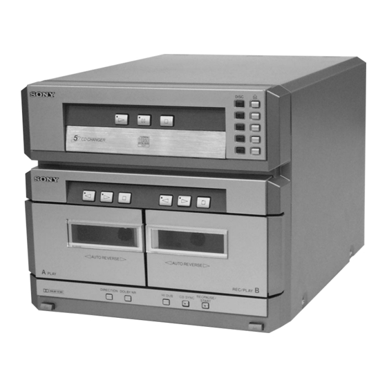
Htc-Nx1 is the CD player and Tape
Deck section in MHC-NX1/NX3AV.
Dolby noise reduction manufactured under license
from Dolby Laboratories Licensing Corporation.
"DOLBY" and the double-D symbol a are trade-
marks of Dolby Laboratories Licensing Corporation.
MICROFILM
HTC-NX1
Model Name Using Similar Mechanism
CD Mechanism Type
CD
Section
Base Unit Name Type
Optical Pick-up Name
Model Name Using Similar Mechanism
Tape Deck
Section
Tape Transport Mechanism Type
SPECIFICATIONS
MINI Hi-Fi COMPONENT SYSTEM
US Model
Canadian Model
AEP Model
UK Model
E Model
Australian Model
Tourist Model
HCD-MD555
CDM53D-K1BD33
BU-K1BD33
KSM-213BFN-C2NP
HCD-GRX7
TCM-230AWR2
Advertisement
Table of Contents

Related Manuals for Sony HTC-NX1


Summary of Contents for Sony HTC-NX1
- Page 1 Canadian Model AEP Model UK Model E Model Australian Model Tourist Model HTC-NX1 is the CD player and Tape Deck section in MHC-NX1/NX3AV. Dolby noise reduction manufactured under license Model Name Using Similar Mechanism HCD-MD555 from Dolby Laboratories Licensing Corporation.
- Page 2 HTC-NX1 7-3. SCHEMATIC DIAGRAM – BD Board – • See page 32 for Waveforms. • See page 32 for IC Block Diagrams. (Page 29) • Voltages and waveforms are dc with respect to ground under no-signal conditions. no mark : CD PLAY The components identified by mark 0 or dotted Les composants identifiés par une marque 0 sont...
- Page 3 HTC-NX1 • Voltages are dc with respect to ground under no-signal conditions. no mark : CD PLAY 7-5. SCHEMATIC DIAGRAM – CD MOTOR/SENSOR Section – • See page 33 for IC Block Diagram. (Page 29) (Page 29)
- Page 4 HTC-NX1 7-7. SCHEMATIC DIAGRAM – AUDIO Board – • See page 33 for IC Block Diagram. PB EQ AMP (PLAYBACK) (DECK A) PB LEVEL (L) (DECK A) PB LEVEL (R) (DECK A) PB EQ AMP (DECK B) PB LEVEL (L) (DECK B) A +7.5V...
- Page 5 HTC-NX1 7-8. PRINTED WIRING BOARD – LEAF SW Board – • See page 19 for Circuit Boards Location. DECK B DECK A PLUNGER PLUNGER (DECK B PLAY) (DECK B 120/70) (DECK A PLAY) (DECK B HALF) (DECK A REC) (DECK A 120/70)
- Page 6 HTC-NX1 7-11. SCHEMATIC DIAGRAM – MAIN Board (1/2) – (Page 25) (Page 26) (Page 29) • Voltages are dc with respect to ground under no-signal conditions. no mark : CD PLAY The components identified by mark 0 or dotted Les composants identifiés par une marque 0 sont ) : TAPE PLAYBACK (DECK A) line with mark 0 are critical for safety.
- Page 7 HTC-NX1 7-12. SCHEMATIC DIAGRAM – MAIN Board (2/2) – • See page 32 for Waveform. (Page 28) (Page 31) (Page 23) (Page 23) (Page 31) (Page 31) (Page 21) • Voltages and waveforms are dc with respect to ground ] : TAPE PLAYBACK (DECK B) 〈〈...
- Page 8 HTC-NX1 7-14. SCHEMATIC DIAGRAM – PANEL Section – (Page 29) (Page 29) (Page 29) • Voltages are dc with respect to ground under no-signal conditions. no mark : CD PLAY...
- Page 9 • Waveforms • IC Block Diagrams – BD Board – – MAIN Board – – BD Board – IC101 CXD2587Q 5 IC101 yh (XTAI) 1 IC101 qd (XOUT) 1 IC103 qh (RF O) (CD Play Mode) Approx. 3 Vp-p 1.9 Vp-p 1.2 Vp-p ERROR DIGITAL...
- Page 10 IC103 CXA2568M-T6 HOLD APC PD AMP LC/PD APC LD AMP – LD ON – – – HOLD SW AGC CONT AGC VTH 50µA RF BOT – – – – RFTC RF SUMMING AMP RF EQ AMP RF I RF O –...