Chapters
Table of Contents

Related Manuals for Panasonic DMR-ES40VP


Summary of Contents for Panasonic DMR-ES40VP
-
Page 1: Dvd Video Recorder
ORDER NO.VR0508007CE DVD Video Recorder DMR-ES40VP DMR-ES40VPC Vol.1 Colour (S).......Silver Type © 2005 Matsushita Electric Industrial Co., Ltd. All rights reserved. Unauthorized copying and distribu- tion is a violation of law. -
Page 2: Table Of Contents
TABLE OF CONTENTS PAGE PAGE 1 Safety Precaution -------------------------------------------------3 1.1. General guidelines -----------------------------------------3 1.2. Caution for fuse replacement ---------------------------3 2 Warning --------------------------------------------------------------4 2.1. Prevention of Electrostatic Discharge (ESD) to Electrostatic Sensitive (ES) Devices ---------------4 2.2. Precaution of Laser Diode -------------------------------5 2.3. -
Page 3: Safety Precaution
1 Safety Precaution 1.1. General guidelines 1. When servicing, observe the original lead dress. If a short circuit is found, replace all parts which have been overheated or damaged by the short circuit. 2. After servicing, see to it that all the protective devices such as insulation barriers, insulation papers shields are properly installed. -
Page 4: Warning
2 Warning 2.1. Prevention of Electrostatic Discharge (ESD) to Electrostatic Sensitive (ES) Devices Some semiconductor (solid state) devices can be damaged easily by static electricity. Such components commonly are called Elec- trostatic Sensitive (ES) Devices. Examples of typical ES devices are integrated circuits and some field-effect transistor-sand semi- conductor "chip"... -
Page 5: Precaution Of Laser Diode
2.2. Precaution of Laser Diode 2.3. Handling the Lead-free Solder 2.3.1. About lead free solder (PbF) Distinction of PbF P.C.B.: P.C.B.s (manufactured) using lead free solder will have a PbF stamp on the P.C.B. Caution: • Pb free solder has a higher melting point than standard solder; Typically the melting point is 50 - 70°F (30 - 40°C) higher. Please use a high temperature soldering iron. -
Page 6: Service Navigation
3 Service Navigation 3.1. Service Information 3.2. (DVD) Service Navigation 3.2.1. Flow chart for contirmation... - Page 7 3.2.2. Confirm “RAM-Drive Last Error” in Service Mode Execute Service Mode 1. Press [VHS to DVD DUBBING], [OPEN/CLOSE] and [STOP] keys simultaneously for 5 seconds when P-off. FL Display: *After finishing display “(9). Factor of Drive Error occurring”, press [0] [2] ~[9] [9] keys of the Remote Controller so that 99 memories can be displayed as maximum.
- Page 8 (5) Last Drive Error code No2. (1/2) is displayed for 5 seconds. (6) Last Drive Error code No2. (2/2) is displayed for 5 seconds. (7) Error occurring Disc type is displayed for 5 seconds. (8) Unused (No display). (9) Factor of Drive Error occurring is left displayed Error Occurring Disc State...
-
Page 9: Specifications
4 Specifications... -
Page 10: Features
5 Features 5.1. Quick start function (REC) 1. General A few seconds after tuning on the unit,you can start recording to DVD-RAM. You can switch the operation of this function (ON/OFF) on the menu screen. 2. Quick start(REC) principle In the power-off at Quick start, only power supplies for video IC,tuner and storage media are cut off. When the REC button is pushed a few second after the power button is pushed, Audio and Video data are stored in DDR SDRAM before a storage media (DVD-RAM) preparation. -
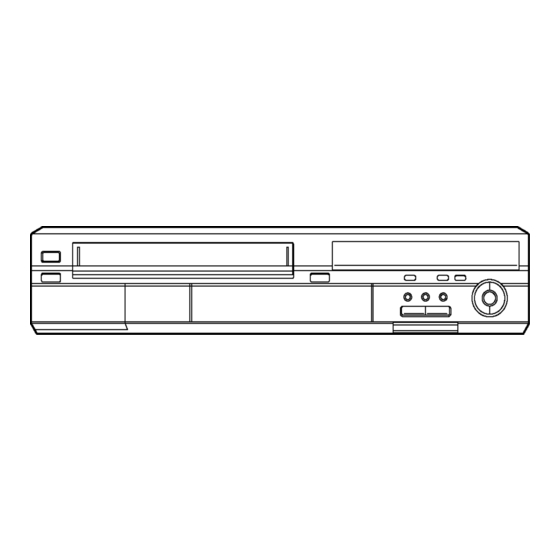
Page 11: Location Of Controls And Components
6 Location of Controls and Components 6.1. Each Buttons... -
Page 13: Operation Instructions
7 Operation Instructions 7.1. (DVD) Taking out the Disc from RAM-Drive Unit when the Disc cannot be ejected by OPEN/CLOSE button 7.1.1. (DVD) Forcible Disc Eject 7.1.1.1. (DVD) When the power can be turned off. 1. Turn off the power and press [STOP], [CH UP] keys on the front panel simultaneously for 5 seconds. 7.1.1.2. -
Page 14: Vhs) Removing Cassette Tape Manually
7.2. (VHS) Removing Cassette Tape 3. Stop unloading just before unloading will be completed as shown below, and then the tape becomes slack as shown manually below. When the cassette tape could not be uninstalled from an elec- 4. Rotate the S-Reel by a small minus screwdriver to trical malfunction, there are 2 ways to remove a cassette tape. - Page 15 7.2.3. (VHS) Take out Cassette Tapeman- 6. Attach Loading Motor and tighten the screw. 7. Set the Position Switch to EJECT POSITION certainly ually after removing the mecha- and attach the mechanism to chassis as shown below. nism 1. Disconnect the AC plug, and remove the Top Panel, Front Panel and the Mechanism by referring to "14 Assem- bling and Disassembling"...
-
Page 16: Service Mode
8 Service Mode 8.1. (DVD) Self-Diagnosis and Special Mode Setting 8.1.1. (DVD) Self-Diagnosis Functions Self-Diagnosis Function provides information for errors to service personnel by “Self-Diagnosis Display” when any error has occurred. U**, H** and F** are stored in memory and held. Display on FL will be cancelled when the power is turned off or AC input is turned off during self-diagnosis display is ON. - Page 17 Error Code Diagnosis contents Description Monitor Display Automatic FL display PLEASE Unit is in termination process Unit is in termination process now. No display WAIT “BYE” is displayed and power will be turned off. In case “Quick Start” of setup menu is ON, it is displayed in restoration operation for AC off.
- Page 18 Item FL display Key operation Mode name Description Front Key Aging Contents (Example): Demonstration lock/ Ejection of the disc is prohibited. *When lock the tray. When the power is on, press unlock The lock setting is effective until unlocking the [STOP] and [POWER] keys simulta- tray and not released by “Main unit initializa- neously for 5 seconds.
- Page 19 8.1.3. (DVD) Service Modes at a glance Service mode setting: While the power is off, press [STOP], [VHS to DVD DUBBING] and [OPEN / CLOSE] simultaneously for five seconds (OPERATION SELECT should be set to DVD). Item FL display Key operation Mode name Description (Remote controller key)
- Page 20 Item FL display Key operation Mode name Description (Remote controller key) RTSC Return in XP L1 input signal is encoded (XP), decoded Initial mode: EE2/ Interlace/ XP/ Press [1] [3] in service mode. (A & V) (XP) and output decoded signal to external Audio 48kHz without DISC recording and DISC playback.
- Page 21 Item FL display Key operation Mode name Description (Remote controller key) RAM Drive Last Error RAM Drive error code display. 1. Error Number is displayed for 5 Press [4] [2] in service mode. *For details about the drive error code, refer seconds.
- Page 22 Item FL display Key operation Mode name Description (Remote controller key) S1 signal output Forcibly superimpose the S1 signal (approx. Press [5] [2] in service mode. 4.5V DC) on the EE chroma signal, and check the output on the S terminal. S2 signal output Forcibly superimpose the S2 signal (approx.
-
Page 23: Vhs) Self-Diagnosis And Special Mode Setting
8.2. (VHS) Self-Diagnosis and Special Mode Setting 8.2.1. (VHS) Self-Diagnosis Functions This model has a self-diagnosis and display function. If the VHS section detects trouble during installation or during use, one of the following Error Codes will automatically appear in the display on VHS side. Error Codes are displayed in the form of a single English letter followed by two numbers, as for example "H01". - Page 24 8.2.2. (VHS) Special Modes Setting Item FL display Key operation Mode name Description Front Key Tracking Center Tape Tracking is adjusted to center No display. During PLAYBACK, press [(VHS) CH FIX position. UP] and [(VHS) CH DOWN] keys simultaneously. VHS Service Mode In order to make service easy, a part Press [FF], and [EJECT] keys simul- of inside information of a micropro-...
- Page 25 Service Contents Contents of Indication on minute Contents of Indication on second Remarks Number Indication for the Mechanism position Ordering for the Motors There are next conditions in this inner data (Real time) (Real time) mode for enable the mechanism IC6001 0L: EJECT position 0*, 2*: CYL off,...
- Page 26 8.2.4.2. (VHS) Condition for clearing the self-diagnosis history 1. A case of that press the FF key and the EJECT key simultaneously over 5 seconds. 2. A case of that the factory jumper (TW1004) is shorted. 8.2.4.3. (VHS) Indication of the self-diagnosis history. 1.
- Page 27 <Supplementary Data 4> (LM Information) Result of request of driving Loading Motor. Display Description There was no change of mechanism position. (Loading Motor was OFF) There was some change of mechanism position. (Loading Motor was ON) 8.2.5. (VHS) Description of Self Diagnosis Memory In this Self-Diagnosis Function, in case error has occurred continuously, maximum of the newest 3 error data are memorized.
- Page 28 Note 1: Details of "VHS mode" of the Supplementary Data 1 (These values are hexadecimal indication) 0: STOP, 1: EJECT, 2: REW, 3: FF, 4:REV, 5: CUE, 6: SLOW, 7: POWEROFF, 8: PLAY, 9: STIL, A: REC, B: REC PAUSE, C: ADUB, D: ADUB PAUSE, E: INSERT, F: INSERT PAUSE Note 2: Explanation of "Tape position"...
-
Page 29: Service Fixture & Tools
9 Service Fixture & Tools (For DVD) Part Number Description Compatibility RFKZ0125 Extension FFC (Power & Digital I/F P.C.B. - DVD-RAM Drive / 40 Pin) Same as DMR-E50 / E55 / ES10 / ES30V series RFKZ0168 Extension Cable (Power & Digital I/F P.C.B. - FAN / 3 Pin) Same as DMR-E50 / ES30V series RFKZ0126... -
Page 30: Disassembly And Assembly Instructions
10 Disassembly and Assembly Instructions 10.1. Disassembly Flow Chart The following chart is the procedure for disassembling the casing and inside parts for internal inspection when carrying out the ser- vicing. To assemble the unit, reverse the steps shown in the chart below. -
Page 31: Positions
10.2. P.C.B. Positions 10.3. Caution with inserting cassette tape when disassembling the unit Note1: For description of the disassembling procedure, see the section 11.4. Note2: Video Cassette might not enter when a strong lighting is applied to VHS Mechanism when Video Cassette is inserted. Please weaken the lighting or cover with the top panel etc. -
Page 32: Top Case
10.4. Top Case 10.5. Front Panel 1. Remove the 4 screws (A) and 3 screws (B). 1. Remove one screw (A). 2. Slide Top Case rearward and open the both ends at rear 2. Unlock tab (A) and tab (B) simultaneously. side of the Top Case a little and lift the Top Case in the 3. -
Page 33: Front Jack P.c.b. & Front P.c.b
10.7. Rear Panel with Fan Motor Note: When attaching Front Panel, in order to hook Cassette Door 1. Disconnect Fan Connector. Opener Lever to Cassette Door, push up cassette door in 2. Remove 5 Screws (A) and 1 Screw (B). the direction of arrow and insert a front panel. -
Page 34: Vtr Mechanism Unit
10.8. VTR Mechanism Unit 10.8.1. Caution for attaching VTR Mecha- nism Unit 1. Disconnect 3 Connectors (P1531, P2501 and P4002). 2. Remove 3 Black Screws (A), Screw (B) , Screw (C) and 1. Because Position SW should be set to "Eject Position", Screw (D). -
Page 35: Main P.c.b
10.9. Main P.C.B. 10.10. DVD-RAM Drive 1. Disconnect 3 Connectors. 1. Remove 3 Screws (A). 2. Remove 1 Screw (A) and remove Main P.C.B. 2. Lift up DVD-RAM Drive slightly. 3. Disconnect Connector (A) and FFC from DVD-RAM Drive. -
Page 36: Digital P.c.b
10.11. Digital P.C.B. 10.11.1. Removing and attaching Heat Sink Unit for IC5001 1. Remove 3 Screws (A). 2. Disconnect connector (A) and FFC from Digital P.C.B.. 3. Lift up Digital P.C.B. slightly so to disconnect connector (B) to remove Digital P.C.B.. CAUTION: When replacing Digital P.C.B., pay attention to inserting FFC. -
Page 37: Dv Jack P.c.b
10.12. DV Jack P.C.B. 10.13. Power & Digital I/F P.C.B. 1. Remove 4 Screws (A) and DVD Angle. 1. Remove 3 Screws (A) and DV Jack Angle. 2. Remove Fan Motor (refer to 11.7.1.). 3. Disconnect 3 Connectors (A) and 2 Connectors (B). 4. -
Page 38: Measurements And Adjustments
11 Measurements and Adjustments 11.1. Service Positions Note: For description of the disassembling procedure, see the section 10. 11.1.1. Checking and Repairing of Power & Digital I/F P.C.B. - Page 39 11.1.2. Checking and Repairing of Main P.C.B.
- Page 40 Checking and Repairing of Digital P.C.B. 11.1.3.
- Page 41 Checking and DVD-RAM Drive 11.1.4.
-
Page 42: Dvd) Caution After Parts Replacing Parts
11.2. (DVD) Caution after parts replacing parts 11.2.1. (DVD) After replacing the RAM Drive with new one 11.2.2. (DVD) When the unit does not operate normally after replacing the Timer Micropro- cessor or Main P.C.B. When the unit does not operate normally after replacing the Timer Microprocessor or Main P.C.B. with new one, reset Timer Micro- processor. -
Page 43: Vhs) Caution After Replacing Parts
11.3. (VHS) Caution after replacing parts PG Shifter Automatic Adjustment and X-VALUE & LINEARITY (P2 and P3 Posts) ADJUSTMENT should be performed after replacing DD Cylinder, Timer Microprocessor or Main P.C.B. Note: The “X-VALUE & LINEARITY (P2 and P3 Posts) ADJUSTMENT” is not necessary after only replacement of Timer Microproces- sor or Main P.C.B. - Page 44 11.3.2. (VHS) X-VALUE & LINEARITY (P2 and P3 Posts) ADJUSTMENT l Main symptoms and Adjustment point Envelope Post Name Adjustment Method P2 Post Turn P2 Post counter-clockwise (Approx. 1/2 revolution) P2 Post Turn P2 Post clockwise (Approx. 1/4 revolution) P3 Post Turn P3 Post clockwise (Approx.
-
Page 45: Dvd) Standard Inspection Specifications After Making Repairs
Turn on the power, and confirm items pointed out. Items pointed out should reappear. Insert RAM disc. The Panasonic RAM disc should be recognized. Enter the EE (TU IN / AV IN - AV OUT) mode. No abnormality should be seen in the picture, sound or operation. -
Page 46: Miscellaneous
12 Miscellaneous INITIAL/LOGO ABBREVIATIONS ERROR TORQUE CONTROL 12.1. Abbreviations ERROR TORQUE CONTROL REFER- ENCE 12.1.1. DVD ENCSEL ENCODER SELECT ETMCLK EXTERNAL M CLOCK (81MHz/40.5MHz) ETSCLK EXTERNAL S CLOCK (54MHz) INITIAL/LOGO ABBREVIATIONS FBAL FOCUS BALANCE A0~UP ADDRESS FCLK FRAME CLOCK ACLK AUDIO CLOCK FOCUS ERROR AD0~UP... - Page 47 INITIAL/LOGO ABBREVIATIONS INITIAL/LOGO ABBREVIATIONS READ ENABLE VBLANK V BLANKING RFENV RF ENVELOPE COLLECTOR POWER SUPPLY RF PHASE DIFFERENCE OUTPUT VOLTAGE (CD-ROM) REGISTER SELECT VCDCONT VIDEO CD CONTROL (TRACKING RSEL RF POLARITY SELECT BALANCE) RESET DRAIN POWER SUPPLY VOLTAGE RESERVE VIDEO FEED BACK VREF VOLTAGE REFERENCE SBI0, 1...
- Page 48 12.1.2. VHS 3-1. ABBREVIATIONS 4.43 NTSC L 443NT [L] BILINGUAL BILINGUAL L A. COMP BIL [L] AUDIO COMPONENT SIGNAL BILINGUAL H BIL. [H] A. COMPO AUDIO COMPONENT SIGNAL AUDIO DUBBING PAUSE L BILINGUAL L BIL/M1 [L] A. D.P [L] AUDIO DUBBING PAUSE L BS CLOCK A.
- Page 49 CYL GND CYLINDER GND FULL. E. 12V FULL ERASE 12V DELAIED FM RECORDING H D.F.M. REC [H] GND [A] GND (ANALOG) DELAIED FM RECORDING L D. FM REC [L] GND [TU] GND (TUNER) D. GND DIGITAL GND GND/N. SW. 12V GND/NON SW 12V DELAYED RECORDING H D.
- Page 50 POWER OFF H LINE IN [R] LINE INPUT (R) P-OFF [H] POWER OFF L LINE OUT [L] LINE OUTPUT (L) P-OFF [L] LINE OUT [R] LINE OUTPUT (R) P. FAIL POWER FAILURE DETECT LP H POWER OFF H LP [H] P.
- Page 51 RF OUT RF OUTPUT SYSCON 5V SYSTEM CONTROL 5V RF Y RF LUMINANCE SIGNAL SYSTEM SYSTEM SW RF. Y. IN RF LUMINANCE SIGNAL INPUT T-PHOTO TAKE-UP PHOTO TRANSISTOR TAKE-UP REEL PULSE RF. Y. OUT RF LUMINANCE SIGNAL OUTPUT T-RL. PLS TIMER BUS CLOCK ROTAR.
- Page 52 DVD Video Recorder when there is no specify mode is mentioned. DMR-ES40VP 4.Although the voltage and waveform available on here is measured with standard frame, it may be differ from actual measurement due to modification of circuit and so on.
-
Page 53: S2. Voltage And Waveform Chart
S2. Voltage and Waveform Chart S2.1. Main P.C.B. <IC3001> REF No. PIN No. REC REF No. PIN No. REC REF No. PIN No. REC REF No. PIN No. REC REF No. PIN No. REC REF No. PIN No. REC IC3001 IC3001 IC3701 IC4501... - Page 54 REF No. PIN No. REC REF No. PIN No. REC REF No. PIN No. REC REF No. PIN No. REC REF No. PIN No. REC IC6001 IC7301 IC7501 Q3004 QR4807 IC6001 IC7301 IC7501 Q3004 QR4810 IC6001 IC7301 IC7501 Q3004 QR4810 IC6001 IC7301 IC7501...
-
Page 55: S2.2. Power And Digital I/F P.c.b
S2.2. Power and Digital I/F P.C.B. <IC11201> <IC11202> REF No. PIN No. REC REF No. PIN No. REC REF No. PIN No. REC REF No. PIN No. REC IC45002 P37101 QR11402 IC11201 IC45002 P37101 QR11501 IC11201 IC45002 P37101 QR11501 IC11201 IC45002 P37101 QR11501... -
Page 56: S3. Power Supply Block
(SWITCHING IC) P31903 P6003 MAIN P.C.B. DP7501- DRAIN 5 IP11902 X SW-7V D11206 D11207 X SW+4V Q11302 (FEED BACK) X SW+3.2V DIGITAL I/F SECTION IC11302 X SW+5.8V (ERROR VOLTAGE DET.) X SW+12V IP11903 X SW+36V COLD DMR-ES40VP/PC Power Supply Block Diagram... -
Page 57: S3.2. Digital I/F Regulator Block Diagram
P31901 P6001 D +1.8V P31901 P6001 82,84,86,88 IC11501 (DC-DC CONVERTER) DIGITAL P.C.B. V IN IC31004 (REG.ANA +3.3V) ON/OFF QR11501,11502 8 CS ANA +3.3V P37101 P6001 (POWER ON OUT) V IN V OUT 1 38,42 DMR-ES40VP/PC Digital I/F Regulator Block Diagram... -
Page 58: S3.3. Video Block Diagram(1
CPN Y IN1 V YIN DM P6002 P31902 P37101 P6001 CLAMP P.C.B. S-VIDEO IN C/S DET1 L1 CS DET V-SW B SW B Y/V OUT B MIX V OUT MIX B Y-SW B MIX B C-SW B DMR-ES40VP/PC Video Block Diagram... -
Page 59: S3.4. Video Block Diagram(2
SQPB SQPB P3001 629MHz P-EQ EP L TRAP TO/FROM AUDIO SECTION P3001 2FSC EP COM DD CYLINDER SQPB VIDEO HEAD IC4501- P3001 EP R C CLOCK TO C CCD DRIVER SYSTEM CONTROL SECTION Q3001 BUFFER IC6001- DMR-ES40VP/PC Video Block Diagram... -
Page 60: S3.5. Audio Block Diagram
MIX R OUT DM P31902 P6002 JK4801 DIGITAL AUDIO OUT FROM MIX L OUT DM DVD L OUT P6001 P37101 MIX L OUT DM P31902 P6002 DIGITAL P.C.B. PCM/ BITSTREAM P6001 P37101 P31901 P6001 IECOUT IEC OUT DMR-ES40VP/PC Audio Block Diagram... -
Page 61: S3.6. System Control And Servo Block Diagram
IC1512 (T-REEL SENSOR) (S-REEL SENSOR) IIC CLOCK 71 IIC CLOCK TO/FROM VIDEO IC(IC3001)/ TL24 AUDIO IC(IC4501) IIC DATA IIC DATA 79 S.REEL TL23 DMR-ES40VP/PC Q1501 D1501 Q1502 S1531 System Control & Servo TAKE-UP SENSOR SUPPLY SAFETY PHOTO PHOTO TAB SW 80 T.REEL... -
Page 62: S3.7. Timer Block Diagram
60 TBUS CLK P.C.B. IC6001 (SYSTEM CONTROL/SERVO/TIMER) P7502 PP27501 LED3 QR27501 DUB RED (DUBBING LED DRIVE) D27501 P7502 PP27501 LED1 QR27503 (DVD LED DRIVE) D27503 AD +5V P7502 PP27501 LED2 QR27505 (VHS LED DRIVE) D27505 DMR-ES40VP/PC Timer Block Diagram S-11... -
Page 63: S4. Schematic Diagram
S4. Schematic Diagram S4.1. Interconnection Diagram DMR-ES40VP/PC Interconnectin Schematic Diagram MAIN PCB VJB06F99 P6001 P31901 K1KB15AA0032 K1KA15A00118 MUTE_L MUTE_L SYNC_DET SYNC_DET X_SW5R8V X_SW5R8V X_SW5R8V X_SW5R8V X_SW12V X_SW12V X_SW12V X_SW12V IECOUT IECOUT DR_P_ON_H DR_P_ON_H I2C5_CK I2C5_CK I2C5_DT I2C5_DT SCURVE0 SCURVE0 SCURVE1... - Page 64 DMR-ES40VP/PC Interconnectin Schematic Diagram DRIVE PCB VJB72106 P6001 P31901 K1KB15AA0032 K1KA15A00118 MUTE_L MUTE_L SYNC_DET SYNC_DET X_SW5R8V X_SW5R8V X_SW5R8V X_SW5R8V X_SW12V X_SW12V D_I/F PCB X_SW12V X_SW12V VJB09138 IECOUT IECOUT DR_P_ON_H DR_P_ON_H I2C5_CK I2C5_CK I2C5_DT I2C5_DT SCURVE0 SCURVE0 SCURVE1 SCURVE1 P31902 P6002...
- Page 65 P_OFF_L X_SW36V XINTP XINTP SCLK SCLK XINTM XINTM SBPTM SBPTM SBMTP SBPTP XMPREQ XMPREQ LOADING M XTMUTE_L XTMUTE_L IF OUT SYS_PFAIL SYS_PFAIL AFTOUT [US] AUDIOOUT SIFOUT BTL+30VIN VIDEOOUT FRONT JACK PCB FRONT PCB VJB04888 VJB07A85 DMR-ES40VP/PC Interconnectin Schematic Diagram S-14...
- Page 66 D3R3V DGND DGND D3R3V DGND DGND DGND DGND SYNC_DET DGND DGND CSYNC_DET DGND DGND DGND DGND D1R8V DGND DGND D1R8V D1R8V V_YIN_DM V_YIN_DM D1R8V D1R8V DGND DGND D1R8V D1R8V CPNCIN_DM CPNCIN_DM D1R8V DV JACK VJB001K8 DMR-ES40VP/PC Interconnectin Schematic Diagram S-15...
-
Page 67: S4.2. Io_Tuner(I) Schematic Diagram
S4.2. IO_Tuner(I) Schematic Diagram DMR-ES40VP/PC IO_Tuner Section (Main P.C.B.(1/4)) Schematic Diagram(I) DVD_R_OUT DVD_L_OUT DVD_V_OUT DVD_CPN_OUT COM_CPN_OUT JK4801 B3ZAZ0000016 C4831 C4832 F2A0J470A599 R4858 R3909 R4860 R3908 75[F] 75[F] R3922 9100 IO5V YOUT_DM C3701 6V47 C3737 0.01 C3738 0.01 C3702 0.01[KB] C3729... - Page 68 DMR-ES40VP/PC IO_Tuner Section (Main P.C.B.(1/4)) Schematic Diagram(I) COM_CPN_OUT LINE LINE IN1[L] IN1[R] ROUT LOUT L1 IN VOUT CPN L1 IN C3918 R3928 R3913 R4859 R4861 R3929 C3919 0.01 R4840 C4827 VWJ0795=5 (16V10) C7432 QR4803 0.01[KB] $[UNR521600L] K7410 VWJ0795=17.5 C7437 A_GND...
- Page 69 C4805 16V10 IC4801 C0JBAR000438 R4832 R4836 R4811 C4806 R4833 R4837 C4804 16V10 16V10 lnhlblt R4812 R4813 C4807 16V220[M] IC4802 C0ABBB000108 R4817 C4814 R4818 $[22] C4815 $[22] C4808 0.01 C4812 F2A1V100A184 C4813 F2A1V100A184 DMR-ES40VP/PC IO_Tuner Section (Main P.C.B.(1/4)) Schematic Diagram(I) S-18...
- Page 70 VIDEOOUT K7411 K7412 K7413 $[VWJ0795=5] VOUT R7415 K7414 $[VWJ0795=7.5] Q7401 2SB1218A0L K7415 $[VWJ0795=5] R7417 R7418 R4832 R4836 R4833 R4837 L7301 VWJ0795=5 FL7301 EFCT4R5MS5W R7310 R7311 C7435 22P C7436 C4814 $[22] C4815 $[22] DMR-ES40VP/PC IO_Tuner Section (Main P.C.B.(1/4)) Schematic Diagram(I) S-19...
-
Page 71: S4.3. Video(V) Schematic Diagram
S4.3. Video(V) Schematic Diagram DMR-ES40VP/PC Video Section (Main P.C.B.(2/4)) Schematic Diagram(V) C2099 680P K4002 R2099 6800 VWJ0795 T4081 G2A472C00003 C4082 R4081 470P[KB] Q4081 2SD1992A0A R4082 3300 C4001 0.033[B] C4081 0.022[KB] C4084 1800P Q4084 2SB0710A0L X_SW_5R8V L4061 BIAS_H R4086 G0C221KA0065 DREC_H... - Page 72 DMR-ES40VP/PC Video Section (Main P.C.B.(2/4)) Schematic Diagram(V) VEE0U97 C2099 680P K4002 R2099 6800 VWJ0795=5 R4081 [KB] 3[B] QR4001 UNR511100L R4004 C4013 R4001 0.01 Q4002 R4005 C5005 C5006 F2A0J101A245 [KB] L5001 C4005 6V22 IC3001 IC3001 C1AB00002083 C1AB00002083 SW49 SW48 SW47 SW46...
- Page 73 1500 AVR_L C3048 0.01[KB] K3005 VWJ0795=10 C3008 F2A1H4R7A234 R3006 VWJ0795=5 C3009 1u[KB] SVHS_PB_H R3022 3300 C3010 1u[KB] L3003 C3012 F2A0J470A245 C3011 0.1[KB] C3050 0.1[KB] R3031 OSD_VIDEO_IN Q3004 2SD1819A0L C3014 0.1[KB] C3053 0.1[KB] DMR-ES40VP/PC Video Section (Main P.C.B.(2/4)) Schematic Diagram(V) S-22...
- Page 74 F2A0J470A245 C3037 0.1[KB] C3011 0.1[KB] C3038 C3039 F2A1H1R0A234 SW52 SW22 R3016 $(3300) SW21 C3040 0.01 C3050 0.1[KB] K3010 C3041 0.01 9A0L C3014 0.1[KB] R3030 6R8M R3046 $(10K) K3007 VWJ0795=7.5 R3047 $(10K) K3037 DMR-ES40VP/PC Video Section (Main P.C.B.(2/4)) Schematic Diagram(V) S-23...
-
Page 75: S4.4. Vhs_Audio(A) Schematic Diagram
S4.4. VHS_Audio(A) Schematic Diagram DMR-ES40VP/PC VHS_Audio Section (Main P.C.B.(3/4)) Schematic Diagram(A) R4507 R4513 4700 4700 QR4501 C4519 UNR521100L Q4501 R4504 2SB0710A0L L4503 820[D] 100u Q4502 B1AAGD000016 C4524 0.1[KB] (2SC1959YT2M) D4502 MAZ4056NHF C4520 (MA4056N-HTA) 6V22 L4501 1R2u A5VL4501 A_5V K4702 VWJ0795=17.5... - Page 76 DMR-ES40VP/PC VHS_Audio Section (Main P.C.B.(3/4)) Schematic Diagram(A) C4522 0.047[B] R4522 VCO-f0 ZZ-PROM NR REF LOGIC NR DET2 adj LOGIN R4534 120K CCA 0 SW20 C4512 0.22[KB] PNR Rch HIF/NOR C4537 56P[GC][22] L4502 390u SW21 PB FM IN R4529 SW12 R4500...
- Page 77 SW17 SW16 DEC(L)SW HIFI LED PORT L VCC(12V) L L L L SW22 PNR Lch AGC/ AGC/ COMP (EXT4) INPUT SW(L) SUB REF (EXT4) -29dBV INPUT SW(R) VREF1 R4509 R4502 R4503 R4511 DMR-ES40VP/PC VHS_Audio Section (Main P.C.B.(3/4)) Schematic Diagram(A) S-26...
- Page 78 PNR Lch AGC/ AGC/ C4534 0.015[B] CCAOUT K4502 C4507 6V22 VWJ0795=10 INPUT SW(L) C4506 16V10 XT4) -29dBV INPUT SW(R) VREF1 R4521 R4520 C4501 4700 0.047[B] C4505 6V33 R4509 R4502 R4518 R4519 R4503 R4511 DMR-ES40VP/PC VHS_Audio Section (Main P.C.B.(3/4)) Schematic Diagram(A) S-27...
-
Page 79: S4.5. Syscon/Servo/Timer(S) Schematic Diagram
S4.5. SYSCON/Servo/Timer(S) Schematic Diagram DMR-ES40VP/PC SYSCON/Servo/Timer Section (Main P.C.B.(4/4)) Schematic Diagram(S) CL7507 R7507 8R2[D] QR7501 R7543 $(10K) $[UNR511300L] Q7501 $[2SD132800L] BACK_UP TW7501 R7537 VWJ0795=5 D775 $(47K) C7538 C7504 $[F2A0J102A581] 6V470[M] SYS_PFAIL FAN_LOCK DR_PON_H C7501 C7502 $(100P) $(100P) XINTM XMPREQ XINTP... - Page 80 DMR-ES40VP/PC ection SYSCON/Servo/Timer Section (Main P.C.B.(4/4)) Schematic Diagram(S) REF_GND SCURVE_1 D6001 SCURVE_0 I2C5DT I2C5CK BACK_UP IECOUT TW7501 SYNC_DET VWJ0795=5 D7751 MUTE_L ADC_L C7538 C7504 ADC_R $[F2A0J102A581] 6V470[M] D_GND RPROUT_DM BPBOUT_DM GPYOUT_DM YOUT_DM COUT_DM V_Y_IN_DM CPNC_IN_DM MIX_L_OUT_DM AU_GND MIX_R_OUT_DM UNREG_38V IP6001...
- Page 81 R6009 KEY1 R6026 KEY1 C2551 C2562 C2561 R6027 0.056 0.056 0.056 5V AD R6028 [KB] [KB] [KB] L2_V_IN C6010 K2597 L2_IN_L K6098 C6011 VWJ0795=5 VWJ0795=10 L2_DET L2_IN_R CAP TL CPN_C_IN2 CPN_Y_IN2 TL2502 DMR-ES40VP/PC SYSCON/Servo/Timer Section (Main P.C.B.(4/4)) Schematic Diagram(S) S-30...
- Page 82 CAP FG C2505 0.022[KB] C2508 1800P C2518 C2515 0.01 0.01 R2564 R2563 C2507 1000P[KB] C2552 0.056 [KB] C2551 C2562 C2561 0.056 0.056 0.056 [KB] [KB] [KB] R2552 K2597 VWJ0795=5 CAP TL TL2502 DMR-ES40VP/PC ection SYSCON/Servo/Timer Section (Main P.C.B.(4/4)) Schematic Diagram(S) S-31...
-
Page 83: S4.6. D_If(If) Schematic Diagram
S4.6. D_IF(IF) Schematic Diagram DMR-ES40VP/PC D_IF Section (Power and Digital I/F P.C.B.(1/2)) Schematic Diagram(IF) DR_P_ON_H X_SW12R5V X_SW5R9V Q37001 2SD0874A0L R45001 R45003 D0HB222ZA002 R37001 VOUT ON[H] P37001 K1KA03AA0301 C45001 FANDCOUT R37003 R37004 FANLOCK C45002 $(10V47) K45001 K45002 $[VWJ0023=5] VWJ0795=7.5 S-32 R37006... - Page 84 DMR-ES40VP/PC D_IF Section C.B.(1/2)) (Power and Digital I/F P.C.B.(1/2)) Schematic Diagram(IF) X_SW-7V X_SW17V MGND X_SW36V D45001 R45015 R45014 $[B0AAED000003] R45004 D0HB183ZA002 R45005 C45019 D0HB103ZA002 1000P C45010 F2A1C470A698 R45003 D0HB222ZA002 (BODY=12) C45020 (BODY=12) 1000P C45012 F2A1C470A698 R45008 D0HB103ZA002 K45002 VWJ0795=7.5 S-33...
- Page 85 X_SW4V C37003 X_SW3R2V D_P_OFF_L K31003 6V47[KS] R31006 3300 R31007 D31002 C31008 F1J0J106A014 IC31005 $[C0EBE0000457] 3R3V_DET C31013 C31012 $(0.01) $(0.1) R31008 D31001 R31002 $(15K) C31014 C31002 C31003 $(0.01) F1J0J106A014 F1H1A105A028 DMR-ES40VP/PC D_IF Section (Power and Digital I/F P.C.B.(1/2)) Schematic Diagram(IF) S-34...
- Page 86 R37105 F1J0J106A014 C37104 $(3P) LB37102 C37107 0.1[KB] C37106 C37113 $[F1J0J106A014] 0.1[KB] C37105 $(3P) C37004 6V330[KS] LB37003 LB37104 LB37103 R37103 VWJ0795=5 J0JKB0000003 J0JKB0000003 ERJ3GEY0R00V C37108 0.1[KB] LB37001 LB37107 VWJ0795=5 DMR-ES40VP/PC D_IF Section C.B.(1/2)) (Power and Digital I/F P.C.B.(1/2)) Schematic Diagram(IF) S-35...
-
Page 87: S4.7. Power(P) Schematic Diagram
S4.7. Power(P) Schematic Diagram DMR-ES40VP/PC Power Section Power and Digital I/F P.C.B.(2/2) Schematic Diagram(P) CAUTION: FOR CONTINUED PROTECTION AGAINST FIRE HAZARD, REPLACE ONLY WITH THE SAME TYPE 2A 250V FUSE. ATTENTION: POUR UNE PROTECTION CONTINUE LES RISQUES 2A 250V D’ INCENDIE N’ UTILISERQUE DES FUSIBLE DE MEME TYPE 2A 250V... - Page 88 DMR-ES40VP/PC Power Section C.B.(2/2) Power and Digital I/F P.C.B.(2/2) Schematic Diagram(P) D11401 L11401 B0JAMG000010 G0A100HA0023 X_SW17V C11402 F2A1E2210050 25V220[JF] D11402 C11401 B0JAMG000010 F2A1E2210050 25V220[JF] D11403 B0JCNG000003 D11404 P11401 L11402 L11405 IC11401 B0JCNG000003 K1KA04AA0180 G0A100HA0023 G0A220GA0026 C0DAZJH00003 DR12V C11407 C11408 DR12V...
- Page 89 50V56[JF] B0AACK000004 R11214 R11213 R11215 5600[G] 200[G] C11210 20K[G] [22] Q11302 C11209 [22] F1B3A2720001 C11207 [22] #B3PBA0000237 1000P 3900P[KB] [KB][22] [22] 2700P[1KV] R11216 1K[G] [22] C11304 $[22](0.1) COLD #C0DA DMR-ES40VP/PC Power Section Power and Digital I/F P.C.B.(2/2) Schematic Diagram(P) S-38...
- Page 90 R11313 C11306 R11318 C0DBAKG00007 1K[22] ECJ2VB1E473K 2400[G][22] C11304 R11314 C11305 $[22](0.1) 3300[22] 0.1[KB][22] R11319 820[G][22] C11507 VREF R11320 100[G][22] R11505 IC11302 #C0DAEMB00003 R11316 $[22] R11317 [G](27K) 2400[G][22] D_P_OFF_L DMR-ES40VP/PC Power Section B.(2/2) Power and Digital I/F P.C.B.(2/2) Schematic Diagram(P) S-39...
-
Page 91: S4.8. Dv_Jack Schematic Diagram
CH DOWN R27517 1200 S27504 2200 S27502 S27507 S27506 R27511 1500 P66801 P66802 K1KA05BA0061 K2HZ104B0015 TPA+ TPA+ TPA- TPA- R27509 PLAY STOP TPB+ 1200 S27508 S27505 S27503 TPB+ TPB- TPB- to SYSCON/SERVO/TIMER DMR-ES40VP/PC DMR-ES40VP/PC DV_Jack Front Schematic Diagram Schematic Diagram S-40... -
Page 92: S4.10. Front Jack Schematic Diagram
CPN C IN2 R7807 L2 IN[R] R7801 1800 L2 SW L2 IN[L] EJECT KEY 2 S7813 S7812 VIDEO IN2 KEY 1 JK4600 5V[AD] K2HA307A0009 S1 IN JK3802 K1CB106A0012 C4304 LB3302 J0JCC0000103 100P[JC] R3801 R3802 R3803 C3802 DMR-ES40VP/PC Front Jack Schematic Diagram S-41... -
Page 93: S5. Print.circuit.board
S5. Print.Circuit.Board. S5.1. Main P.C.B. S5.1.1. Main P.C.B.(Component Side) DMR-ES40VP/PC Main P.C.B.(Component Side) S-42 S-42... - Page 94 DMR-ES40VP/PC t Side) Main P.C.B.(Component Side) S-43 S-29 S-43...
- Page 95 (Component Side) DMR-ES40VP/PC Main P.C.B.(Component Side) S-44...
- Page 96 DMR-ES40VP/PC t Side) Main P.C.B.(Component Side) S-45...
-
Page 97: S5.1.2. Main P.c.b.(Foil Side
S5.1.2. Main P.C.B.(Foil Side) DMR-ES40VP/PC Main P.C.B.(Foil Side) MK57 CL7507 TL6002 W734 C2515 IC7502 R7543 C2504 C2506 C7516 C2519 IC2501 TL7504 R7503 W719 W713 R7502 R7526 C7503 R7538 C2518 R7528 C7502 R7539 R7529 R7501 R2502 R7540 C7501 C2513 R2501 TL7503... - Page 98 DMR-ES40VP/PC Main P.C.B.(Foil Side) W741 W742 W733 C3731 W734 C3702 C3706 C3710 R3702 R3701 C3737 R3703 R3704 IC3701 C4815 C3715 R3707 C3723 W739 C7437 R3708 C3043 TL2502 CL3701 QR4804 R4801 R4858 C4101 C3010 C4802 R3936 R2099 LB4103 R4860 C3927 R3909...
- Page 99 R4538 W720 TL4501 TL4502 C4082 TL1002 W702 R4081 W703 C7312 R4086 R4087 C7304 C7305 C4084 R4082 C7302 IC7301 C7303 R7305 MK60 R7310 R7301 W704 R7306 C7309 R7308 C7311 R7303 C7320 R7307 C7317 R7309 (Foil Side) DMR-ES40VP/PC Main P.C.B.(Foil Side) S-48...
- Page 100 C3918 C4835 R4522 R4525 R4538 R4501 C4524 W746 W747 R7409 R7408 R7407 TL4501 W748 IC7401 TL4502 R7417 R7415 R7418 R7403 C7408 IC7402 C7405 LB7403 C7423 MK63 W735 W750 LB7410 LB7409 W751 C7422 C7433 LB7412 W736 DMR-ES40VP/PC Main P.C.B.(Foil Side) S-49...
-
Page 101: S5.1.3. Main P.c.b. Address Information
S5.1.3. Main P.C.B. Address Information Main P.C.B Capacitor C3037 F-10 C4004 G-13 C4805 C6019 C7511 IC4804 F-16 LB7412 B-17 Q4084 R3012 F-11 R4505 E-12 R4858 J-18 R7504 C2001 C3038 G-10 C4005 G-10 C4806 C6020 C7512 IC6001 LB7505 Q4501 C-14 R3013 F-11 R4506 E-12... - Page 102 S-51...
-
Page 103: S5.2. Power And Digital I/F P.c.b
S5.2. Power and Digital I/F P.C.B. DMR-ES40V Power and Digital I S-52... - Page 104 DMR-ES40V Power and Digital I IC31005 QR31001 C31009 C31006 C31013 IC31004 IC31003 W503 W504 W505 C31007 R31004 C31004 C31001 QR45008 QR45007 C31002 W506 QR45009 R45014 C37109 IC31002 R45015 QR45006 C37107 C37111 R37105 C37104 C37115 C37116 Q37002 C37118 C37117 C37105 C37108 C37102 C37101 R37009...
- Page 105 (Component Side) DMR-ES40V Power and Digital I S-54...
- Page 106 QR11501 IP11902 R11313 R11506 C11504 C11510 R11316 R11317 C11304 R11901 R11503 R11502 IC45002 R45001 C45007 C45001 D11101 R45011 R45012 D11704 D11701 LB11801 LB11202 R34011 R11215 R11216 IP11903 R11211 QR11401 R11212 D11206 C11410 R11209 R11214 C11209 R11210 R11213 R11217 LB11201 R11202 C11211 D11403 D11404...
-
Page 107: S5.3. Dv Input P.c.b
S5.3. DV Input P.C.B. (Component Side) (Foil Side) DMR-ES40VP/PC DV Input P.C.B. S-56... -
Page 108: S5.4. Front Jack P.c.b
S5.4. Front Jack P.C.B R7807 R7802 R3804 C3802 LB3301 C4304 C4305 C4303 LB4301 R3803 C4306 (Component Side) (Foil Side) DMR-ES40VP/PC Front Jack P.C.B. S-57... -
Page 109: S5.5. Fl Drive P.c.b
S5.5. FL Drive P.C.B. (Component Side) R27509 R27511 (Foil Side) DMR-ES40VP/PC FL Drive P.C.B. S-58... -
Page 110: S6. Replacement Parts List
S6. Replacement Parts List Note: 1.* Be sure to make your orders of replacement parts according to this list. 2. IMPORTANT SAFETY NOTICE Components identified with the mark have the special characteristics for safety. When replacing any of these components, use only the same type. 3. - Page 111 S-60...
- Page 112 S-61...
- Page 113 S-62...
- Page 114 S-63...
- Page 115 S-64...
- Page 116 S-65...
- Page 117 S-66...
- Page 118 DMR-ES40VP-S 06 / 07 / M1 / M2 Ref.No. Part No. Part Name & DescriptionPcs Remarks Ref.No. Part No. Part Name & DescriptionPcs Remarks VKC0295 PCB HOLDER R3801 ERJ3GEYJ750V 1/10W VKC0295 PCB HOLDER R3802 ERJ3GEYJ750V 1/10W VMX3115 MECHA SPACER(F) R3803...
- Page 119 S-68...
-
Page 120: S7. Exploded Views
S7. Exploded Views S7.1. Frame & Casing Section (1) 40-1 TO DRIVE P.C.B. 9 (RTL) DIGITAL P.C.B. TO DIGITAL I F P.C.B. 4 (RTL) MAIN P.C.B. 8 (RTL) DIGITAL I F P.C.B. TO DIGITAL 5 (RTL) P.C.B. DV JACK P.C.B. S-69... - Page 121 S7.2. Frame & Casing Section (2) 27-19 FRONT JACK P.C.B. (RTL) 27-20 27-21 27-22 27-23 27-24 27-6 27-25 27-7 FL DRIVE P.C.B. (RTL) 27-15 27-5 27-8 27-10 27-4 27-14 27-1 27-16 27-11 27-26 27-27 27-3 27-18 27-12 27-17 S-70...
-
Page 122: S7.3. Video Mechanism Section
S7.3. Video Mechanism Section 101-1 122-2 122-1 122-3 TO MAIN P.C.B. 130 -1 S-71... -
Page 123: S7.4. Packing Parts And Accessories Section
S7.4. Packing Parts & Accessories Section BATTERY (REMOTE CONT.) A1-1 S-72...