Sony CFD-S26 Service Manual
Cd radio cassette-corder
Hide thumbs
Also See for CFD-S26:
- Operating instructions (2 pages) ,
- Limited warranty (1 page) ,
- Operating instructions (2 pages)
Table of Contents
Advertisement
SERVICE MANUAL
Ver 1.2 2002. 06
AUDIO POWER SPECIFICATIONS (US model)
POWER OUTPUT AND TOTAL
HARMONIC DISTORTION
With 3.2-ohm loads, both channels driven from
150 - 6,300 Hz; rated 1.8 W per channel-
minimum RMS power, with no more than 10%
total harmonic distortion in AC operation.
Other Specifications
CD player section
System
Compact disc digital audio system
Laser diode properties
Material: GaAlAs
Wave length: 780 nm
Emission duration: Continuous
Laser output: Less than 44.6 µW
(This output is the value measured at a distance of
about 200 mm from the objective lens surface on
the optical pick-up block with 7 mm aperture.)
Spindle speed
200 r/min (rpm) to 500 r/min (rpm) (CLV)
Number of channels
2
Frequency response
20 - 20,000 Hz +1/–2 dB
Wow and flutter
Below measurable limit
Sony Corporation
9-873-112-13
2002F0400-1
Personal Audio Company
© 2002. 06
Published by Sony Engineering Corporation
CFD-S26
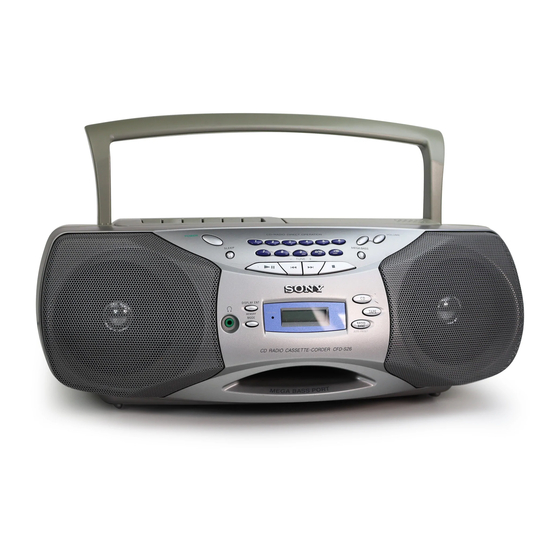
Photo: SILVER
Model Name Using Similar Mechanism CFD-S22/S32
CD
CD Mechanism Type
Section
Optical Pick-up Name
Model Name Using Similar Mechanism CFD-V5
TC
Section Tape Transport Mechanism Type
SPECIFICATIONS
Radio section
Frequency range
FM: 87.6 - 108 MHz
US, E92, MX model:
AM: 530 - 1,710 kHz
SP, AR, AUS, E4 model:
AM: 531 - 1,602 kHz (9 kHz step)
AM: 530 - 1,610 kHz (10 kHz step)
Antennas
FM: Telescopic antenna
AM: Built-in ferrite bar antenna
Cassette-corder section
Recording system
4-track 2 channel stereo
Fast winding time
Approx. 120 sec. with Sony cassette C-60
Frequency response
TYPE I (normal): 80 - 10,000 Hz
CD RADIO CASSETTE-CORDER
US Model
E Model
Australian Model
KSM-213CDP
KSS-213C
MF-V5-117
– Continued on next page –
1
Advertisement
Table of Contents

Related Manuals for Sony CFD-S26


Summary of Contents for Sony CFD-S26
- Page 1 Laser diode properties 4-track 2 channel stereo Material: GaAlAs Fast winding time Wave length: 780 nm Approx. 120 sec. with Sony cassette C-60 Emission duration: Continuous Frequency response Laser output: Less than 44.6 µW TYPE I (normal): 80 - 10,000 Hz...
- Page 2 : Singapore model WITH MARK 0 ON THE SCHEMATIC DIAGRAMS AND IN THE PARTS LIST ARE CRITICAL TO SAFE OPERATION. REPLACE THESE COMPONENTS WITH SONY PARTS WHOSE PART NUMBERS APPEAR AS SHOWN IN THIS MANUAL OR IN SUPPLEMENTS PUBLISHED BY SONY.
-
Page 3: Table Of Contents
CFD-S26 SAFETY CHECK-OUT (US model) TABLE OF CONTENTS After correcting the original service problem, perform the following 1. SERVICING NOTES ............4 safety check before releasing the set to the customer: Check the antenna terminals, metal trim, “metallized” knobs, screws, 2. -
Page 4: Servicing Notes
CFD-S26 SECTION 1 SERVICING NOTES LASER DIODE AND FOCUS SEARCH OPERATION CHUCK PLATE JIG ON REPAIRING CHECK 1. Turn ON the POWER button and press FUNCTION button to On repairing CD section, playing a disc without the lid (CD), use CD position. - Page 5 CFD-S26 – CONTROL (1) BOARD (component side) – CONTROL (1) Board Part No. Former type : 1-679-966-12 New type : 1-679-966-14 – CD BOARD (component side) – – CONTROL (2) BOARD (component side) – CONTROL (2) Board Part No. Former type : 1-679-967-12...
- Page 6 CFD-S26 – BATTERY TERMINAL (1) BOARD (component side) – – BATTERY TERMINAL (2) BOARD (component side) – BATTERY TERMINAL (1) Board Part No. BATTERY TERMINAL (2) Board Part No. Former type : 1-679-964-12 Former type : 1-679-965-12 New type : 1-679-964-14...
-
Page 7: General
CFD-S26 SECTION 2 GENERAL This section is extracted from instruction manual. Location of controls PLAY REW FF STOP/EJECT PAUSE VOLUME +,– Number buttons for CD/RADIO DIRECT OPERATION Tape Z PUSH compartment OPEN/CLOSE SLEEP POWER compartment MEGA BASS TAPE RADIO BAND•... -
Page 8: Disassembly
CFD-S26 SECTION 3 DISASSEMBLY • The equipment can be removed using the following procedure. Cabinet (Upper) Assy Cabinet (Front) Sub Assy Wires Main Board Power (1) Board, Power (2) Board Voltage Select Board Tape Mechanism Block Holder Assy, Cassette PRE Board... -
Page 9: Wires
CFD-S26 3-2. WIRES Put flat cable and wires between the cabinets and push them in the grooves located at A to E in the figure to prevent disconnection before assembling the set. CABINET (FRONT) from MAIN board CABINET (REAR) from speaker from CONTROL (1) board 3-3. -
Page 10: Voltage Select Board
CFD-S26 3-4. VOLTAGE SELECT BOARD (E4 model only) • Abbreviation E4 : AC 110-120V/220-240V area in E model 2 VOLTAGE SELECT board (E4 model only) 1 BVTP 3x10 3-5. CABINET (UPPER) ASSY 4 BVTP 3x12 3 holder assy, cassette 6 BVTP 3x12... -
Page 11: Main Board
CFD-S26 3-6. MAIN BOARD 3 CNP702 6 BVTP 3x10 5 BVTP 3x10 8 MAIN board 2 connector (S801) 1 terminal, antenna 7 CNP301 4 CNP302 3-7. CD MECHANISM BLOCK 1 PWH 2.6x10 2 PWH 2.6x10 3 CD mechanism block (KSM-213CDP) -
Page 12: Tape Mechanism Block
CFD-S26 3-8. TAPE MECHANISM BLOCK 1 BVTP 3x10 2 BVTP 3x10 3 tape mechanism block (MF-V5-117) 3-9. HOLDER ASSY, CASSETTE 1 BVTP 3x10 2 damper 4 holder assy, cassette... -
Page 13: Pre Board
CFD-S26 3-10. PRE BOARD 1 BVTT 2x6 4 PRE board 3 Removal the solders. claw claw 3-11. BELT, M801 (CAPSTAN/REEL MOTOR), HRP301 (HEAD, MAGNETIC) 6 HRP301 (head, magnetic) 1 screws B 2.6x5 mechanism deck 5 claws 4 M801 3 belt... -
Page 14: Optical Pick-Up
CFD-S26 3-12. OPTICAL PICK-UP 2 claws 3 cover, CD 9 optical pick-up 1 claws 5 gear (A) 4 claw 6 claw 8 sled shaft... -
Page 15: Mechanical Adjustments
CFD-S26 SECTION 4 SECTION 5 MECHANICAL ADJUSTMENTS ELECTRICAL ADJUSTMENTS PRECAUTION TAPE SECTION 0 dB = 0.775 V 1. Clean the following parts with a denatured-alcohol-moistened swab : • Standard Output Level record/playback head pinch roller Output terminal HP OUT erase head rubber belts 32 Ω... -
Page 16: Tuner Section
CFD-S26 TUNER SECTION 0 dB = 1 µV FM IF ADJUSTMENT • FM Section Adjust for a maximum reading on level meter. Setting: RADIO (BAND) button: FM 10.7 MHz FM RF signal generator FM FREQUENCY COVERAGE TP (JW2) ADJUSTMENT 0.01 µF Frequency Display 87.5 MHz... -
Page 17: Cd Section
CFD-S26 Adjustment Location: ADJUSTMENT ADJUSTMENT CT1, L1 TP (JW1) FREQUENCY TRACKING – MAIN board (component side) – COVERAGE ADJUSTMENT ADJUSTMENT TP (VT) (CONDUCTOR SIDE) CT3, L3 TRACKING ADJUSTMENT FREQUENCY COVERAGE ADJUSTMENT CD SECTION CD section adjustments are done automatically in this set. -
Page 18: Diagrams
CFD-S26 SECTION 6 DIAGRAMS 6-1. IC PIN DESCRIPTION • IC802 uPD789477-907 (SYSTEM CONTROLLER) Pin No. Pin Name Pin Description 1, 2 — Not used. (Open) 3 – 5 VLC2 – 0 LCD drive voltage output 6 – 9 COM0 – 3 LCD drive common output 10 –... -
Page 19: Circuit Boards Location
CFD-S26 Pin No. Pin Name Pin Description Main system oscillation output (4.19 MHz) System reset input ISS1 ISS1 output Not used. (Open) ISS2 ISS2 output Not used. (Open) EEPROM clock output EEPROM input/output 6-2. CIRCUIT BOARDS LOCATION POWER (1) board... -
Page 20: Block Diagram - Cd Section (Former Type)
CFD-S26 6-3. BLOCK DIAGRAM — CD SECTION (FORMER TYPE) — CD BOARD MAIN BOARD (1/2) CD_IN_ L CNP702(2/2) CNP804(2/2) CNP806(1/3) LCHO INTERPOLATION CNP701 SLICE ERROR MUTE DIGITAL FIN2 EFMIN LEVEL CORRECTION (Page 21) & FILTER CONTROL AUDIO CD RCHO ATTENUATION &... -
Page 21: Block Diagram - Main Section (Former Type)
CFD-S26 6-4. BLOCK DIAGRAM — MAIN SECTION (FORMER TYPE) — PRE BOARD MAIN BOARD (2/2) R.RO R.IN R.LINE CD_IN_R VOLUME/SOUND CONTROLLER REC/PB POWER AMP CNP301 CNP806 IC302 PRE AMP IC304 (Page 20) R-CH (3/3) (3/3) CNP301 (1/3) IC301 L.RO J321... -
Page 22: Printed Wiring Board - Cd Section (Former Type)
CFD-S26 6-5. PRINTED WIRING BOARD — CD SECTION (FORMER TYPE) — • Refer to page 19 for Circuit Boards Location. THIS NOTE IS COMMON FOR PRINTED WIRING BOARDS AND SCHEMATIC DIAGRAMS. (In addition to this, the necessary note is printed in each block.) Common Note on Schematic Diagrams: •... -
Page 23: Schematic Diagram - Cd Section (Former Type)
CFD-S26 6-6. SCHEMATIC DIAGRAM — CD SECTION (FORMER TYPE) — • Refer to page 22 for Common Note on Schematic Diagrams and page 46 for IC Block Diagrams. (Page 26) IC B/D IC B/D • Voltage and waveforms are dc with respect to ground under no-signal (detuned) conditions. -
Page 24: Printed Wiring Boards - Main Section (Former Type)
CFD-S26 6-7. PRINTED WIRING BOARDS — MAIN SECTION (FORMER TYPE) — • Refer to page 19 for Circuit Boards Location and page 22 for Common Note on Printed Wiring Boards. • Semiconductor Location Ref. No. Location ANT1 MAIN BOARD TELESCOPIC... -
Page 25: Schematic Diagram - Main Section (1/4) (Former Type)
CFD-S26 6-8. SCHEMATIC DIAGRAM — MAIN SECTION (1/4) (FORMER TYPE) — • Refer to page 22 for Common Note on Schematic Diagrams and page 46 for IC Block Diagrams. IC B/D IC B/D (Page 26) • Voltage and waveforms are dc with respect to ground under no-signal (detuned) conditions. -
Page 26: Schematic Diagram - Main Section (2/4) (Former Type)
CFD-S26 6-9. SCHEMATIC DIAGRAM — MAIN SECTION (2/4) (FORMER TYPE) — • Refer to page 22 for Common Note on Schematic Diagrams and page 47 for IC Block Diagrams. IC B/D (Page 28) (Page 27) (Page 23) • Waveforms 2V/div 10µsec/div 2V/div 10µsec/div... -
Page 27: Schematic Diagram - Main Section (3/4) (Former Type)
CFD-S26 6-10. SCHEMATIC DIAGRAM — MAIN SECTION (3/4) (FORMER TYPE) — • Refer to page 22 for Common Note on Schematic Diagrams and page 47 for IC Block Diagrams. IC B/D (Page 32) (Page 26) • Voltage is dc with respect to ground under no-signal (detuned) condition. -
Page 28: Schematic Diagram - Main Section (4/4) (Former Type)
CFD-S26 6-11. SCHEMATIC DIAGRAM — MAIN SECTION (4/4) (FORMER TYPE) — • Refer to page 22 for Common Note on Schematic Diagrams and page 47 for IC Block Diagrams. IC B/D (Page 26) • Waveform 0.1V/div 5µsec/div • Voltage and waveforms are dc with respect to ground under no-signal (detuned) conditions. -
Page 29: Printed Wiring Boards - Control Section (Former Type)
CFD-S26 6-12. PRINTED WIRING BOARDS — CONTROL SECTION (FORMER TYPE) — • Refer to page 19 for Circuit Boards Location and page 22 for Common Note on Printed Wiring Boards. (Page 24) MAIN BOARD CNP805 CONTROL ( 1 ) BOARD VOLUME –... -
Page 30: Schematic Diagrams - Control Section (Former Type)
CFD-S26 6-13. SCHEMATIC DIAGRAMS — CONTROL SECTION (FORMER TYPE) — • Refer to page 22 for Common Note on Schematic Diagrams. (Page 26) • Voltage is dc with respect to ground under no-signal (detuned) condition. no mark : FM... -
Page 31: Printed Wiring Boards - Power Supply Section (Former Type)
CFD-S26 6-14. PRINTED WIRING BOARDS — POWER SUPPLY SECTION (FORMER TYPE) — • Refer to page 19 for Circuit Boards Location and page 22 for Common Note on Printed Wiring Boards. BATTERY TERMINAL ( 2 ) BOARD BATTERY TERMINAL ( 1 ) BOARD DRY BATTERY SIZE "... -
Page 32: Schematic Diagrams - Power Supply Section (Former Type)
CFD-S26 6-15. SCHEMATIC DIAGRAMS — POWER SUPPLY SECTION (FORMER TYPE) — • Refer to page 22 for Common Note on Schematic Diagrams. (Page 27) -
Page 33: Block Diagram - Cd Section (New Type)
CFD-S26 6-16. BLOCK DIAGRAM — CD SECTION (NEW TYPE) — CD BOARD MAIN BOARD (1/2) CNP701 CD_IN_ L CNP702 (2/2) CNP804 (2/2) CNP806 (1/3) LCHO INTERPOLATION SLICE ERROR MUTE DIGITAL FIN2 EFMIN LEVEL CORRECTION (Page 34) & FILTER CONTROL AUDIO CD... -
Page 34: Block Diagram - Main Section (New Type)
CFD-S26 6-17. BLOCK DIAGRAM — MAIN SECTION (NEW TYPE) — PRE BOARD MAIN BOARD (2/2) R.RO R.IN R.LINE CD_IN_R VOLUME/SOUND CONTROLLER REC/PB POWER AMP CNP301 CNP806 IC302 PRE AMP IC304 (Page 33) R-CH (3/3) (3/3) CNP301 (1/3) IC301 L.RO J321... -
Page 35: Printed Wiring Board - Cd Section (New Type)
CFD-S26 6-18. PRINTED WIRING BOARD — CD SECTION (NEW TYPE) — • Refer to page 19 for Circuit Boards Location and page 22 for Common Note on Printed Wiring Boards. • Semiconductor Location Ref. No. Location IC701 IC702 Q701 MAIN... -
Page 36: Schematic Diagram - Cd Section (New Type)
CFD-S26 6-19. SCHEMATIC DIAGRAM — CD SECTION (NEW TYPE) — • Refer to page 22 for Common Note on Schematic Diagrams and page 46 for IC Block Diagrams. (Page 39) IC B/D IC B/D • Voltage and waveforms are dc with respect to ground under no-signal (detuned) conditions. -
Page 37: Printed Wiring Boards - Main Section (New Type)
CFD-S26 6-20. PRINTED WIRING BOARDS — MAIN SECTION (NEW TYPE) — • Refer to page 19 for Circuit Boards Location and page 22 for Common Note on Printed Wiring Boards. • Semiconductor Location MAIN BOARD ANT1 Ref. No. Location (Page 35) -
Page 38: Schematic Diagram - Main Section (1/4) (New Type)
CFD-S26 6-21. SCHEMATIC DIAGRAM — MAIN SECTION (1/4) (NEW TYPE) — • Refer to page 22 for Common Note on Schematic Diagrams and page 46 for IC Block Diagrams. IC B/D IC B/D (Page 39) • Voltage and waveforms are dc with respect to ground under no-signal (detuned) conditions. -
Page 39: Schematic Diagram - Main Section (2/4) (New Type)
CFD-S26 6-22. SCHEMATIC DIAGRAM — MAIN SECTION (2/4) (NEW TYPE) — • Refer to page 22 for Common Note on Schematic Diagrams and page 47 for IC Block Diagrams. IC B/D (Page 41) (Page 40) (Page 36) • Waveforms 2V/div 10µsec/div 2V/div 10µsec/div... -
Page 40: Schematic Diagram - Main Section (3/4) (New Type)
CFD-S26 6-23. SCHEMATIC DIAGRAM — MAIN SECTION (3/4) (NEW TYPE) — • Refer to page 22 for Common Note on Schematic Diagrams and page 47 for IC Block Diagrams. IC B/D (Page 45) (Page 39) • Voltage is dc with respect to ground under no-signal (detuned) condition. -
Page 41: Schematic Diagram - Main Section (4/4) (New Type)
CFD-S26 6-24. SCHEMATIC DIAGRAM — MAIN SECTION (4/4) (NEW TYPE) — • Refer to page 22 for Common Note on Schematic Diagrams and page 47 for IC Block Diagrams. IC B/D (Page 39) • Waveform 0.1V/div 5µsec/div • Voltage and waveforms are dc with respect to ground under no-signal (detuned) conditions. -
Page 42: Printed Wiring Boards - Control Section (New Type)
CFD-S26 6-25. PRINTED WIRING BOARDS — CONTROL SECTION (NEW TYPE) — • Refer to page 19 for Circuit Boards Location and page 22 for Common Note on Printed Wiring Boards. (Page 37) MAIN BOARD CNP805 CONTROL ( 1 ) BOARD VOLUME –... -
Page 43: Schematic Diagrams - Control Section (New Type)
CFD-S26 6-26. SCHEMATIC DIAGRAMS — CONTROL SECTION (NEW TYPE) — • Refer to page 22 for Common Note on Schematic Diagrams. (Page 39) • Voltage is dc with respect to ground under no-signal (detuned) condition. no mark : FM... -
Page 44: Printed Wiring Boards - Power Supply Section (New Type)
CFD-S26 6-27. PRINTED WIRING BOARDS — POWER SUPPLY SECTION (NEW TYPE) — • Refer to page 19 for Circuit Boards Location and page 22 for Common Note on Printed Wiring Boards. BATTERY TERMINAL ( 1 ) BOARD BATTERY TERMINAL ( 2 ) BOARD DRY BATTERY SIZE "... -
Page 45: Schematic Diagrams - Power Supply Section (New Type)
CFD-S26 6-28. SCHEMATIC DIAGRAMS — POWER SUPPLY SECTION (NEW TYPE) — • Refer to page 22 for Common Note on Schematic Diagrams. (Page 40) - Page 46 CFD-S26 • IC Block Diagrams IC702 BA6998FP-E2 (CD Board) IC1 TA2149N (MAIN Board) IC701 LC78645E (CD Board) GND1 FM RF FM RF-OUT SP– D.BUFF VCC1 FM RF-IN SL– AM RF-IN D.BUFF AM LOW CUT 78 77 76 75 74 73 72 71...
- Page 47 CFD-S26 IC803 BR24C01AF-WE2 (MAIN Board) IC302 M62429P (MAIN Board) VIN2 VOUT2 CLOCK 1K BIT EEPROM ARRAY VR 2 8BIT 7BIT VOL AMP 2 VREF LOGIC SLAVE • WORD CONTROL ADDRESS DATA ADDRESS 7BIT VOL AMP 1 DECODER REGISTER REGISTER REF AMP...
-
Page 48: Exploded Views
CFD-S26 SECTION 7 EXPLODED VIEWS NOTE: • The mechanical parts with no reference • Color Indication of Appearance Parts The components identified by mark 0 or dotted line with mark number in the exploded views are not supplied. Example : 0 are critical for safety. -
Page 49: Cabinet (Rear) Section
CFD-S26 7-2. CABINET (REAR) SECTION F902 T901 S901 E4 Model US, E92, MX, AUS, SP, AR Model The components identified by mark 0 or dotted line with mark 0 are critical for safety. Replace only with part number specified. Ref. No. -
Page 50: Cabinet (Upper) Section
CFD-S26 7-3. CABINET (UPPER) SECTION ANT1 S801 MF-V5-117 KSM-213CDP LCD801... - Page 51 CFD-S26 Ref. No. Part No. Description Remark Ref. No. Part No. Description Remark * 101 A-3062-378-A MAIN BOARD, COMPLETE (SP) 3-922-112-21 DAMPER * 101 A-3062-379-A MAIN BOARD, COMPLETE (E4) 3-224-369-01 CABINET (UPPER) (SILVER) * 101 A-3062-386-A MAIN BOARD, COMPLETE (AR)
-
Page 52: Tape Mechanism Section-1
CFD-S26 7-4. TAPE MECHANISM SECTION-1 (MF-V5-117) HRP301 HE301 Ref. No. Part No. Description Remark Ref. No. Part No. Description Remark 3-933-010-01 SPRING (S/P), TORSION * 162 3-008-587-01 SLIDER (STOP) 3-933-025-01 SPRING (P), TORSION * 163 3-008-591-01 SLIDER (PAUSE) 3-040-857-01 LEVER (P) -
Page 53: Tape Mechanism Section-2
CFD-S26 7-5. TAPE MECHANISM SECTION-2 (MF-V5-117) S802 M801 Ref. No. Part No. Description Remark Ref. No. Part No. Description Remark 3-933-029-01 LEVER, ERASING PREVENTION X-3377-877-2 FLYWHEEL ASSY 3-933-182-01 SPRING, CASSETTE 3-932-993-01 CHASSIS, OUTSERT 3-932-995-01 GEAR (MID) 3-343-358-01 RING, RETAINING X-3371-667-1 CLUTCH ASSY... -
Page 54: Optical Pick-Up Section
CFD-S26 Ver 1.2 7-6. OPTICAL PICK-UP SECTION (KSM-213CDP) not supplied M701 M702 The components identified by mark 0 or dotted line with mark 0 are critical for safety. Replace only with part number specified. Ref. No. Part No. Description Remark Ref. -
Page 55: Electrical Parts List
CFD-S26 SECTION 8 BATTERY TERMINAL (1) ELECTRICAL PARTS LIST BATTERY TERMINAL (2) NOTE: The components identified by • Due to standardization, replacements in • Items marked “*” are not stocked since mark 0 or dotted line with mark the parts list may be different from the they are seldom required for routine service. - Page 56 CFD-S26 Ref. No. Part No. Description Remark Ref. No. Part No. Description Remark JC704 1-216-813-11 METAL CHIP 1/16W A-3347-089-A CD BOARD, COMPLETE (NEW) ******************* < FERRITE BEAD > < CAPACITOR > L706 1-414-445-11 FERRITE, EMI (SMD) C701 1-162-964-11 CERAMIC CHIP 0.001uF...
- Page 57 CFD-S26 CONTROL (1) Ref. No. Part No. Description Remark Ref. No. Part No. Description Remark < FERRITE BEAD > R743 1-216-831-11 METAL CHIP 6.8K 1/16W R744 1-216-845-11 METAL CHIP 100K 1/16W FB701 1-469-701-21 INDUCTOR, FERRITE BEAD < SWITCH > < IC >...
- Page 58 CFD-S26 CONTROL (1) CONTROL (2) Ref. No. Part No. Description Remark Ref. No. Part No. Description Remark R442 1-216-815-11 METAL CHIP 1/16W R421 1-216-823-11 METAL CHIP 1.5K 1/16W R422 1-216-827-11 METAL CHIP 3.3K 1/16W < SWITCH > R423 1-216-831-11 METAL CHIP 6.8K...
- Page 59 CFD-S26 CONTROL (2) CONTROL (3) MAIN Ref. No. Part No. Description Remark Ref. No. Part No. Description Remark < SWITCH > 1-679-968-11 CONTROL (3) BOARD (NEW) ****************** S407 1-786-050-21 SWITCH, KEYBOARD (CD) S408 1-786-050-21 SWITCH, KEYBOARD (TAPE) < DIODE >...
- Page 60 CFD-S26 MAIN Ref. No. Part No. Description Remark Ref. No. Part No. Description Remark 1-162-960-11 CERAMIC CHIP 220PF C224 1-164-227-11 CERAMIC CHIP 0.022uF 25V (SP) 1-162-927-11 CERAMIC CHIP 100PF C225 1-162-966-11 CERAMIC CHIP 0.0022uF 10% 1-162-927-11 CERAMIC CHIP 100PF C226 1-126-959-11 ELECT 0.47uF...
- Page 61 CFD-S26 MAIN Ref. No. Part No. Description Remark Ref. No. Part No. Description Remark C953 1-126-935-11 ELECT 470uF < JUMPER RESISTOR > C957 1-162-974-11 CERAMIC CHIP 0.01uF C959 1-104-665-11 ELECT 100uF 1-216-864-11 METAL CHIP 1/16W C960 1-162-974-11 CERAMIC CHIP 0.01uF...
- Page 62 CFD-S26 MAIN Ref. No. Part No. Description Remark Ref. No. Part No. Description Remark Q818 8-729-054-21 TRANSISTOR KRC407-RTK R144 1-216-789-11 METAL CHIP 1/16W Q819 8-729-054-18 TRANSISTOR KRC404-RTK R145 1-216-827-11 METAL CHIP 3.3K 1/16W Q820 8-729-054-23 TRANSISTOR KRC409-RTK R225 1-216-827-11 METAL CHIP 3.3K...
- Page 63 CFD-S26 MAIN Ref. No. Part No. Description Remark Ref. No. Part No. Description Remark R835 1-216-841-11 METAL CHIP 1/16W A-3062-378-A MAIN BOARD, COMPLETE (SP) (NEW) R836 1-216-841-11 METAL CHIP 1/16W A-3062-379-A MAIN BOARD, COMPLETE (E4) (NEW) R837 1-216-809-11 METAL CHIP...
- Page 64 CFD-S26 MAIN Ref. No. Part No. Description Remark Ref. No. Part No. Description Remark 1-162-915-11 CERAMIC CHIP 10PF 0.5PF C271 1-126-964-11 ELECT 10uF 1-136-169-00 FILM 0.22uF C303 1-126-933-11 ELECT 100uF 16V (US) 1-126-176-11 ELECT 220uF C321 1-126-935-11 ELECT 470uF 1-162-927-11 CERAMIC CHIP...
- Page 65 CFD-S26 MAIN Ref. No. Part No. Description Remark Ref. No. Part No. Description Remark < CONNECTOR > 1-216-864-11 METAL CHIP 1/16W JC11 1-216-864-11 METAL CHIP 1/16W * CNP302 1-815-552-11 PIN, CONNECTOR (PC BOARD) 4P JC12 1-216-864-11 METAL CHIP 1/16W * CNP323 1-815-445-11 PIN, CONNECTOR 4P...
- Page 66 CFD-S26 MAIN Ref. No. Part No. Description Remark Ref. No. Part No. Description Remark Q955 8-729-021-82 TRANSISTOR 2SD2396K R142 1-216-827-11 METAL CHIP 3.3K 1/16W Q957 8-729-212-02 TRANSISTOR 2SC2120-Y R143 1-216-853-11 METAL CHIP 470K 1/16W R144 1-216-789-11 METAL CHIP 1/16W < RESISTOR >...
- Page 67 CFD-S26 MAIN POWER (1) Ref. No. Part No. Description Remark Ref. No. Part No. Description Remark R820 1-216-864-11 METAL CHIP 1/16W < TRANSFORMER > (E92,MX) R821 1-216-829-11 METAL CHIP 4.7K 1/16W 1-433-741-11 TRANSFORMER, IF (US,E4,AUS,SP,AR) 1-419-465-11 COIL (DET) R822 1-216-835-11 METAL CHIP...
- Page 68 CFD-S26 POWER (1) POWER (2) Ref. No. Part No. Description Remark Ref. No. Part No. Description Remark C906 1-126-964-11 ELECT 10uF C204 1-162-966-11 CERAMIC CHIP 0.0022uF 10% C205 1-162-923-11 CERAMIC CHIP 47PF < AC INLET > C206 1-126-960-11 ELECT C207...
- Page 69 CFD-S26 VOLTAGE SELECT Ref. No. Part No. Description Remark Ref. No. Part No. Description Remark R308 1-216-837-11 METAL CHIP 1/16W ACCESSORIES & PACKING MATERIALS R309 1-216-805-11 METAL CHIP 1/16W ******************************* < SWITCH > 1-557-287-11 CORD, POWER (E92,MX) 1-569-008-21 ADAPTOR, CONVERSION (E4)
- Page 70 CFD-S26 MEMO...
- Page 71 CFD-S26 US Model E Model SERVICE MANUAL SERVICE MANUAL Australian Model Ver 1.2 2002. 06 SUPPLEMENT-1 File this supplement with the service manual. Subject : Change of CD Mechanism (SPM-02027) CD mechanism changed to KSM-213RDP from KSM-213CDP after serial No. 2341962.
- Page 72 CFD-S26 CD MECHANISM SECTION (KSM-213RDP) M701 The components identified by M702 mark 0 or dotted line with mark 0 are critical for safety. Replace only with part number specified. Ref. No. Part No. Description Remark Ref. No. Part No. Description...
- Page 73 CFD-S26 MEMO...
- Page 74 CFD-S26 REVISION HISTORY Clicking the version allows you to jump to the revised page. Also, clicking the version at the upper on the revised page allows you to jump to the next revised page. Ver. Date Description of Revision 2001. 03 2001.