Sony DVP-NC625 Service Manual
Cd/dvd player
Hide thumbs
Also See for DVP-NC625:
- Operating instructions manual (77 pages) ,
- Manual (51 pages) ,
- Limited warranty (1 page)
Table of Contents
Advertisement
Quick Links
DVP-NC625/NC665P
SERVICE MANUAL
System
Laser: Semiconductor laser
Signal format system:
NC625: US,CND,PX,E,MX: NTSC
NC665P: US,CND: NTSC
NC625: SP,AUS: PAL/NTSC
NC625: AEP,UK: PAL/(NTSC)
Audio characteristics
Frequency response: DVD VIDEO (PCM
96kHZ): 2Hz to 44 kHZ (±1.0 dB)/
DVD VIDEO (PCM 48 kHZ): 2Hz tO
22 kHz (±0.5 dB)/CD: 2Hz to 20 kHz
(±0.5 dB)
Singal-to nosie ratio (S/N ratio): 115 dB
(LINE OUT L/R (AUDIO) jacks only)
Harmonic distortion: 0.003%
Dynamic range: DVD VIDEO: 103 dB/
CD:99 dB
Wow and flutter: Less than detected value
(±0.001% W PEAK)
The signals from LINE OUT L/R
(AUDIO) jacks are measured. When you
play PCM sound tracks with a 96 kHz
sampling frequency, the output signals
from the DIGITAL OUT (COAXIAL) jack
are converted to 48 kHz sampling
frequency.
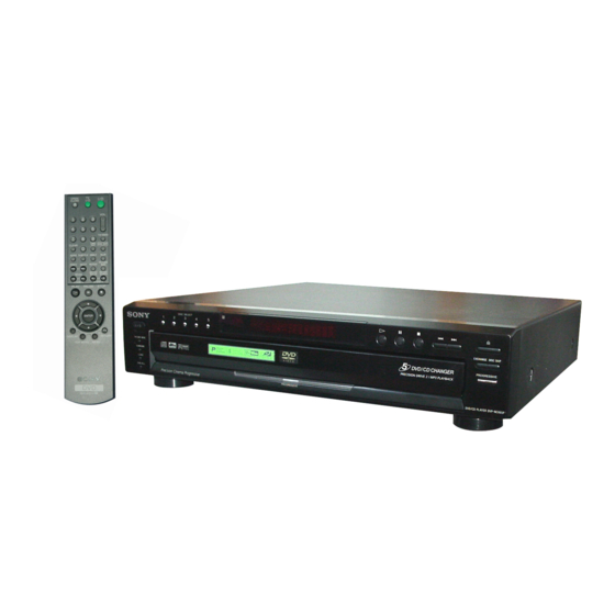
Photo : DVP-NC665P (BLACK)
RMT-D155P
SPECIFICATIONS
Outputs
(Jack name: Jack type/Output level/Load
impedance)
LINE OUT L/R (AUDIO): Phono jack/
2 Vrms/10 kilohms
DIGITAL OUT (COAXIAL): Phono
jacks/0.5 Vp-p/75 ohms
DIGITAL OUT (OPTICAL): Optical
output jack/–18 dBm (wave length:
660nm)
(NC625:SP,AUS/NC665P:CND)
COMPONENT VIDEO OUT (Y,P
C
/C
): Phono jack/Y: 1.0Vp-p/
B
R
PB,PR,CB,CR:0.7Vp-p/75 ohms.
Y: 1.0 ± 0.1 Vp-p
Cb: 646 ± 50mVp-p
Cr: 646 ± 50mVp-p (NC625:US,CND/
NC665P:US,CND)
R,G,B: 700 ± 50Vp-p
(NC625:UK,AEP)
LINE OUT (VIDEO): Phono jack/
1.0 Vp-p/75 ohms
S VIDEO OUT: 4-pin mini DIN/
Y: 1.0Vp-p/C:0.3 Vp-p (PAL),
0.286 Vp-p (NTSC)/75 ohms
(NC625:SP,AUS,US,CND,PX,MX,E/
NC665P)
RMT-D154A/D155A/D155P
Canadian Model
Mexico Model
Singapore Model
Australia Model
General
Power requirements:
120V AC, 60Hz
(NC665P/NC625:US,CND,MX,E)
110 to 240V AC, 50/60 Hz
(NC625:UK,SP,AUS,CND,MX,E,US,PX)
See Page 1-1 for further information.
Power consumption:
14W (DVP-NC625:
US,CND,PX,E,MX,SP,AUS)/
15W (DVP-NC665P: US/
/P
,
NC625: AEP,UK)
B
R
See page 1-1 for further information.
Dimensions (approx):
430 × 95.5 × 409mm
(17 × 3
× 16
/
6
8
depth) incl. projecting parts
Mass (approx): 5.1kg (11 1b 4 oz)
Operating temperature: 5°C to 35°C
(41°F to 95°F)
Operating humidity: 25% to 80%
Supplied accessories
See Page 14. (NC625:CND,US,PX)
See Page 15. (NC625:AEP,MX,E,
UK,SP,AUS/NC665P)
See Page 16. (NC625:AEP)
Specifications and design are subject to
change without notice.
®
E
is a U.S. registered mark.
NERGY STAR
As an E
NERGY STAR
Corporation has determined that this
product meets the E
for energy efficiency.
(NC625:CND,US,CND,US,PX/NC665P)
CD/DVD PLAYER
US Model
DVP-NC625/NC665P
PX Model
E Model
AEP Model
UK Model
DVP-NC625
/
in.) (width/height/
1
18
®
Partner, Sony
®
guidelines
NERGY STAR
Advertisement
Table of Contents

Related Manuals for Sony DVP-NC625


Summary of Contents for Sony DVP-NC625
- Page 1 Vp-p/75 ohms See Page 1-1 for further information. DIGITAL OUT (OPTICAL): Optical Power consumption: Audio characteristics output jack/–18 dBm (wave length: 14W (DVP-NC625: 660nm) US,CND,PX,E,MX,SP,AUS)/ Frequency response: DVD VIDEO (PCM (NC625:SP,AUS/NC665P:CND) 15W (DVP-NC665P: US/ 96kHZ): 2Hz to 44 kHZ (±1.0 dB)/...
- Page 2 ON THE SCHEMATIC DIAGRAMS AND IN THE PARTS CRITIQUES POUR LA SÉCURITÉ DE FONCTIONNEMENT. NE LIST ARE CRITICAL TO SAFE OPERATION. REPLACE THESE REMPLACER CES COMPOSANTS QUE PAR DES PIÈSES SONY COMPONENTS WITH SONY PARTS WHOSE PART NUMBERS DONT LES NUMÉROS SONT DONNÉS DANS CE MANUEL OU APPEAR AS SHOWN IN THIS MANUAL OR IN SUPPLEMENTS DANS LES SUPPÉMENTS PUBLIÉS PAR SONY.
-
Page 3: Table Of Contents
DVP-NC625/NC665P TABLE OF CONTENTS SERVICE NOTE Note on Removing the Upper Case ......5 Custom Settings (CUSTOM SETUP) ......1-15 Disc Removal Procedure .......... 5 Settings for the Sound (AUDIO SETUP) ....1-16 Note on Removing the Table Ass’y ......5 Additional Information ........... - Page 4 DVP-NC625/NC665P • ER-14 (Line1 Out) TEST MODE Printed Wiring Board ........4-33 6-1. General Description ..........6-1 • ER-14 Board (AEP,UK Model only) 6-2. Starting Test Mode ..........6-1 Line1 Out Schematic Diagram ....... 4-35 6-3. Syscon Diagnosis ..........6-1 •...
-
Page 5: Service Note
DVP-NC625/NC665P SERVICE NOTE NOTE ON REMOVING THE UPPER NOTE ON REMOVING THE TABLE CASE ASS’Y Remove the four tapping screws and three screws. (See Fig. 1) Remove the two screws. (See Fig. 3) Open the sides of case. (See Fig. 1) Remove the upper case in the direction of the arrow A. -
Page 6: Note On Mounting The Gears
DVP-NC625/NC665P NOTE ON MOUNTING THE GEARS Mount the gear (chuck). (See Fig. 5) Mount the gear (idler) while aligning the engagement of the Rotate the gear (chuck) in the direction of the arrow. (down gear (swing) and the gear (chuck). (See Fig. 7) position) (See Fig. - Page 7 DVP-NC625/NC665P HOW TO SERVICE THE MB-108 Remove the upper case from the set. (Refer to section 2-1) Remove the MB-108 board. (Refer to section 2-4) BOARD Set the MB-108 board in the stand (with CK-121 board) as shown in Fig. 9.
- Page 8 DVP-NC625/NC665P Set the four flexible flat cables as shown in Fig. 11. Flexible flat cable (FFC 9P: CN204) Connector (CN102) Flexible flat cable (FFC 26P: CN203) MB-108 Connector (CN104) Connector (CN301) Fig. 11. Set the flexible flat cable and the harness as shown in Fig. 12.
-
Page 9: Connection Of Service Jig
DVP-NC625/NC665P CONNECTION OF SERVICE JIG AV-072 board CN201 FFC25P CK-120 board CN601 FFC 26P (Used the set) FFC 26P CN101 CN102 CN203 FFC 9P (Used the set) FFC 9P CN103 CN104 CN204 Mechanism deck MB-108 board FFC 11P CN107 CN108... - Page 10 DVP-NC625/NC665P MEMO — 10E — — 10 —...
-
Page 11: General
• If the player is brought directly from a cold concerning your player, please consult your to a warm location, or is placed in a very nearest Sony dealer. damp room, moisture may condense on the lenses inside the player. Should this occur, the player may not operate properly. - Page 12 Disc numbers (28) Playing time of the Lights up when you can change the angle (53) current title (46) Disc type Current disc All discs Playing Lights up during Repeat Play (39) mode (36) status A DIGITAL OUT (COAXIAL) jack (21) D LINE OUT (VIDEO) jack (16) Current audio signal (49) E S VIDEO OUT jack (16)
-
Page 13: Hookups
ALL DISCS/ONE DISC (page 36) Selects All Discs or One Disc mode. Item Item Name, Function, Relevant Disc Type DISC (page 42) PROGRAM (page 36) Selects the disc to be played. Selects the disc, title, chapter, or track to play in the order you want. TITLE (page 42)/SCENE (page 42)/TRACK (page 42) Selects the title, scene, or track to be played. - Page 14 Film based software, regardless of the type of software that you are playing. is recommended that you switches the connection to the standard definition output. If there are questions regarding your Sony TV set’s compatibility with this model 480p DVD player, please contact our customer service center.
- Page 15 If the stereo amplifier (receiver) has audio input jacks L and R only, use . If the amplifier You can enjoy the Dolby Surround effects only when playing Dolby Surround audio or multi- (receiver) has a digital input jack, or when connecting to an MD deck or DAT deck, use channel audio (Dolby Digital) discs.
-
Page 16: Playing Discs
AUDIO SETUP AUDIO ATT: AUDIO DRC: STANDARD DOWNMIX: DOLBY SURROUND DIGITAL OUT: To enjoy the surround sound effects of this DOLBY DIGITAL: D-PCM • 4:3 LETTER BOX or 4:3 PAN SCAN DTS: D-PCM player or your amplifier (receiver), set the (page 65) DOLBY DIGITAL following items as described below for the... - Page 17 Repeat Play mode (page 39), the current disc Notes starts playing again. – In All Discs Shuffle Play mode (page 38), titles/ • The point where you stopped playing is cleared tracks/chapters are reshuffled only on the current when: disc. You can open the disc tray while playing a –...
- Page 18 z Hint To play without using PBC, press ./> while the player is stopped to select a track, then press H You can play MP3 audio tracks on CD-ROMs or ENTER. or CD-Rs/CD-RWs. However, the discs must “Play without PBC.” appears on the TV screen and The list of MP3 albums recorded on the be recorded according to ISO9660 level 1, the player starts continuous play.
-
Page 19: The Disc (Resume Play/Multi-Disc Resume)
1 2 ( 2 7 ) STOP Program Play begins. 1 8 ( 3 4 ) DVD VIDEO When the program ends, you can restart the same program again by pressing H. For example, select chapter “03” of title You can have the player “shuffle” titles, “02.”... -
Page 20: Searching For A Scene
Playback direction ×2B t FF1M t FF2M t FF3M Searching for a Scene When the player is in the pause mode, press FF3M (DVD VIDEO/DVD-RW/ to go to the next frame. Press VIDEO CD only) ×2B (DVD VIDEO/CD only) to go to the preceding frame (DVD only). -
Page 21: Viewing Information About The Disc
Viewing Information About the • T * : * : * Disc Track playing time and current disc Playing time of the current title track number You can view the time information and text • T– * : * : * displayed on the TV screen also on the front Remaining time of the current title panel display. -
Page 22: Sound Adjustments
(L: left, R: right) without using actual rear speakers. TVS was developed by Sony to produce Select “OFF” in step 2. surround sound for home use using just a stereo TV. - Page 23 The disc plays with the setting you Enjoying Movies selected. If subtitles are recorded on the discs, you can change the subtitles or turn them on and off Select “OFF” in step 3. The Block Noise Reduction (BNR) function whenever you want while playing a DVD. adjusts the picture quality by reducing the If various angles (multi-angles) for a scene “block noise”...
-
Page 24: Using Various Additional Functions
Using Various Additional The disc plays with the setting you Functions selected. The options for “PARENTAL CONTROL” appear. STOP 1 2 ( 2 7 ) DVD VIDEO 1 8 ( 3 4 ) Select “OFF” in step 3. 1 : 3 2 : 5 5 You can set two kinds of playback restrictions Press DISPLAY repeatedly until the Control PLAYER... -
Page 25: Settings And Adjustments
The Control Menu appears. You can control the sound level, input source, and power switch of non-Sony TVs as well. If you to enter a new 4-digit password. After you enter and power switch of your Sony TV with the... - Page 26 Note Selects the black level (setup level) for the Depending on the DVD, “4:3 LETTER BOX” may video signals output from the COMPONENT be selected automatically instead of “4:3 PAN VIDEO OUT jacks. SCAN” or vice versa. You cannot select this when the player outputs progressive signal and the Choose settings according to the TV to be Use this to set up playback related and other...
-
Page 27: Additional Information
Should any problem persist, consult your is not correctly finalized (page 6). motion Play mode. nearest Sony dealer (for customers in the , The player is in fast forward or fast reverse , Depending on the disc, you may not be able U.S.A only). - Page 28 The longest section of a picture or music feature on a DVD, movie, etc., in video DVDs can be classified as Film based or software, or the entire album in audio Video based software. Film based DVDs For details, see pages 49, 53, 64. software.
-
Page 29: Disassembly
DVP-NC625/NC665P SECTION 2 DISASSEMBLY 2-1. DISASSEMBLY • This set can be disassembled in the order shown below. Upper case (Page 2-1) Front panel section Rear panel section MB-108 board DV-034 board Power block (Page 2-2) (Page 2-2) (Page 2-3) (Page 2-3) (Page 2-6) Table ass’y... -
Page 30: Front Panel Section
2-3. FRONT PANEL SECTION Connector (CN2) Harness AV-072 Board PF-134 Two screws (B3) Connector (CN403) Connector (CN471) Connector (CN202) Flexible flat cable (FFC-FDS-003: CN308) Connector Claw Two scre (CN306) Harness (B3) FV-121 Connector (CN402) Cover Tray Front panel section 2-4. REAR PANEL Screw (B3) Rear panel Connector... -
Page 31: Board
2-5. MB-108 BOARD Flexible flat cable (FMM-42(26P): CN203) Four screws (B3) Flexible flat cable (FMO-6(9P): CN204) Connector MB-108 board (CN102) Pull the tray in the direction of the arrow Flexible flat cable (FMV-20(25P): CN601) Board to board connector (CN101) Flexible flat cable (FMC-15(11P): CN201) Insert a flat-head (-) screwdriver into a hole at the bottom, and rotate the cam gear in the direction of the arrow... -
Page 32: Er-14 Board (Aep, Uk)
2-7. AV-072 BOARD Six screws (B3)(NC665P) Flexible flat cable Five screws (FAE-10: CN102 ) (B3)(NC625) (EC1,EC2,CEK) Screw Qty USA/Canada ECI & CEK MX2 & E32 AV-072 board 2-8. ER-14 BOARD (AEP, UK) Two screws (B3) Flexible flat cable (FAE-10: CN901) ER-14 board 2-9. -
Page 33: Loading Motor Ass'y
2-10. LOADING MOTOR ASS’Y Belt (timing) ✕ Screw (M2.6 MD-94 board ✕ Screw (M2.6 ✕ Screw (M2.6 Loading motor assembly (M901) Connector (CN004) Claw Claws 2-11. OPTICAL PICK-UP Two screws (B3) Chuck assy Three step screws Optical pick-up Flexible flat cable (FMM-42, 26P) Flexible flat cable (FMO-6, 9P) - Page 34 2-12.POWER BLOCK Two claws Power block Connector Holder, PS (CN1) Harness (CN2) Two screws (B3) 2-13.IF-099 AND FR-197 BOARDS NC625 Screw (B2.6 x 8), +BVTP 4-951-620-01 NC665P Harness (FP-176(3p) CN701) Flexib le flat cab (FDS-003) Front panel...
- Page 35 2-14.INTERNAL VIEWS PH101 (on the SE-130 board) PH102 Optical pick-up (on the SE-130 board) (KHM-290AA/Ser vice assembly) A-6061-908-A TD unit ass'y A-6060-640-A Encoder ass'y (loading) X-3952-380-1 M901 Loading motor ass'y X-3952-378-1...
-
Page 36: Power Block
2-15.CIRCUIT BOARDS LOCATION POWER BLOCK (SWITCHING REGULATOR) SE-130 board (SENSOR) ER-14 board MD-94 board (LINE1 OUT) (MD INTERFACE) AV-072 board (AUDIO/VIDEO OUT) FR-197 board MB-108 board (FUNCTION SW) DVD/CD RF AMP, DIGITAL SERVO, PL-032 board MOTOR DRIVE, AV DECODER, *NC665P only SDRAM, SYSTEM CONTROL, (LED) AUDIO DAC, PLL, I/P CONVERTER,... -
Page 37: Block Diagrams
DVP-NC625/NC665P SECTION 3 BLOCK DIAGRAMS 3-1. OVERALL BLOCK DIAGRAM MB-108 BOARD AV-072 BOARD (SEE PAGE 4-9 to 4-20) (SEE PAGE 4-27) NC665P only IC404, 405 IC503 16M SDRAM J102 SDRAM Y, Cb, Cr COMPONENT VIDEO OUT IC303 V, Y, C... -
Page 38: System Control Block Diagram
DVP-NC625/NC665P 3-2. SYSTEM CONTROL BLOCK DIAGRAM MB-108 BOARD (1/6) (SEE PAGE 4-9) IC108 IC106 IC107 1M SRAM 32M FLASH HA 0 – 21 HA 0 – 21 HD 0 – 15 HD 0 – 15 IC104 tf 1 – 5 102 – 109 111 – 118 120 85 – 100 59 72 84 HA 0 –... -
Page 39: Rf/Servo Block Diagram
DVP-NC625/NC665P 3-3. RF/SERVO BLOCK DIAGRAM IC201 tl IC201 2 (CD PB) IC201 2 (DVD PLAY) IC201 rs (CD PB) IC201 rs (DVD PLAY) 890nsec 1.3Vp-p 20nsec 0.47Vp-p 20nsec 0.79Vp-p 433mVp-p 383mVp-p BASE UNIT KHM-290AAA/SERVICE ASSY MB-108 BOARD (2/6) IC301 (CD PB) -
Page 40: Signal Processor Block Diagram
DVP-NC625/NC665P 3-4. SIGNAL PROCESSOR BLOCK DIAGRAM MB-108 BOARD (3/6) *IC405: AEP, UK, RUS, (SEE PAGE 4-13) HK, SP, TW, KR, ME2, IC404, 405* ME5, EA, AUS 16M SDRAM IC301 <zzz (DVD PLAY) IC303 16M DRAM 40ns/div 1.34Vp-p 301 <zzc (CD PB) NC625 ONLY 105 –... -
Page 41: Audio Block Diagram
DVP-NC625/NC665P 3-5. AUDIO BLOCK DIAGRAM AV-072 BOARD (2/2) MB-108 BOARD (6/6) (SEE PAGE 4-29) (SEE PAGE 4-19) SP,AUS,US,CANADIAN IC204 1 D IN OPTICAL DIGITAL CN601 (3/3) CN203 (2/2) J201 SPDIF Q211 COAXIAL SPDIF BUFFER IC601 1 IC601 SIGNAL PROCESSOR IC201... -
Page 42: Video Block Diagram (Nc625)
DVP-NC625/NC665P 3-6. VIDEO BLOCK DIAGRAM (NC625) AV-072 BOARD (1/2) * IC102 36 pin : EXCEPT AEP, UK J101 (1/2) IC102 ed (SEE PAGE 4-27) 24 pin : AEP, UK EXCEPT AEP, UK IC102 VIDEO BUFFER CN201 (1/2) LINE OUT AEP, UK... -
Page 43: Video Block Diagram (Nc665P)
DVP-NC625/NC665P 3-7. VIDEO BLOCK DIAGRAM (NC665P) MB-108 BOARD AV-72 BOARD J104 (SEE PAGE 4-17) (SEE PAGE 4-27) VIDEO LINE OUT MCLOCK DVD 0 – 7 PI 2 - 9 SIGNAL AO 0 – 11 IC503 PROCESSER MA 0 - 11... -
Page 44: Interface Control Block Diagram
DVP-NC625/NC665P 3-8. INTERFACE CONTROL BLOCK DIAGRAM IF-099 BOARD (SEE PAGE 4-39) IC404 IC406 IF CON REMOTE COMMANDER RECEIVER CN407 AUDIO A MUTE (SEE PAGE 3-9) /AMUTE VIDEO VMUTE /VMUTE (SEE PAGE 3-11 to 3-14) FR-197 BOARD SW-385 BOARD (SEE PAGE 4-49) -
Page 45: Power Block Diagram (1/3)
DVP-NC625/NC665P 3-9. POWER BLOCK DIAGRAM (1/3) SWITCHING REGULATOR (DPS-21BPA) : (NC625: US, CND, MX/ NC665P: US, CND) L301 D301 SW+11V T101 Q401 L205 D201 L201 EVER+11V • F101 Q101 D101 L101 SW+5V D1A-1D AC IN FL1, 2 LINE FILTER F301... -
Page 46: Power Block Diagram (2/3)
DVP-NC625/NC665P 3-10.POWER BLOCK DIAGRAM (2/3) SWITCHING REGULATOR (ETXNY410M0F): (NC625: E, AEP, UK, SP, AUS) CN201 Q301 L301 D301 SW+11V • T101 L205 D201 L201 EVER+11V Q203 D202 F201 L202 SW+5V D104-D CN101 AC IN F101 L101, 102 LINE FILTER Q204... -
Page 47: Power Block Diagram (3/3)
DVP-NC625/NC665P 3-11.POWER BLOCK DIAGRAM (3/3) DVP-NC625 AEP, UK IF-099 BOARD AV-072 BOARD ER-14 BOARD (SEE PAGE 4-39) (SEE PAGE 4-29) (SEE PAGE 4-35) CN102 CN801 +11V IC901 +11V CN471 PS472 CN402 CN202 VIDEO EVER +11V BUFFER SELECT SWITCH IC101 PS471 Q472, 473 EVER -15.5V... -
Page 48: Printed Wiring Boards And Schematic Diagrams
DVP-NC625/NC665P SECTION 4 PRINTED WIRING BOARDS AND SCHEMATIC DIAGRAMS 4-1. FRAME SCHEMATIC DIAGRAM FRAME SCHEMATIC DIAGRAM... -
Page 49: Printed Wiring Boards And Schematic Diagram
DVP-NC625/NC665P 4-2. PRINTED WIRING BOARDS AND SCHEMATIC DIAGRAMS THIS NOTE IS COMMON FOR WIRING BOARDS AND SCHEMATIC DIAGRAMS (In addition to this, the necessary note is printed in each block) (For printed wiring boards) (For schematic diagrams) • All capacitors are in µF unless otherwise noted. pF : µµF. -
Page 50: Waveforms
DVP-NC625/NC665P MB-108 BOARD AV-072 BOARD IF-099 BOARD ER-14 BOARD IC901 wg IC103 3 IC201 ra (DVD PLAY) IC301 (CD PB) IC403 yd IC504 el IC102 ed IC404 2 3.4Vp-p 2.4Vp-p (H) 1.7Vp-p 8 MHz 770mVp-p 3.3Vp-p 625mVp-p 131Vp-p 2.0Vp-p 21msec 6.8usec... - Page 51 DVP-NC625/NC665P MB-108 (DVD/CD RF AMP,DIGITAL SERVO,MOTOR DRIVE,SERVO,AV DECODER,SD RAM, • : Uses unleaded solder. SYSTEM CONTROL,AUDIO DAC,PLL) PRINTED WIRING BOARD MB-108 BOARD (SIDE A) MB-108 BOARD SIDE B MB-108 BOARD For printed wiring board POWER BLOCK A SIDE B SIDE...
-
Page 52: System Control
DVP-NC625/NC665P For Schematic Diagram • Refer to page 4-7 for printed wiring board of MB-108 board. • Refer to page 4-5 for waveform MB-108 BOARD (1/6) SYSTEM CONTROL -REF.NO.:1000 SERIES- XX MARK:NO MOUNT NO MARK:REC/PB MODE The components identified by Les composants identifiés par... -
Page 53: Schematic Diagram
DVP-NC625/NC665P For Schematic Diagram • Refer to page 4-7 for printed wiring board of MB-108 board. • Refer to page 4-5 for waveform MB-108 BOARD (2/6) MOTOR DRIVE -REF.NO.:2000 SERIES- XX MARK:NO MOUNT NO MARK:PB MODE -0.05 -0.05 0.04 0.03 0.03... - Page 54 DVP-NC625/NC665P For Schematic Diagram • Refer to page 4-7 for printed wiring board of MB-108 board. • Refer to page 4-5 for waveform MB-108 BOARD (3/6) SERVO -REF.NO.:3000 SERIES- XX MARK:NO MOUNT NO MARK:PB MODE 1.3 3.3 -0.03 -0.04 SIGNAL PATH...
-
Page 55: Schematic Diagram
DVP-NC625/NC665P For Schematic Diagram • Refer to page 4-7 for printed wiring board of MB-108 board. • Refer to page 4-5 for waveform MB-108 BOARD (4/6) AV DECODER -REF.NO.:4000 SERIES- XX MARK:NO MOUNT NO MARK:PB MODE 0.12 0.03 -0.05 0.04... - Page 56 DVP-NC625/NC665P For Schematic Diagram • Refer to page 4-7 for printed wiring board of MB-108 board. • Refer to page 4-5 for waveform MB-108 BOARD (5/6) 1/P CONVERTER -REF.NO.:5000 SERIES- XX MARK:NO MOUNT NO MARK:PB MODE SIGNAL PATH VIDEO SIGNAL...
-
Page 57: Schematic Diagram
DVP-NC625/NC665P For Schematic Diagram • Refer to page 4-7 for printed wiring board of MB-108 board. • Refer to page 4-5 for waveform MB-108 BOARD (6/6) AUDIO DAC, PLL -REF.NO.:6000 SERIES- XX MARK:NO MOUNT NO MARK:PB MODE TO AV-072 BOARD... - Page 58 DVP-NC625/NC665P MB-108 BOARD differential Part List (1/6-6/6) NC625 (AUS) NC625 (SP/AUS) NC625 (UK/AEP) NC625 (E) NC625 (MX) NC625 (SP) NC665P (US) NC665P (US/CND) NC625 (PX/CND/US) C106 9 :CHIP 9 :CHIP 9 :CHIP 9 :CHIP 9 :CHIP 9 :CHIP 12 :CHIP...
- Page 59 DVP-NC625/NC665P MB-108 BOARD differential Part List (1/6-6/6) NC625 (AUS) NC625 (SP/AUS) NC625 (UK/AEP) NC625 (E) NC625 (MX) NC625 (SP) NC665P (US) NC665P (US/CND) NC625 (PX/CND/US) IC405 IC42S16100-7TG (T&R) IC42S16100-7TG (T&R) IC42S16100-7TG (T&R) IC42S16100-7TG (T&R) IC42S16100-7TG (T&R) IC42S16100-7TG (T&R) IC405 HY57V161610DTC-7TR...
-
Page 60: Audio Out, Video Out) Printed Wiring Board
DVP-NC625/NC665P AV-072 (AUDIO OUT, VIDEO OUT) PRINTED WIRING BOARD • : Uses unleaded solder. AV-072 BOARD SIDE A For printed wiring board There are a few cases that the part printed on this diagram isn’t mounted in this model. POWER BLOCK... - Page 61 DVP-NC625/NC665P For Schematic Diagram • Refer to page 4-25 for printed wiring board of AV-072 board • Refer to page 4-5 for waveform AV-072 AV-072 BOARD (1/2) VIDEO OUT -REF.NO.:1000 SERIES- XX MARK:NO MOUNT NO MARK:PB MODE B+ + SIGNAL PATH...
-
Page 62: Audio Out
DVP-NC625/NC665P For Schematic Diagram • Refer to page 4-25 for printed wiring board of AV-072 board • Refer to page 4-5 for waveform AV-072 AV-072 BOARD (2/2) AUDIO OUT -REF.NO.:2000 SERIES- XX MARK:NO MOUNT NO MARK:PB MODE SIGNAL PATH VIDEO SIGNAL... - Page 63 DVP-NC625/NC665P AV-072 BOARD differential Part List (1/2-2/2) NC625 (AUS) NC625 (SP/AUS) NC625 (UK/AEP) NC665P (US) NC665P (US/CND) NC625 (E/MX) NC625 (PX/CND/US) C212 C212 C215 220P :CHIP 220P :CHIP 220P :CHIP C216 220P :CHIP 220P :CHIP 220P :CHIP C227 47 16V...
-
Page 64: Dvp-Nc625/Nc665P
DVP-NC625/NC665P ER-14 (LINE1 OUT) PRINTED WIRING BOARD • : Uses unleaded solder. ER-14 BOARD (SIDE A) For printed wiring board There are a few cases that the part printed on this diagram isn’t mounted in this model. POWER BLOCK (SWITCHING REGULATOR) -
Page 65: Board (Aep,Uk Model Only)
DVP-NC625/NC665P For Schematic Diagram • Refer to page 4-33 for printed wiring board of ER-14 board • Refer to page 4-5 for waveform ER-14 BOARD (AEP,UK MODEL ONLY) LINE1 OUT -REF.NO.: SERIES- XX MARK:NO MOUNT L905 100uH CN901 JL933 IC901... -
Page 66: If Com) Printed Wiring Board
DVP-NC625/NC665P IF-099 (IF COM) PRINTED WIRING BOARD • : Uses unleaded solder. IF-099 BOARD (SIDE A) For printed wiring board There are a few cases that the part printed on this diagram isn’t mounted in this model. POWER BLOCK (SWITCHING REGULATOR) - Page 67 DVP-NC625/NC665P For Schematic Diagram • Refer to page 4-37 for printed wiring board of IF-099 board • Refer to page 4-5 for waveform IF-099 IF-099 BOARD (1/2) IF COM -REF.NO.: SERIES- XX MARK:NO MOUNT NO MARK:REC/PB MODE * :Cannot be measured...
- Page 68 DVP-NC625/NC665P For Schematic Diagram • Refer to page 4-37 for printed wiring board of IF-099 board • Refer to page 4-5 for waveform IF-099 IF-099 BOARD (2/2) IF COM -REF.NO.: SERIES- XX MARK:NO MOUNT NO MARK:REC/PB MODE * :Cannot be measured...
-
Page 69: Led), Sw-385 (Switch) Printed Wiring Boards
DVP-NC625/NC665P PL-032 (LED), SW-385 (SWITCH) PRINTED WIRING BOARDS • : Uses unleaded solder. PL-032 BOARD (SIDE A) SW-385 BOARD (SIDE A) PL-032 BOARD (SIDE B) SW-385 BOARD (SIDE B) PL-032 BOARD A SIDE B SIDE D701 D701 For printed wiring board There are a few cases that the part printed on this diagram isn’t mounted in this model. - Page 70 DVP-NC625/NC665P For Schematic Diagram • Refer to page 4-43 for printed wiring boards of PL-032, SW-385 boards PL-032 BOARD SW-385 BOARD SWITCH -REF.NO.: SERIES- -REF.NO.: SERIES- XX MARK:NO MOUNT XX MARK:NO MOUNT NO MARK:REC/PB MODE NO MARK:REC/PB MODE * :Cannot be measured...
-
Page 71: Function Sw/Led) Printed Wiring Board
DVP-NC625/NC665P FR-197 (FUNCTION SW) PRINTED WIRING BOARD • : Uses unleaded solder. FR-197 BOARD (SIDE A) FR-197 BOARD (SIDE B) For printed wiring board There are a few cases that the part printed on POWER BLOCK (SWITCHING REGULATOR) SE-130 board (SENSOR) this diagram isn’t mounted in this model. -
Page 72: Schematic Diagram
DVP-NC625/NC665P For Schematic Diagram • Refer to page 4-47 for printed wiring board of FR-197 board. FR-197 BOARD FUNCTION SW -REF.NO.: SERIES- XX MARK:NO MOUNT NO MARK:REC/PB MODE FR-197 BOARD differential Part List NC665P (US) NC665P (US/CND) NC625 (AUS/PX/CND/US) NC625 (SP/E/MX/UK/AEP/AUS) -
Page 73: Connector) Printed Wiring Board
DVP-NC625/NC665P DV-034 (CONNECTOR) PRINTED WIRING BOARD • : Uses unleaded solder. DV-034 BOARD (SIDE A) For printed wiring board DV-034 BOARD There are a few cases that the part printed on A SIDE B SIDE this diagram isn’t mounted in this model. - Page 74 DVP-NC625/NC665P For Schematic Diagram • Refer to page 4-51 for printed wiring board of DV-034 board. DV-034 BOARD CONNECTOR -REF.NO.: SERIES- XX MARK:NO MOUNT NO MARK:REC/PB MODE CONNECTOR DV-034 4-53 4-54...
-
Page 75: Sensor), Md-94 (Md Interface) Printed Wiring Board
DVP-NC625/NC665P SE-130 (SENSOR), MD-94 (MD INTERFACE) PRINTED WIRING BOARDS • : Uses unleaded solder. SE-130 BOARD For printed wiring board There are a few cases that the part printed on this diagram isn’t mounted in this model. POWER BLOCK (SWITCHING REGULATOR) - Page 76 DVP-NC625/NC665P For Schematic Diagram • Refer to page 4-55 for printed wiring boards of MD-094, SE-130 boards. MD-094 BOARD MD INTERFACE -REF.NO.:1000 SERIES- XX MARK:NO MOUNT CN001 OCSW2 CN003 OCSW1 OCSW1 CKSW1 CKSW1 SGND SGND SENSOR LED ROTARY ENCODER TSENS...
-
Page 77: Etxny410M0F (Switching Regulator) Printed Wiring Board
DVP-NC625/NC665P • : Uses unleaded sol- ETXNY410M0F (SWITCHING REGULATOR) PRINTED WIRING BOARD der. POWER BOARD (SW REG) SIDE A (ETXNY410M0F): (NC625: E,AEP,UK,SP,AUS) For printed wiring board There are a few cases that the part printed on this diagram isn’t mounted in this model. - Page 78 DVP-NC625/NC665P For Schematic Diagram • Refer to page 4-59 for printed wiring board of ETXNY410M0F board. ETXNY410M0F BOARD SW REG -REF.NO.:5000 SERIES- XX MARK:NO MOUNT NO MARK:PB MODE SW REG POWER BLOCK (ETXNY410M0F) 4-61 4-62...
-
Page 79: Dps-21Bp (Switching Regulator) Printed Wiring Board
DVP-NC625/NC665P DPS-21BP (SWITCHING REGULATOR) PRINTED WIRING BOARD • : Uses unleaded sol- der. POWER BOARD (SW REG) SIDE A (DPS-21BP): (NC625: US,CND,MX/NC665P: US,CND) For printed wiring board There are a few cases that the part printed on this diagram isn’t mounted in this model. - Page 80 DVP-NC625/NC665P For Schematic Diagram • Refer to page 4-63 for printed wiring board of DPS-21BP board. DPS-21BP BOARD SW REG -REF.NO.:5000 SERIES- XX MARK:NO MOUNT NO MARK:PB MODE SW REG POWER BLOCK (DPS-21BP) 4-65 4-66E...
-
Page 81: Ic Pin Function Description
DVP-NC625/NC665P SECTION 5 IC PIN FUNCTION DESCRIPTION 5-1. SYSTEM CONTROL PIN FUNCTION (MB-108 BOARD IC104: MB91307RPFV-G-BND-E1) Pin No. Pin Name Function HA17-HA21 Address bus A17 to A21 HA22 – Not used I2C EEPROM write protect output XSACS – Not used AVCC –... - Page 82 Pin No. Pin Name Function – Power supply (+3.3 V) CKSW1 Chuck sensor input OCSW1 Tray sensor input CS0X External ROM chip select signal output XRAMCS External RAM chip select signal output CS2X AV DEC chip select signal output CS3X AV DEC chip select signal output CS4X ARP chip select signal output...
-
Page 83: Test Mode
DVP-NC625/NC665P SECTION 6 TEST MODE 6-1. GENERAL DESCRIPTION 6-3. SYSCON DIAGNOSIS The Test Mode allows you to make diagnosis and adjustment eas- The same contents as board detail check by serial interface can be ily using the remote commander and monitor TV. The instruc- checked from the remote commander. -
Page 84: General Description Of Checking Method
To quit the diagnosis and return to the Check Menu screen, press General Description of Checking Method x or [ENTER] key. If an error occurred, the diagnosis is suspended 2. Version and the error code is displayed as shown below. (2-2) Revision ROM revision number is displayed. - Page 85 4. Servo (5-4) ARP to RAM Address Bus Data write t other address read discord check (4-2) Servo DSP Check Error 10: ARP Tt RAM address bus error Data write t read, and accord check Caution: Address and data display in case of an error is Error 12: Read data discord different from the display of other diagnosis (described 0x9249, 0x2942 and 0x4294 are written to the RAM ad-...
- Page 86 6. AV Decoder 8. Audio Output (6-2) 1935 RAM (8-2) ARP t1935 Data write t read, and accord check Data flow from supply system DRAM to SDRAM of AV Error 14: AVD RAM read data discord Decoder is tested. The program code data stored in ROM (IC107) are copied Error 15: ARP t 1935 video NG to all areas of RAM (IC504, IC505) connected to the AVD 16: ARP t 1935 audio NG...
-
Page 87: Drive Auto Adjustment
Error Codes List 6-4. DRIVE AUTO ADJUSTMENT 00: Error not detected On the Test Mode Menu screen, press [1] key on the remote com- 01: RAM write/read data discord mander, and the drive auto adjustment menu will be displayed. 03: EEPROM NG 04: Flash memory clear error ## Drive Auto Adjustment ## 05: Flash memory write error... - Page 88 1. DVD Single Layer Disc 3. DVD Dual Layer Disc Select [1], insert DVD single layer disc, and press [ENTER] key, Select [3], insert DVD dual layer disc, and press [ENTER] key, and and the adjustment will be made through the following steps, then the adjustment will be made through the following steps, then ad- adjusted values will be written to the EEPROM.
-
Page 89: Drive Manual Operation
0. Disc Check Memory 6-5. DRIVE MANUAL OPERATION On the Test Mode Menu screen, select [2], and the manual opera- Disc Check tion menu will be displayed. For the manual operation, each servo on/off control and adjustment can be executed manually. 1. - Page 90 2. Servo Control Once the disc type has been selected, the sector address or time code display field will appear as shown below. These values are displayed when PLL is locked. Servo Control 1. LD R. Sled FWD 2. SP L.
- Page 91 3. Track/Layer Jump 4. Manual Adjustment Track/Layer Jump Manual Adjustment:Up/Down 1. 1Tj FWD R. Fj (L1->L0) 1. TRK. Offset 2. 1Tj REV L. Fj (L0->L1) 2. Focus Gain 3. 2Tj FWD U. Lj (L1->L0) 3. TRK. Gain 4. 2Tj REV D.
- Page 92 5. Auto Adjustment 6. Memory Check The display image is shown below and three screens in total can Auto Adjustment be selected. 1. Auto TRK. Offset 2. Auto Focus Balance EEPROM DATA 1 – DL – 3. Auto Focus Offset LCD SL 4.
-
Page 93: Mecha Aging
6-6. MECHA AGING 6-8. VERSION INFORMATION ### Version Infomation ### ### Mecha Aging ### IF con. Ver.x.xxx(xxxx) Group SYScon. Ver.x.xxx(xxxx) Press OPEN key Model Region Servo DSP Ver:x.xxx AVD ucode Ver:xxxxxxxx Abort : STOP key OPT TYPE : x LASER Exit : RETURN On the Test Mode Menu screen, selecting [3] executes the aging The ROM version, region code, OPT type, etc. -
Page 94: If Con Self Diagnostic Function
2. OPERATION OF SELF CHECK MODE 6-10. IF CON SELF DIAGNOSTIC FUNCTION The Self Check mode is the function to conduct the basic test to the FL display and DVD panel section. 1. IF-99 BOARD (IF CON) TEST MODE The front board test mode is the IF CON self diagnostic mode. 2-1. - Page 95 2-2. Operation of Auto Self Check When the Self Check mode becomes active at the AC Power ON or by key input, the test display of the following steps (1) to (4) is repeated. (1) FLD and LED all ON (for 5 seconds) ALL DISCS (2) MODEL display (for 2 seconds) ALL DISCS...
- Page 96 2-3. Each Self Check Function Each Self Check function tests the FLD display, LED display, and key input. IC404: Pin No. (Signal) Input Voltage [V] (AD1) (AD2) (AD3) (AD4) Pin ef Pin eg Pin eh Pin ej 0 – 0.21 PLAY OPEN/CLOSE POWER...
- Page 97 Key code display (at input of [PLAY] key, Key code: 0Ah) ALL DISCS At input of faulty voltage ALL DISCS When two keys are pressed ALL DISCS 2-3-3. Remote Commander Key Name Display and Key Code Display 2-3-3-1. Transition Keys in Self Check Mode Remote commander keys except keys transited in self check 2-3-3-2.
- Page 98 2-3-4. Communication Monitoring Display The communication state is monitored and displayed while the key name on the main unit and the remote commander is displayed. When the communication to the System Controller failed, VCD, DVD, and CD segments turn on. Communication error display (at no key input) ALL DISCS Communication error display (at code display without input of...
- Page 99 2-3-6. FLD Grid Test Display and SHUTTLE Click Operation Test 2-3-6-1. Transition Keys in Self Check Mode • [UP] on the main unit and the remote commander • SHUTTLE on the remote commander during Grid Test display (This model does not provide JOG/SHUTTLE, and therefore use another DVD remote commander having the JOG/ SHUTTLE) 2-3-6-2.
- Page 100 GRID ASSIGNMENT ALL DISCS col (5G, 3G) (8G) (7G~1G) (7G~2G) ANODE CONNECTION ALL DISCS 6-18...
-
Page 101: Troubleshooting
1-3. Clock signal check 6-11. TROUBLESHOOTING Measure the clock signal frequency at CPUCK (CL101) of 6-11-1. Cannot Enter Test Mode SYSCON (IC104) with an oscilloscope. You cannot enter the Test mode when either button has been pressed If the 8.25 MHz signal appears. t Check the machine ac- by any reason with the board assembled in the front panel. - Page 102 1-3-2. When the 33 MHz signal appears at CPUCK 3. If the message “SDSP No Ack” appears after the menu • WAIT signal check is displayed. Observe XWAIT (pin-yj) of SYSCON (IC104) with an os- 3-1. ARP & SERVO clock signal check cilloscope.
- Page 103 6-11-4. The product itself is defective. 3-3. Check IFBSY (pin-5 5 5 ), XIFCS (pin-6 6 6 ), SI0 (pin-4 4 4 ), • If MB108 does not have any problem, SO0 (pin-1 1 1 ) and SC0 (pin-3 3 3 ) at CN101 The board other than MB-108 board is defective or connec- If they are fixed to “H”...
-
Page 104: Mechanism Test Mode Adjustment
• “1. All (DiscCheck On)” 6-12. MECHANISM TEST MODE This is the overall aging mode (with disc check). ADJUSTMENT Contents of the aging operations are as follows. Table and tray are moved in the following sequence: TableClose (DiscNumber Ran- • Introduction dom) t ChuckUp t DiscCheck t TableEx Open t The mechanism test mode is designed for mechanism check. - Page 105 3-1-3. Setting disc 3-1-5. Terminating the aging operation When the number of times of aging is set, the table is opened and The aging operation terminates when the following conditions are the following menu appears. Set a test disc while the following menu satisfied.
- Page 106 3-2. Mecha Check Mode • DISP: Limit Set It sets the limit value of each check. When [DISPLAY] is pressed, This is the mode called “Mecha Check” that checks if the mechanical the following menu appears. loads to the mechanism is within the allowable range or not. For the table, the operating time in each mode is measured for judgment.
- Page 107 3-2-2. Result display 2 TableCheck result display 1 AllCheck result display When table check is completed, the following display appears. When AllCheck is completed, the following display appears. ### Mecha Check ### ### Mecha Check ### Load Time 01 : Open –> Down : 2709 ms OK Checkresult : All OK! 02 : Down –>...
- Page 108 4 TrayCheck (Left) result display 3-3. Voltage Check Mode After tray check is completed by rotating it in the counter-clock- This mode checks the drive voltages of tray and table. Because the wise direction, the following display appears. full drive voltage is applied to each motor in this mode, do not execute this mode while the mechanism is being connected.
-
Page 109: Electrical Adjustment
DVP-NC625/NC665P SECTION 7 ELECTRICAL ADJUSTMENT 7-1. POWER SUPPLY ADJUSTMENT In making adjustment, refer to 7-3. Adjustment Related Parts Arrangement. ETXNY410M0F NC625 : E, AEP, UK NS625 : AUS, SP This section describes procedures and instructions necessary for DPS-21BPA NC625 : US, CND, MX adjusting electrical circuits in this unit. -
Page 110: Adjustment Of Video System
7-2. ADJUSTMENT OF VIDEO SYSTEM Checking S Video Output S-Y <Purpose> Video Level Adjustment (MB-108 Board) Check S-terminal video output. If it is incorrect, pictures will not <Purpose> be displayed correctly in spite of connection to the TV with a S- This adjustment is made to satisfy the NTSC/PAL standard, and if terminal cable. -
Page 111: Checking Component Video Output Y (Us, Canadian, Australian, Px Model)
Checking Component Video Output Y Checking Component Video Output R-Y (US, Canadian, Australian, PX Model) (US, Canadian, Australian, PX Model) <Purpose> <Purpose> This checks component video output Y. If it is incorrect, correct This checks component video output R-Y. If it is incorrect, correct brightness will not be attained when connected to, for instance, colors will not be displayed when connected to, for instance, projector. -
Page 112: Checking Rgb Output G (Aep, Uk Model)
Checking RGB Output G (AEP, UK Model) Checking RGB Output B (AEP, UK Model) <Purpose> <Purpose> This checks RGB output G. If it is incorrect, pictures will not be This checks RGB output B. If it is incorrect, pictures will not be displayed correctly in spite of connection to the TV with an EURO displayed correctly in spite of connection to the TV with an EURO AV connecting cord. -
Page 113: Adjustment Related Parts Arrangement
7-3. ADJUSTMENT RELATED PARTS ARRANGEMENT MB-108 BOARD (Side A) VIDEO LEVEL ADJ RV401 IC403 POWER BOARD (Side A) - Page 114 MEMO 7-6E...
-
Page 115: Repair Parts List
DVP-NC625/NC665P SECTION 8 REPAIR PARTS LIST 8-1. EXPLODED VIEWS NOTE: • -XX, -X mean standardized parts, so they may • Abbreviation The components identified by mark have some differences from the original one. : USA model dotted line with mark are critical for safety. -
Page 116: Overall Section
8-1-1. OVERALL SECTION US,CND supplied Loading section (See page 8-4) AEP,UK NC625: AEP,UK supplied supplied supplied AEP,UK supplied Front panel section (See page 8-3) Ref. No. Part No. Description Remarks Ref. No. Part No. Description Remarks 3-970-608-01 SUMITITE (B3), +BV 1-477-725-41 REMOTE COMMANDER (RMT-D155P) 1-468-743-11 POWER BLOCK (NC625:AEP,UK,SP,AUS) -
Page 117: Front Panel Section
Part No. Description Remarks Ref. No. Part No. Description Remarks X-3952-993-1 FRONT PANEL ASSY (B-B) 3-943-995-31 EMBLEM (NO.5), SONY (NC615:US,CND,PX,AUS):BLACK (NC625:MX,E,AEP,UK,SP,AUS/ FRONT PANEL ASSY (P-B)(NC665P):BLACK NC665P:US,CND):SILVER X-3952-994-2 FRONT PANEL ASSY (B-S) 4-951-620-01 SCREW (2.6X8), +BVTP (NC625:E,AEP,UK,SP,AUS,MX):SILVER A-6061-818-A IF-099 BOARD COMPLETE(NC625) -
Page 118: Loading Section
8-1-3. LOADING SECTION supplied supplied supplied Chassis section (See page 8-5) Ref. No. Part No. Description Remarks Ref. No. Part No. Description Remarks X-3953-084-1 COVER ASSY, TRAY 7-682-544-01 SCREW +P 3X3 (NC625:US,CND,PX,AUS:BLACK) 3-325-697-21 WASHER X-3953-085-1 COVER ASSY, TRAY (NC625:AEP,UK,AUS,E,MX,SP/ 3-074-725-01 BELT, TD NC665P:US,CND:SILVER) A-6060-640-A UNIT ASSY, TD X-3953-086-1 COVER, TRAY : BLACK (NC665P:US) -
Page 119: Chassis Section
8-1-4. CHASSIS SECTION not supplied not supplied M901 not supplied supplied Ref. No. Part No. Description Remarks Ref. No. Part No. Description Remarks 3-074-742-01 GEAR (SHAFT) 3-074-736-01 GEAR (CHUCK) 7-621-259-25 SCREW +P 2.6X4 3-053-847-11 INSULATOR 4-218-252-51 SCREW (+PTPWH M2.6), FLOATING 3-074-745-01 BELT (LOADING) 3-074-729-01 SCREW, INS 3-074-744-01 GEAR (LOADING A) -
Page 120: Electrical Parts List
DVP-NC625/NC665P AV-72 8-2. ELECTRICAL PARTS LIST NOTE: • Due to standardization, replacements in the parts • SEMICONDUCTORS When indicating parts by reference number, list may be different from the parts specified in In each case, u: µ, for example: please include the board name. - Page 121 AV-72 Ref. No. Part No. Description Remark Ref. No. Part No. Description Remark <JUMPER RESISTOR> R126 1-216-021-91 RES-CHIP 1/10W (EXCEPT NC625:UK,AEP) JR100 1-216-295-00 SHORT CHIP R127 1-216-021-91 RES-CHIP 1/10W JR101 1-216-295-00 SHORT CHIP (EXCEPT NC625:UK,AEP) JR102 1-216-295-00 SHORT CHIP R128 1-216-021-91 RES-CHIP 1/10W...
- Page 122 AV-72 DV-034 FR-197 Ref. No. Part No. Description Remark Ref. No. Part No. Description Remark R252 1-216-073-91 RES-CHIP 1/10W JR311 1-216-295-00 SHORT CHIP R253 1-216-049-11 RES-CHIP 1/10W JR312 1-216-295-00 SHORT CHIP R254 1-216-049-11 RES-CHIP 1/10W JR313 1-216-295-00 SHORT CHIP R256 1-216-049-11 RES-CHIP 1/10W...
- Page 123 IF-099 Ref. No. Part No. Description Remark Ref. No. Part No. Description Remark A-6061-818-A IF-099 BOARD COMPLETE (NC625) IC407 6-703-743-01 IC AN13992A IC408 6-703-742-01 IC S-80830CNUA-B8P-T2 ***************************** A-6061-787-A IF-099 BOARD COMPLETE (NC665P) IC473 6-701-875-01 IC LMS8117ADTX-1.8/NOPB ****************************** IC474 8-759-666-12 IC MM1385DNLE <CAPACITOR>...
- Page 124 IF-099 MB-108 Ref. No. Part No. Description Remark Ref. No. Part No. Description Remark <IC LINK> A-6061-813-A MB-108 BOARD COMPLETE (NC625:PX,CND,US) PS471 1-576-508-21 IC LINK 0.7A *********************** PS472 1-576-508-21 IC LINK 0.7A A-6061-782-A MB-108 BOARD COMPLETE (NC665P) *********************** <TRANSISTOR> Q472 8-729-048-28 TRANSISTOR 2SD1766-T100-QR <CAPACITOR>...
- Page 125 MB-108 Ref. No. Part No. Description Remark Ref. No. Part No. Description Remark C230 1-162-968-11 CERAMIC CHIP 0.0047UF 10.00% 50V C328 1-162-970-11 CERAMIC CHIP 0.01UF 10.00% 25V C232 1-107-826-11 CERAMIC CHIP 0.1UF 10.00% 16V C329 1-162-970-11 CERAMIC CHIP 0.01UF 10.00% 25V C233 1-107-826-11 CERAMIC CHIP...
- Page 126 MB-108 Ref. No. Part No. Description Remark Ref. No. Part No. Description Remark C504 1-107-826-91 CERAMIC CHIP 0.1UF 10.00% 16V C543 1-162-964-11 CERAMIC CHIP 0.001UF 10.00% 50V (NC665P) (NC665P) C505 1-162-970-11 CERAMIC CHIP 0.01UF 10.00% 25V C544 1-162-970-11 CERAMIC CHIP 0.01UF 10.00% 25V (NC665P)
- Page 127 MB-108 Ref. No. Part No. Description Remark Ref. No. Part No. Description Remark IC303 6-701-969-01 IC K4F151612D-UL60T R163 1-216-827-11 METAL CHIP 3.3K 1/10W IC401 6-702-300-01 IC TK11118CSCL-G R164 1-216-075-00 RES-CHIP 1/10W IC402 6-702-302-01 IC TK11133CSCL-G (EXCEPT NC665P) (NC625:UK,AEP) IC403 8-752-416-45 IC CXD1935Q IC404 6-700-353-01...
- Page 128 MB-108 Ref. No. Part No. Description Remark Ref. No. Part No. Description Remark R229 1-216-833-11 METAL CHIP 1/10W R327 1-218-871-11 METAL CHIP 0.5% 1/10W R230 1-216-839-11 METAL CHIP 1/10W R328 1-216-838-11 METAL CHIP 1/10W R231 1-216-855-11 METAL CHIP 680K 1/10W R329 1-216-825-11 METAL CHIP...
- Page 129 MB-108 PL-032 SW-385 ER-14 Ref. No. Part No. Description Remark Ref. No. Part No. Description Remark R570 1-216-822-11 METAL CHIP 1.2K 1/10W (NC665P) R571 1-216-822-11 METAL CHIP 1.2K 1/10W SW-385 BOARD COMPLETE (NC625) (NC665P) ****************************** R573 1-216-809-11 METAL CHIP 1/10W SW-385 BOARD COMPLETE (NC665P) (NC665P) *******************************...
- Page 130 ER-14 POWER BLOCK (ETXNY410M0F) POWER BLOCK (DPS-21BP) Ref. No. Part No. Description Remark Ref. No. Part No. Description Remark <CONNECTOR> R909 1-216-037-00 RES-CHIP 1/10W R910 1-216-037-00 RES-CHIP 1/10W CN901 1-815-387-11 CONNECTOR, FPC/FFC 21P R911 1-216-037-00 RES-CHIP 1/10W CNJ902 1-251-780-11 SOCKET, PIN 21P R912 1-216-037-00 RES-CHIP...
- Page 131 Ref. No. Part No. Description Remark Ref. No. Part No. Description Remark 3-081-944-12 MANUAL INSTRUCTION (ENGLISH) (NC625:US,CND,PX) 3-081-944-22 MANUAL INSTRUCTION (FRENCH) (NC625:CND) 3-081-944-32 MANUAL INSTRUCTION (ESPANISH) (NC625:MX,E) 3-081-945-12 MANUAL INSTRUCTION (FRENCH) (NC625:AEP) 3-081-945-22 MANUAL INSTRUCTION (GERMAN) (NC625:AEP) 3-081-945-32 MANUAL INSTRUCTION (ITALIAN) (NC625:AEP) 3-081-945-42 MANUAL INSTRUCTION (DUTCH)
- Page 132 2003C0800-1 Sony Corporation 2003.3 9-929-757-11 NETWORK ENTERTAINMENT GROUP Published by Quality Assurance Dept.