Table of Contents
Advertisement
Quick Links
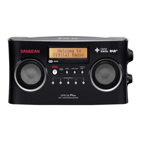
DPR-25
DAB+FM RDS+MW DIGTAL RECEVIER
CONTENTS
Specification .....................................................................................................................2-5
Block Diagram .....................................................................................................................6
Alignment Instructions..........................................................................................................7-11
Test Points Disgram.................................................................................................................12
Main PCB Top View.................................................................................................................13
Main PCB Bottom View..............................................................................................................14
LCD PCB Top View..............................................................................................................15
LCD PCB Bottom View.........................................................................................................16
PCB Top View.................................................................................................................17
PCB Bottom View.................................................................................................................18
Wiring Diagram............................................................................................................19
Troubleshooting Flow Chart.....................................................................................................20-21
Electrical Parts List.............................................................................................................22-25
Mechanical Parts List............................................................................................................26-27
Exploded Views........................................................................................................................28
IC Circuit Block Diagram......................................................................................................29-38
IC and Transistor Voltage Chart..............................................................................................39-43
Semiconductor Lead Identifications...........................................................................................44
MAIN Schematic Diagram.........................................................................................................45
LCD Schematic Diagram....................................................................................................... ...46
Advertisement
Table of Contents

Related Manuals for Sangean DPR-25


Summary of Contents for Sangean DPR-25
-
Page 1: Table Of Contents
DPR-25 DAB+FM RDS+MW DIGTAL RECEVIER CONTENTS Specification ………………………………………………………………………………………………………2-5 Block Diagram ………………………………………………………………………………………………………6 Alignment Instructions…………………………………………………………………………….………………7-11 Test Points Disgram…………………………………………………………………………….……….……………12 Main PCB Top View…………………………………………………………………………….……….……………13 Main PCB Bottom View.………………………………………………………………………….……..………..…..14 LCD PCB Top View……………………………………………………………………………….………….……15 LCD PCB Bottom View……………………………………………………………………………………………16 PCB Top View…………………………………………………………………………….……….……………17 PCB Bottom View…………………………………………………………………………….……….……………18 Wiring Diagram..….………………………………………….………………….….……………..……….19 Troubleshooting Flow Chart..….………………………………………….……………….….……………..……20-21... -
Page 2: Specification
SPECIFICA TION FM. ELECTRICAL PERFORMANCE Brand:SANGEN Temp: ¢ X C R.H.: Model: DPR-25 Date: 2005/9/2 Condition Value Test no. Test Item Unit Input Output freq Nom. 87.5 Tuning Range S/N=6dB ¡ Ó 0.05 Intermediate freq. S/N=6dB 10.7 90MHz Max. Sensitivity... - Page 3 SPECIFICA TION. MW. ELECTRICAL PERFORMANCE Temp: ¢ X C R.H.: Model: DPR-25 Date: 2005/9/2 Brand: SANGEAN Condition Value Test no. Test Item Unit Input Output freq Nom. Tuning Range 1710 ¡ Ó 2 Intermediate freq. S/N=6dB 603KHz Max. Sensitivity S/N=6dB...
- Page 4 SPECIFICATION. DAB(BAND ¢ » ) ELECTRICAL PERFORMANCE Temp: ¢ X C R.H.: Model: DPR-25 Brand: SANGEAN Date: 2005/9/2 Test no. Test Item Condition Limit Typical Unit RF Freq. Range Fc : -70 dBm (Wanted channel) Fi : ¡ Ù -38 dBm...
- Page 5 SPECIFICTION. AUX-IN ELECTRICAL PERFORMANCE Model: DPR-25 Temp: 25 ¢ J Brand: ALL R. H. : 75 % Date: 2005/9/2 Condition Value Test No. Test Item Unit Input Output Freq. Nom. Lim. AUX IN=0.5V/1KHz Output Power THD=10% Output=R.0 (ATT=0) AUX IN...
-
Page 6: Block Diagram
BLOCK DIAGRAM... -
Page 7: Alignment Instructions
ALIGNMENT INSTRUCTIONS 1. ALIGNMENT FOR AM/LW IF a. Required Instruments: AM IF Sweep Generator with scope b. Alignment Procedure Mode Adjustment Procedure (1) Press the power button to turn on the radio. (2) Connect the input terminal of AM IF sweep generator in series with a resistor of 1.2KΩ to the TP1 and TP2. - Page 8 2. ALIGNMENT FOR AM/LW TUNING VOLTAGE RANGE a. Required Instruments: b. Alignment Procedure Mode Adjustment Procedure (1) Turn on the radio. (2) Connect the probe of DVM to the test point TP1 and TP2. (3) Tune the AM frequency to 522 kHz. (4) Adjust L3 to have a reading of 1.2 0.04V.
- Page 9 3. ALIGNMENT FOR FM TUNING VOLTAGE a. Required Instruments b. Alignment Procedure Mode Adjustment Procedure (1) Turn on the radio. (2) Connect the probe of DVM to the TP1 and TP2 (3) Tune the FM frequency to 108MHz. (4) Adjust L4 to have a reading of 8.2V 0.3V. c.
- Page 10 4. ALIGNMENT FOR AM/LW SENSITIVITY a. Required Instruments AM Signal Generator SSVM b. Alignment Procedure Mode Adjustment Procedure (1) Turn on the radio. (2) Connect a SSVM to the speaker TP7 and TP8 terminals. (3) Connect an AM signal generator together with standard loop dummy antenna and feed 30% modulated signal to the AM ferrite bar antenna L12.
- Page 11 5. ALIGNMENT FOR FM TUNING SENSITIVITY a. Required Instruments FM Signal Generator (frequency range up to 220 MHz) SSVM b. Alignment Procedure Mode Adjustment Procedure (1) Turn on radio. (2) Connect a SSVM to speaker TP7 and TP8. (3) Connect a FM signal generator to TP10 and TP11. (4) Set the signal generator to 22.5 kHz deviation with 1 kHz modulation.
-
Page 12: Test Points Disgram
TEST POINTS DIAGRAM... -
Page 13: Main Pcb Top View
MAIN PCB TOP VIEW... -
Page 14: Main Pcb Bottom View
MAIN PCB BOTTOM VIEW... -
Page 15: Lcd Pcb Top View
LCD PCB TOP VIEW... -
Page 16: Lcd Pcb Bottom View
LCD PCB BOTTOM VIEW... -
Page 17: Pcb Top View
PCB TOP VIEW... -
Page 18: Pcb Bottom View
PCB BOTTOM VIEW... -
Page 19: Wiring Diagram
WIRING DIAGRAM... -
Page 20: Troubleshooting Flow Chart
TROUBLESHOOTING FLOW CHART ( 1 ) DAB can not be turned on Check the IC10 and Q14 circuit is Check whether the pin 18 of DAB normal. MODULE exceeds 3.3V DC. Then replace the abnormal parts. Check the IC13 and Q25 circuit is Check whether the pin1 of DAB normal. - Page 21 ( 3 ) Weak sensitivity in FM Check whether the sensitivity is Check the antenna wire and BPF recovered if antenna is directly circuit. connected to the pin 2 of IC12. Then replace the abnormal parts. Check whether the IF waveform is Check the IC12 circuit.
-
Page 22: Electrical Parts List
L 1,2,5,6,12, 1210360 TC 20P RED TC 1-3, 1316125 VR 50KBx2 VR 600, 1600700 LCD DPR-25 1613210 PCB D DPR-25 PCB D 1613222 PCB A DPR-25 PCB A 1613231 PCB E DPR-25 PCB E 1621011-A/10-A SPK 2.5" 8Ω 3W SP 300,301, 1630191 SW. - Page 23 ROTARY ENCODER EN 200, 1900360 W/SPK 200(6+2P) W 301, 1900830-A W/SPK 300(6+2P) R/B W 302, 1900841 DAB/M FS2020 DPR-25 MODULE 1, 4110261C CC 102K 50V Y5P 05 C 184, 442256PT0 EL 225M 50V 5x11 C 154, 443356NT0 EL 335M 50V 4x7...
- Page 24 ELECTRICAL PARTS LIST DPR-25 PART NO DESCRIPTION Q'TY REMARK 159,161,175-179,501- 504, 5010471 CH CC 104Z 25V Y5V-C C 1,2,6,12,16,19-22,25 ,27,51,54,70,72,74, 75,82,88,93,105,106, -108,111,112,124,128 130,136,151,152,158, 163,164,180,303,500, 5010557 CH CC 105Z 10V F-C C 45,46,96,155, 5012361 CH CC 123K 50V X7R-C C 77,78,...
- Page 25 ELECTRICAL PARTS LIST DPR-25 PART NO DESCRIPTION Q'TY REMARK 610014D CH RD 1/16W 4.3KJ-C R 87, 6100150 CH RD 1/16W 15KJ-C R 60,61,82,130, 6100152 CH RD 1/16W 22KJ-C R 54,92,94,144, 6100154 CH RD 1/16W 33KJ-C R 301,303, 6100156 CH RD 1/16W 47KJ-C...
-
Page 26: Mechanical Parts List
MECHANICAL PARTS LIST DPR-25 Ref no PART NO. DESCRIPTION Q'TY DWG NO. REMARK 20P4000 RUBBER KEY HOLDER A3-DPR25-01 20P4010 LCD LENS HOLDER A3-DPR25-02 20P4020 LCD LIGHT LENS A3-DPR25-03 20P4030 LED HOLDER A3-DPR25-04 « ~ © T LED-11T 20P4040 SPEAKER HOLDER-L... - Page 27 MECHANICAL PARTS LIST DPR-25 Ref no PART NO. DESCRIPTION Q'TY DWG NO. REMARK A-PCB/FRONT CABx3 BATT.CASE-2/BACK COV ERx6 FRONT CAB/MODULEx1 9163052 SCREW PTB M3x5(NI) SPK/SPK HOLDERx8 SPK HPLDER/FRONT CAB 9901030 WASHER φ3.3xφ8x0.5T...
-
Page 29: Ic Circuit Block Diagram
IC CIRCUIT BLOCK DIAGRAM 1. IC1 – TC9257FG 2. IC2 – XC6203E502PR... - Page 30 3. IC3 – TMP87EP26F...
- Page 31 4. IC4 – BU1924F 5. IC5 – NJM4556LD...
- Page 32 6. IC6 – AN7141 7. IC7 – 74HC74...
- Page 33 8. IC8 – 74HC14 9. IC9 – PT2386...
- Page 34 10. IC10 – XC6365A333MR 11. IC11 – 6002P...
- Page 35 12. IC12 – TA2149BFN 13. IC13 – XC6365A503MR...
- Page 36 14. IC14 – TC4013BFN 15. IC15 – BA09FB...
- Page 37 16. IC16 – 74AHC1G32GW 17. IC300 – TC4066BP...
- Page 38 18. IC500 – ST7066U 19. IC501 – ST7065C...
-
Page 39: Ic And Transistor Voltage Chart
IC AND TRANSISTOR VOLTAGE CHART IC1 – TC9257 IC2 – 6002PC 2.96 2.70 5.05 5.06 5.06 2.93 2.93 5.76 5.79 8.12 8.26 8.28 5.06 5.10 2.88 2.92 5.06 5.10 2.86 2.88 0.89 0.37 5.67 0.35 0.90 5.77 0.94 0.94 IC4 – BU1924 IC5 –... - Page 40 IC3 – TMP87EP26F 2.33 4.57 4.54 4.57 3.17 2.35 2.28 2.29 2.04 2.04 2.06 3.17 4.95 4.96 4.47 4.45 4.47 3.17 3.17 2.23 2.23 2.24 4.95 4.96 1.79 1.76 1.77 3.17 4.95 4.96 4.91 4.95 4.96 4.17 4.95 4.96 0.22 0.36 0.29 4.94...
- Page 41 IC7 – 74HC74 IC10 – XC6365A333MR 4.95 4.95 4.72 8.08 8.12 3.34 4.95 7.84 8.08 8.12 0.45 4.95 0.46 4.51 4.92 0.43 3.34 0.45 0.40 4.95 IC11 – 6002PC IC8 – 74HC14 7.96 8.08 8.12 4.92 4.95 6.03 6.01 6.02 0.45 4.95 4.95...
- Page 42 IC12 – TA2149BFN IC16 – 74AHC1G32GW 5.05 4.99 4.99 4.99 0.79 5.21 4.98 4.98 1.15 0.70 0.71 5.73 5.95 1.09 1.18 4.70 4.71 5.96 5.98 0.75 0.94 4.73 4.74 5.42 5.31 4.41 4.40 5.96 5.98 5.15 5.24 5.96 5.98 0.80 0.44 5.96 5.98...
- Page 43 Transistor 0.53 0.56 1.93 4.95 4.37 4.85 4.84 4.84 0.53 0.56 0.92 0.96 1.93 4.95 4.37 0.40 0.94 8.05 8.22 8.26 7.34 7.52 7.56 3.29 0.41 8.01 8.20 8.25 7.85 8.07 8.11 0.61 5.13 8.07 8.12 0.59 4.74 3.46 5.04 4.81 4.79 4.82...
-
Page 44: Semiconductor Lead Identifications
SEMICONDUCTOR LEAD IDENTIFICATIONS Transistors 2SC4154 2SB1386Q 2SA1611 2SB815 (E:Emitter C:Collector B:Base) Diodes MM4148 KV1610S 1SS314 KV1450 1SS367 ZENER RD15 IN5817 ZENER RD5.1 (A:Anode C:Cathode) -
Page 45: Main Schematic Diagram
MAIN SCHEMATIC DIAGRAM... -
Page 46: Lcd Schematic Diagram
LCD SCHEMATIC DIAGRAM...