Table of Contents
Advertisement
Quick Links
USER'S MANUAL
¯ Support Intel Pentium, MMX, Cyrix/IBM 6x86MX, MII, AMD K6,
K6-2, K6-III, IDT Winchip 2, IDT Winchip 3 & RISE MP6 CPUs.
¯ Support parity check or ECC function.
¯ Support fully AGP 1.0 specification.
¯ Support switching mode voltage regulator on board (1.3V~3.5V).
¯ Support 66/75/83/95 MHz and 100MHz.
¯ Support Modem Ring On (COMA¡ A B ) , Win 95/98 shutdown.
¯ Support Wake on Lan (The ATX power supply supports larger
than 720 mA 5V Stand-By current ).
¯ Support keyboard power on function (The ATX power
supply supports larger than 300mA 5V Stand-by current).
¯
Support Ultra DMA33 and ATA66.
¯
Support IrDA function for Fast IrDA.
Pentium
Processor PCI - ISA BUS MAINBOARD
5AA
REV. 3.2 First Edition
R-32-01-091202
Advertisement
Table of Contents

Related Manuals for Gigabyte 5AA

Summary of Contents for Gigabyte 5AA
- Page 1 USER'S MANUAL ¯ Support Intel Pentium, MMX, Cyrix/IBM 6x86MX, MII, AMD K6, K6-2, K6-III, IDT Winchip 2, IDT Winchip 3 & RISE MP6 CPUs. ¯ Support parity check or ECC function. ¯ Support fully AGP 1.0 specification. ¯ Support switching mode voltage regulator on board (1.3V~3.5V). ¯...
- Page 3 The author assumes no responsibility for any errors or omissions which may appear in this document nor does it make a commitment to update the information contained herein. ¯THIRD-PARTY BRANDS AND NAMES ARE THE PROPERTY OF THEIR RESPECTIVE OWNERS. Dec. 2, 1999 Taipei, Taiwan...
- Page 4 Quick Installation Guide CPU Jumper Setting Table: O: ON X: OFF 1.3V 2.5V 1.4V 2.6V 1.5V 2.7V 1.6V 2.8V 1.7V 2.9V 1.8V 3.0V 1.9V 3.1V 2.0V 3.2V 2.1V 3.3V 2.2V 3.4V 2.3V 3.5V 2.4V X1.5 X2.5 X3.5 X4.5 X5.5...
- Page 5 JP14 JP16 100M 105M 110M 115M 120M 125M 130M 135M 140M Note: It’s strongly recommended that set the system speed according to your hardware configuration: CPU, SDRAM, Cards, etc.
-
Page 6: Quick Installation Guide
Quick Installation Guide Quick Installation Guide: O : ON X : OFF S1 S2 S3 S4 S5 S6 S7 S8 JP14 JP16 2-3 2-3 2-3 1. Pentium 133 MHz 2-3 2-3 2-3 2. Pentium 166 MHz 2-3 2-3 2-3 3. Pentium 200 MHz 2-3 2-3 2-3 4. - Page 7 26. AMD-K6-2/550 (100*5.5 2.2V) 1-2 1-2 2-3 1-2 1-2 2-3 27. AMD-K6-III/400 (100*4 2.2V) S1 S2 S3 S4 S5 S6 S7 S8 JP14 JP16 1-2 1-2 2-3 28. AMD-K6-III/400 (100*4 2.4V) 29.AMD-K6-III/450 (100*4.5 2.2V) 1-2 1-2 2-3 30.AMD-K6-III/450 (100*4.5 2.4V) 1-2 1-2 2-3 1-2 1-2 2-3 31.
- Page 8 Quick Installation Guide º - PR333 48. Cyrix M¢ 1-2 2-3 2-3 (75*3.5 2.9V) º - PR366 49. Cyrix M¢ 1-2 1-2 2-3 (100*2.5 2.9V) º - PR366 50. Cyrix M¢ 1-2 2-3 2-3 (75*4 2.9V) S1 S2 S3 S4 S5 S6 S7 S8 JP14 JP16 º...
-
Page 9: Pentium Processor 133 Mhz
1. Pentium Processor 133 MHz M1543C JP14 JP1 JP2 M1542 JP16 2. Pentium Processor 166 MHz JP14 JP16 3. Pentium Processor 200 MHz JP14 JP16... - Page 10 Quick Installation Guide 4. Intel MMX-166 MHz JP14 JP16 5. Intel MMX-200 MHz JP14 JP16 6. Intel MMX-233 MHz JP14 JP16 7. AMD-K6/166 (2.9V) JP14 JP16 8. AMD-K6/200 (2.9V)
- Page 11 JP14 JP16 9. AMD-K6/233 (3.2V) JP14 JP16 10. AMD-K6/233 (66*3.5 2.2V) JP14 JP16 11. AMD-K6/266 (66*4 2.2V); AMD-K6-2/266 (66*4 2.2V) JP14 JP16 12. AMD-K6/300 (66*4.5 2.2V) JP14 JP16 13. AMD-K6/300 (100*3 2.2V); AMD-K6-2/300 (100*3 2.2V)
- Page 12 Quick Installation Guide JP14 JP16 14. AMD-K6-2/333 (66*5 2.2V) JP14 JP16 15. AMD-K6-2/333 (95*3.5 2.2V) JP14 JP16 16. AMD-K6-2/350 (100*3.5 2.2V) JP14 JP16 17. AMD-K6-2/366 (66*5.5 2.2V) JP14 JP16...
- Page 13 18. AMD-K6-2/380 (95*4 2.2V) JP14 JP16 19. AMD-K6-2/400 (100*4 2.2V) JP14 JP16 20. AMD-K6-2/450 (100*4.5 2.2V) JP14 JP16 21. AMD-K6-2/450 (100*4.5 2.4V) JP14 JP16 22. AMD-K6-2/475 (95*5 2.2V) JP14 JP16...
- Page 14 Quick Installation Guide 23. AMD-K6-2/475 (95*5 2.4V) JP14 JP16 24. AMD-K6-2/500 (100*5 2.2V) JP14 JP16 25. AMD-K6-2/500 (100*5 2.4V) JP14 JP16 26. AMD-K6-2/550 (100*5.5 2.2V) JP14 JP16 27. AMD-K6-III/400 (100*4 2.2V) JP14 JP16...
- Page 15 28. AMD-K6-III/400 (100*4 2.4V) JP14 JP16 29. AMD-K6-III/450 (100*4.5 2.2V) JP14 JP16 30. AMD-K6-III/450 (100*4.5 2.4V) JP14 JP16 31. AMD-K6-III/475 (95*5 2.2V) JP14 JP16 32. AMD-K6-III/475 (95*5 2.4V) JP14 JP16...
- Page 16 Quick Installation Guide 33. AMD-K6-III/500 (100*5 2.2V) JP14 JP16 34. AMD-K6-III/500 (100*5 2.4V) JP14 JP16 35. AMD-K6-III/550 (100*5.5 2.2V) JP14 JP16 36. Cyrix /IBM 6x86MX-PR166 (66*2 2.9V) JP14 JP16 37. Cyrix /IBM 6x86MX-PR200 (66*2.5 2.9V)
- Page 17 JP14 JP16 38. Cyrix /IBM 6x86MX-PR200 (75*2 2.9V) JP14 JP16 39. Cyrix /IBM 6x86MX-PR233 (66*3 2.9V) JP14 JP16 40. Cyrix /IBM 6x86MX-PR233 (75*2.5 2.9V) JP14 JP16 41. Cyrix /IBM 6x86MX-PR233 (83*2 2.9V) JP14 JP16 42. Cyrix /IBM 6x86MX-PR266 (66*3.5 2.9V)
- Page 18 Quick Installation Guide JP14 JP16 43. Cyrix / IBM 6x86MX-PR266 (75*3 2.9V) JP14 JP16 44. Cyrix / IBM 6x86MX-PR266 (83*2.5 2.9V) JP14 JP16 45. Cyrix MII-PR300 (66*3.5 2.9V) JP14 JP16 46. Cyrix MII-PR333 (66*4 2.9V) JP14 JP16 47. Cyrix M¢ º - PR333 (83*3 2.9V)
- Page 19 JP14 JP16 48. Cyrix M¢ º - PR333 (75*3.5 2.9V) JP14 JP16 49. Cyrix MII-PR333 (100*2.5 2.9V) JP14 JP16 50. Cyrix MII-PR366 (75*4 2.9V) JP14 JP16 51. Cyrix MII-PR366 (83*3.5 2.9V) JP14 JP16 52. Cyrix MII-PR400 (100*3.5 2.9V)
- Page 20 Quick Installation Guide JP14 JP16 53. IDT Winchip 2-200 (66*3 3.5V) JP14 JP16 54. IDT Winchip 2-200 (100*2 3.5V) JP14 JP16 55. IDT Winchip 2-225 (75*3 3.5V) JP14 JP16 56. IDT Winchip 2-233 (66*3.5 3.5V) JP14 JP16 57. IDT Winchip 2-233 (100*2.33 3.5V)
- Page 21 JP14 JP16 58. IDT Winchip 2-266 (66*4 3.5V) JP14 JP16 59. IDT Winchip 2-266 (100*2.66 3.5V) JP14 JP16 60. IDT Winchip 2-300 (100*2.5 3.5V) JP14 JP16 61. IDT Winchip 3-266 (100*2.33 2.8V) JP14 JP16 62. RISE MP6-266 (100*2 2.8V)
- Page 22 Quick Installation Guide JP14 JP16 III. Quick Installation Guide of Jumper setting: PWR : Power LED Connector Pin No. Function M1543C M1542 SPK : Speaker Connector...
- Page 23 Pin No. Function M1543C Signal M1542 TD : Turbo LED Connector Pin No. Function M1543C LED anode (+) LED cathode( ) M1542 TB : Turbo Switch Connector...
- Page 24 Quick Installation Guide Pin No. Function M1543C Signal M1542 RST : Reset Switch Open : M1543C Normal operation Close : Reset system M1542 GD : Green LED...
- Page 25 Pin No. Function M1543C LED anode (+) LED cathode( ) M1542 GN : Green Function Switch Open : M1543C Normal operation Close : Entering Green Mode M1542 HD : IDE Hard Disk Active LED...
- Page 26 Quick Installation Guide Pin No. Function M1543C LED anode (+) LED cathode( ) LED cathode( ) LED anode (+) M1542 Soft PWR : Soft Power Connector Open: M1543C Normal Operation Short: Power On/Off M1542 JP6: Wake On Lan...
- Page 27 M1543C Pin No. Function Signal M1542 JP7: Keyboard Power On (for ATX Power Supply only) M1543C 1-2 Close : Enable Keyboard Power On M1542 2-3 Close : Disable Keyboard Power On IDE1: Primary IDE Port...
- Page 28 Quick Installation Guide M1543C M1542 IDE2: Secondary IDE Port M1543C M1542 FLOPPY : Floppy Port...
- Page 29 M1543C M1542 LPT : LPT Port M1543C M1542 COM A : COM A Port...
- Page 30 Quick Installation Guide M1543C M1542 COM B: COM B Port M1543C M1542 USB : USB Port...
- Page 31 M1543C Pin No. Function USB D0 USB D0+ USB D1 M1542 USB D1+ JP9 : PS/2 Mouse Connector M1543C M1542 RED LINE JP9-1 : PS / 2 Mouse Connector (Optional)
- Page 32 Quick Installation Guide M1543C PS / 2 MOUSE Pin No. Function Key Data VCC (+5V) M1542 Key Clock JP10 : AT Keyboard Connector M1543C Keyboard Pin No. Function Key Clock Key Data M1542 JP10-1 : PS/2 Keyboard Connector (Optional)
- Page 33 M1543C Keyboard Pin No. Function Key Data VCC (+5V) M1542 Key Clock JP5 : AT Power Connector Pin No. Function M1543C Power Good 2,10,11,12 +12V 5,6,7,8 M1542 J1 : ATX Power Connector...
- Page 34 Quick Installation Guide Pin No. Function 3,5,7,13, 15-17 M1543C 1,2,11 3.3V 4,6,19,20 VCC (+5V) +12V Power Good 5V SB (Stand by +5V) PS-ON (Soft ON/OFF) M1542 JP4:CPU Cooling Fan Power Connector M1543C Pin No. Function +12V Signal M1542...
- Page 35 JP17 : Infrared Connector (Support FIR) M1543C Pin No. Function Power + IR Data Input IR Data Output Over Current M1542 BAT1 : For Battery M1543C – M1542 MDanger of explosion if battery is incorrectly replaced.
- Page 36 Quick Installation Guide MReplace only with the same or equivalent type recommended by the manufacturer. MDispose of used batteries according to the manufacturer’s instructions. III. Top Performance Test Setting: Users have to modify the value for each item in chipset features as follow for top performance setting.
- Page 37 Each value of items as above depends on your hardware configuration : CPU , SDRAM , Cards , etc. Please modify each value of items If your system does not work properly.
- Page 38 Quick Installation Guide PERFORMANCE LIST The following list of performance data is the testing results of some popular benchmark testing programs. These data are just referred by users, and there is no responsibility for different testing data values gotten by users. (The different Hardware & Software configuration will result in different benchmark testing results.) AMD K6-2 500, AMD K6-III 450, AMD K6-2+/450 DRAM...
-
Page 39: Table Of Contents
Table Of Contents TABLE OF CONTENTS INTRODUCTION 1.1. PREFACE ................. 1-1 1.2. KEY FEATURES ............... 1-1 1.3. PERFORMANCE LIST .............. 1-3 1.4. BLOCK DIAGRAM..............1-4 1.5. INTRODUCE THE PCI - BUS ............ 1-5 1.6. FEATURES ................1-5 1.7. What is AGP ................1-6 SPECIFICATION 2.1. - Page 40 3.11. GREEN FUNCTION INSTALLATION ........3-8 3.12. PERIPHERAL DEVICE INSTALLATION........3-8 BIOS CONFIGURATION 4.1. ENTERING SETUP ..............4-1 4.2. CONTROL KEYS ..............4-2 4.3. GETTING HELP ................ 4-3 4.3.1. Main Menu................4-3 4.3.2. Status Page Setup Menu / Option Page Setup Menu ....4-3 4.4.
-
Page 41: Introduction
Introduction 1. INTRODUCTION 1.1. PREFACE Welcome to use the 5AA motherboard. The motherboard is a Pipeline 512 KB CACHE Pentium Processor based PC / AT compatible system with ISA bus and PCI Local Bus, and has been designed to be the fastest PC / AT system. There are some new features allow you to operate the system with the performance you want. - Page 42 Supports 3*168 pin 64/72 Bit DIMM module. Supports 2-channel Enhanced PCI IDE ports for 4 IDE Devices. Supports 2*COM (16550), 1*LPT (EPP / ECP), 1*1.44MB Floppy port. Supports Green function, Plug & Play function. Licensed AMI BIOS, FLASH ROM for BIOS update. 22cm*21cm, Baby AT Form factor.
-
Page 43: Performance List
Introduction 1.3. PERFORMANCE LIST The following list of performance data is the testing results of some popular benchmark testing programs. These data are just referred by users, and there is no responsibility for different testing data values gotten by users. (The different Hardware & Software configuration will result in different benchmark testing results.) AMD K6-2 500, AMD K6-III 450, AMD K6-2+/450 DRAM... -
Page 44: Block Diagram
1.4. BLOCK DIAGRAM 100MHz 100MHz PBSRAM Host Address Host Data 100MHz MD Bus 66MHz 33MHz MA Bus DRAM 100MHz 100MHz M1542 DEVICE 66MHz 66MHz Device PCI Bus 14.318Hz Device ICS9148 33MHz AF-75 14.318Hz Device GPIO PS/2 33MHz M1543C Keyboard 48MHz Mouse Device IDE DEVICE... -
Page 45: Introduce The Pci - Bus
Introduction 1.5. INTRODUCE THE PCI - BUS Connecting devices to a CPU local bus can dramatically increase the speed of I/O- bound peripherals with only a slight increase in cost over traditional systems. This price / Performance point has created a vast market potential for local bus products. -
Page 46: What Is Agp
1.7. What is AGP The Accelerated Graphics Port (AGP) is a new port on the Host-To-PCI bridge device that supports graphics display interface. The main purpose of the AGP port is to provide fast access to system memory. The AGP port can be used either as fast PCI port (32-bits at 66MHz vs. 32-bits at 33MHz) or as an AGP port which supports 2x data-rate, a read queue, and side band addressing. -
Page 47: Specification
Specification 2. SPECIFICATION 2.1. HARDWARE Pentium Processor 133 / 166 / 200 MHz ; MMX(166 / 200 / 233) K6 (166 / 200 / 233 / 266 / 300) K6-2 (266 / 300 / 333 / 350 / 366 / 380 / 400 / 450 / 475 / 500 / 550) K6-III (400 / 450 / 475 / 500 / 550) Cyrix / IBM... -
Page 48: Software
2-channel Enhanced IDE port on board.(Using IDE PORTS IRQ14,15) Supports Mode 3,4 IDE & ATAPI CD – ROM. Supports Ultra DMA 33 and ATA 66. Supports 2 x16550 COM ports. (Using IRQ4, 3) I/O PORTS Supports 1 x SPP/EPP/ECP LPT port. (Using IRQ7 or 5 and DMA3 or 1) Supports 1 x 1.44/2.88 MB Floppy port. -
Page 49: Hardware Installation
Hardware Installation 3. HARDWARE INSTALLATION 3.1. UNPACKING The mainboard package should contain the following: The 5AA mainboard. USER’S MANUAL for mainboard. Cable set for IDE ¡B Floppy ¡B I/O Port & PS/2 mouse (Optional). CD for Mainboard Drivers and Utilities. -
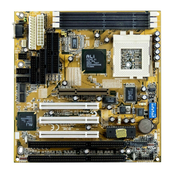
Page 50: Mainboard Layout
3.2. MAINBOARD LAYOUT ISA 2 JP17 ISA 1 BIOS PCI 3 BAT 1 M1543C PCI 2 PCI 1 COM A COM B JP16 M1542 BANK 2 BANK 1 BANK 0 ×Figure 3.1Ø Optional : ISA 2 JP17 ISA 1 PCI 3 BIOS BAT 1 M1543C... -
Page 51: Quick Reference For Jumpers & Connectors
Hardware Installation 3.3. QUICK REFERENCE FOR JUMPERS & CONNECTORS I/O Port Connectors IDE 1 Primary IDE Port. IDE 2 Secondary IDE Port. FLOPPY Floppy Port. USB Port. COM B Serial Port2 (COM B) COM A Serial Port1 (COM A). LPT Port. PS/2 PS/2 Mouse &... - Page 52 TB : Turbo Switch Connector Pin No. Function Signal RST : Reset Switch Open Normal operation Close Reset system GD : Green LED Connector Pin No. Function LED anode (+) LED cathode ( ) GN : Green Switch Open Normal operation Close Enter Green Mode HD : Hard Disk Active LED (HD-LED)
-
Page 53: Dram Installation
Hardware Installation FAN Power : CPU Cooling FAN Power Connector Pin No. Function +12V Signal JP7: Keyboard Power On Connector Pin No. Function 1,2 Close Enabled Keyboard power on. 2,3 Close Disabled Keyboard power on. JP17: Infrared Connector Pin No. Function Power + IR Data Input... -
Page 54: Cpu Installation And Jumpers Setup
socket at Vertical angle. If there is a wrong direction of Pin 1, the DRAM DIMM module couldn't be inserted into socket completely 3.6. CPU INSTALLATION AND JUMPERS SETUP The system speed depends on the frequency of CLOCK GENERATOR. The user can change SW selection to set up the system speed to 66 / 75 /83 /95 100MHz for 3.3V/2.5V Pentium Processor (133 / 166 / 200 MHz) ;MMX(166 / 200 / 233 MHZ) ,... -
Page 55: Cmos Rtc & Isa Cfg Cmos Sram
Hardware Installation X1.5 X2.5 X3.5 X4.5 X5.5 JP14 JP16 100M 105M 110M 115M 120M 125M 130M 135M 140M Note: It’s strongly recommended that set the system speed according to your hardware configuration: CPU, SDRAM, Cards, etc. Note: If Cyrix 6x86 is being used, please check the CPU Date Code after 605. 3.7. -
Page 56: Acpi Led Connector Installation
used to connect speaker. The speaker can work well in both direction of connector when it is installed to the connector SPK on mainboard. 3.9. ACPI LED CONNECTOR INSTALLATION This mainboard uses the existing power LED as ACPI LED .The ACPI LED will light on when system is power-on .The ACPI LED is off when the system is power-off. -
Page 58: Bios Configuration
BIOS Configuration BIOS CONFIGURATION AMI's BIOS ROM has a built-in Setup program that allows users to modify the basic system configuration. This type of information is stored in battery-backed CMOS RAM so that it retains the Setup information when the power is turned off. 4.1. -
Page 59: Control Keys
4.2. CONTROL KEYS Up arrow Move to previous item. Down arrow Move to next item. Left arrow Move to the item in the left hand. Right arrow Move to the item in the right hand. Esc key Main Menu - Quit and not save changes into CMOS Status Page Setup Menu and Option Page Setup Menu - Exit current page and return to Main Menu. -
Page 60: Getting Help
BIOS Configuration 4.3. GETTING HELP 4.3.1. Main Menu The on-line description of the highlighted setup function is displayed at the bottom of the screen. 4.3.2. Status Page Setup Menu / Option Page Setup Menu Press F1 to pop up a small help window that describes the appropriate keys to use and the possible selections for the highlighted item. - Page 61 Chipset features setup This setup page includes all the items of chipset special features. Power management setup This setup page includes all the items of Green function features. PNP/PCI configuration This setup page includes all the items of PNP/PCI configuration features. Load BIOS defaults BIOS defaults indicates the most appropriate value of the system parameter which the system would be in safe configuration.
-
Page 62: Standard Cmos Setup Menu
BIOS Configuration 4.5. STANDARD CMOS SETUP MENU The items in Standard CMOS Setup Menu (Figure 4.2) are divided into 9 categories. Each category includes no, one or more than one setup items. Use the arrows to highlight the item and then use the <PgUp> or <PgDn> keys to select the value you want in each item. - Page 63 Time The time format in <hour> <minute> <second>. The time is calculated base on the 24-hour military-time clock. For example, 1 p.m. is 13:00:00. Primary HDDs / Secondary HDDs The category identify the types of hard disk from drive C to drive F 4 devices that has been installed in the computer.
- Page 64 BIOS Configuration Drive A type / Drive B type The category identify the types of floppy disk drive A or drive B that has been installed in the computer. None No floppy drive installed 360K, 5.25 in. 5-1/4 inch PC-type standard drive; 360 kilobyte capacity.
- Page 65 Expanded Memory Expanded Memory in memory defined by the Lotus / Intel / Microsoft (LIM) standard as EMS. Many standard DOS applications can not utilize memory above 640, the Expanded Memory Specification (EMS) swaps memory which not utilized by DOS with a section, or frame, so these applications can access all of the system memory.
-
Page 66: Bios Features Setup
BIOS Configuration 4.6. BIOS FEATURES SETUP Figure 4.3: BIOS Features Setup 1st / 2nd / 3rd / 4th Boot Device The default value is Floppy or LS/ZIP A: or ATAPI ZIP C: or CDROM or SCSI or NETWORK or IDE-0~IDE-3 or Disabled. Floppy Boot Device by Floppy. - Page 67 Quick Boot The default value is Disabled. Enabled Enabled Quick Boot Function. Disabled Disabled Quick Boot Function. Bootup Num-Lock Default value is On. Keypad is number keys. Keypad is arrow keys. Floppy Drive Swap The default value is Disabled. Enabled Floppy A &...
- Page 68 BIOS Configuration HDD Access Control The default value is Normal. Normal Set HDD Access Control : Normal. Read Only Set HDD Access Control : Read Only. PS/2 Mouse Support The default value is Enabled. Enabled Enabled PS/2 Mouse Support Function. Disabled Disabled PS/2 Mouse Support Function.
- Page 69 Internal Cache The default value is Enabled. Enabled Enabled Internal Cache Function. Disabled Disabled Internal Cache Function. External Cache The default value is Enabled. Enabled Enabled External Cache Function. Disabled Disabled External Cache Function. System BIOS Cacheable The default value is Disabled. Enabled Enabled System BIOS Cacheable.
-
Page 70: Chipset Features Setup
BIOS Configuration 4.7. CHIPSET FEATURES SETUP Figure 4.4: Chipset Features Setup USB Function The default value is Enabled. Enabled Enabled USB Function. Disabled Disabled USB Function. USB Legacy Support. The default value is Disabled. Enabled Enabled USB Legacy Support Function. Disabled Disabled USB Legacy Support Function. - Page 71 DRAM Data Integrity Mode The default value is Parity. Set DRAM Data Integrity Mode to ECCMode. Parity Set DRAM Data Integrity Mode to ParityMode. SDRAM Burst Mode The default value is Enabled. Enabled Enabled SDRAM Burst X-1-1-1-1-1-1-1. Disabled Disabled SDRAM Burst X-1-1-1-1-1-1-1. DRAM Timing The default value is Normal.
- Page 72 BIOS Configuration Graphics Aperture Size The default value is 64MB. Set Graphics Aperture Size to 4MB. Set Graphics Aperture Size to 8MB. 16MB Set Graphics Aperture Size to 16MB. 32MB Set Graphics Aperture Size to 32MB. 64MB Set Graphics Aperture Size to 64MB. 128MB Set Graphics Aperture Size to 128MB.
- Page 73 Passive Release The default value is Enabled. Enabled Enable Passive Release. Disabled Disable Passive Release. ISA Line Buffer The default value is Enabled. Enabled Enable ISA Line Buffer. Disabled Disable ISA Line Buffer. Delay Transaction The default value is Disabled. Enabled Enable Delay Transaction.
-
Page 74: Power Management Setup
BIOS Configuration Spread Spectrum The default value is Disabled. Disabled Normal. 0.6%(CNTR) Set Spread Spectrum 0.6%( Center Spread). 4.8. POWER MANAGEMENT SETUP Figure 4.5: Power Management Setup *These four items will be available when RTC Alarm Resume is set to Enabled. - Page 75 Video Power Down Mode The default value is Stand By. Disabled Disabled Video Power Down Mode Function. Stand By Set Video Power Down Mode to Stand By. Suspend Set Video Power Down Mode to Suspend. Hard Disk Power Down Mode The default value is Disabled.
- Page 76 BIOS Configuration Monitor Parallel Port The default value is Yes. Enabled Monitor Parallel Port Function. Disabled Monitor Parallel Port Function. Monitor Serial Port The default value is Yes. Enabled Monitor Serial Port Function. Disabled Monitor Serial Port Function. Monitor Floppy The default value is Yes.
- Page 77 Monitor Sec-HDD The default value is No. Enabled Monitor Sec-HDD Function. Disabled Monitor Sec-HDD Function. Power Button Function The default value is Soft Off. Soft Off Set Power Button Function to Soft Off. Suspend Set Power Button Function to Delay 4 sec. MODEM Use IRQ The default value is 3.
- Page 78 BIOS Configuration RTC Alarm Resume The default value is Disabled. Enabled Enable RTC Alarm Resume function. Disabled Disable RTC Alarm Resume function. If RTC Alarm Resume is Enabled. Date Alarm : Every Day,1~31 Hour Alarm : 0~23 Minute Alarm : 0~59 Second Alarm : 0~59...
-
Page 79: Pnp/Pci Configuration
4.9. PNP/PCI CONFIGURATION Figure 4.6: PCI Slot Configuration *These two items will be available when OffBoard PCI IDE Card is set to Slot 1. Plug and Play Aware O/S The default value is No. Enable Plug and Play Aware O/S function. Disable Plug and Play Aware O/S function. - Page 80 BIOS Configuration PCI Latency Timer The default value is 64. Set PCI Latency Timer to 32. Set PCI Latency Timer to 64. Set PCI Latency Timer to 96. Set PCI Latency Timer to 128. Set PCI Latency Timer to 160. Set PCI Latency Timer to 190.
- Page 81 OffBoard PCI IDE Pri.IRQ The default value is Disabled. Disabled Disabled OffBoard PCI IDE Pri.IRQ . INTA Set OffBoard PCI IDE Pri.IRQ to INTA. INTB Set OffBoard PCI IDE Pri.IRQ to INTB. INTC Set OffBoard PCI IDE Pri.IRQ to INTC. INTD Set OffBoard PCI IDE Pri.IRQ to INTD.
-
Page 82: Load Bios Defaults
BIOS Configuration IRQ (3,4,5,7,9,10,11,12,14,15) The default value is "ISA/EISA" or "PCI/PnP". ISA/EISA The resource is used by ISA/EISA device. PCI/PnP The resource is used by PCI/PnP device. 4.10. LOAD BIOS DEFAULTS Figure 4.7: Load BIOS Defaults Load BIOS Defaults To load BIOS defaults value to CMOS RAM, enter "Y". If not, enter "N". 4-25... -
Page 83: Load Setup Defaults
4.11. LOAD SETUP DEFAULTS Figure 4.8: Load Setup Defaults Load SETUP Defaults To load SETUP defaults value to CMOS RAM, enter "Y". If not, enter "N". If there is any problem occurred, loading BIOS DEFAULTS step is recommended. 4-26... -
Page 84: Integrated Peripherals
BIOS Configuration 4.12. INTEGRATED PERIPHERALS Figure 4.9: Integrated peripherals These two items will Enabled when OnBoard Serial Port3 is set to Enabled. **The item will Enable when Parallel Port Mode is set to ECP # These two items will show up when KeyBoard PowerOn is set to Enabled OnBoard FDC The default value is Enabled. - Page 85 OnBoard Serial Port 1 The default value is 3F8h/COM1. Auto BIOS will automatically setup the port 1 address. 3F8h/COM1 Enable OnBoard Serial port 1 and address is 3F8h. 2F8h/COM2 Enable OnBoard Serial port 1 and address is 2F8h. 3E8h/COM3 Enable OnBoard Serial port 1 and address is 3E8h. 2E8h/COM4 Enable OnBoard Serial port 1 and address is 2E8h.
- Page 86 BIOS Configuration Serial Port 3 IRQ The default value is N/A. Set Serial Port 3 IRQ to 3. Set Serial Port 3 IRQ to 4. Set Serial Port 3 IRQ to 5. Set Serial Port 3 IRQ to 9. Set Serial Port 3 IRQ to 10. Set Serial Port 3 IRQ to 11.
- Page 87 Parallel Port DMA Channel The default value is N/A. Set Parallel Port DMA Channel to 1. Set Parallel Port DMA Channel to 3. KeyBoard PowerOn The default value is Disabled. Enabled Enabled KeyBoard PowerOn. Disabled Disabled KeyBoard PowerOn. PowerOn Select The default value is N/A.
- Page 88 BIOS Configuration OnBoard IDE The default value is Both. Both Set OnBoard IDE is Both. Disabled Disabled OnBoard IDE Function. Primary Set OnBoard IDE is Primary. Secondary Set OnBoard IDE is Secondary. 4-31...
-
Page 89: Supervisor / User Password
4.13.SUPERVISOR / USER PASSWORD When you select this function, the following message will appear at the center of the screen to assist you in creating a password. Figure 4.10: Password Setting Type the password, up to eight characters, and press <Enter>. The password typed now will clear previously entered password from CMOS memory. -
Page 90: Ide Hdd Auto Detection
BIOS Configuration 4.14. IDE HDD AUTO DETECTION Figure 4.11: IDE HDD Auto Detection The screen will display the ¡ § S tandard CMOS Setup¡¨ o nce you enter the menu. User won’ t need to make any changes to items in the menu. The system will auto detect the HDD and save it in the CMOS setup menu. -
Page 91: Save & Exit Setup
4.15. SAVE & EXIT SETUP Figure 4.12: Save & Exit Setup Type "Y" will quit the Setup Utility and save the user setup value to RTC CMOS RAM. Type "N" will return to Setup Utility. 4-34... -
Page 92: Exit Without Saving
BIOS Configuration 4.16. EXIT WITHOUT SAVING Figure 4.13: Exit Without Saving Type "Y" will quit the Setup Utility without saving to RTC CMOS RAM. Type "N" will return to Setup Utility. 4-35... -
Page 94: Troubleshooting
5. Troubleshooting How to remove “?PCI Universal Serial Bus” under the Windows 95 ? Method 1: 1.Please Install Windows 95 OSR2.1 attached file “USBSUPP.EXE” 2.Run this file and then system will restart. 3.Please go to the Device Manager , and remove “?PCI Universal Serial Bus”. - Page 96 Product Name: Mother Board residential installations. This equipment Model Number: GA-5AA generates, uses, radiate radio Conforms to the following specifications: FCC Part 15, Subpart B, Section 15.107(a) and Section 15.109(a), frequency energy, and if not installed and used...
-
Page 98: Declaration Of Conformity
Ausschlager Weg 41, 1F, 20537 Hamburg, Germany declare that the product ( description of the apparatus, system, installation to which it refers) Mother Board GA-5AA is in conformity with (reference to the specification under which conformity is declared) in accordance with 89/336 EEC-EMC Directive...