Table of Contents
Advertisement
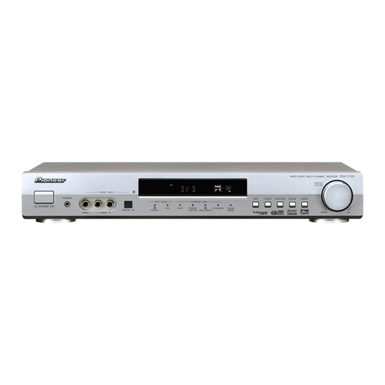
AUDIO/VIDEO MULTI-CHANNEL RECEIVER
VSX-C100-S
VSX-C100-K
THIS MANUAL IS APPLICABLE TO THE FOLLOWING MODEL(S) AND TYPE(S).
Model
Type
VSX-C100-S
MYXU
VSX-C100-K
MYXU
VSX-C100-S
NVXU
For details, refer to "Important symbols for good services" .
PIONEER CORPORATION
PIONEER ELECTRONICS (USA) INC. P.O. Box 1760, Long Beach, CA 90801-1760, U.S.A.
PIONEER EUROPE NV Haven 1087, Keetberglaan 1, 9120 Melsele, Belgium
PIONEER ELECTRONICS ASIACENTRE PTE. LTD. 253 Alexandra Road, #04-01, Singapore 159936
PIONEER CORPORATION 2002
STANDBY/ON
Power Requirement
AC220-230V
AC220-230V
AC240V
4-1, Meguro 1-chome, Meguro-ku, Tokyo 153-8654, Japan
AUDIO/ VIDEO MULTI-CHANNEL RECEIVER
MASTER
VOLUME
FRONT INPUT
PHONES
DVD
TV/SAT
DVR/VCR
FM/AM
FRONT
SURROUND MODE
INPUT SIGNAL
2
2
DTS
AUTO
PHONES
ADVANCED
SOUND
DIGITAL IN
DIGITAL
/VIRTUAL
PRO LOGIC II
MODE
R
DOWN
VIDEO
L
AUDIO
R
VSX-C100-S
VSX-C100
ORDER NO.
RRV2605
UP
Remarks
T-ZZR MAY. 2002 printed in Japan
Advertisement
Table of Contents

Related Manuals for Pioneer VSX-C100


Summary of Contents for Pioneer VSX-C100
- Page 1 PIONEER CORPORATION 4-1, Meguro 1-chome, Meguro-ku, Tokyo 153-8654, Japan PIONEER ELECTRONICS (USA) INC. P.O. Box 1760, Long Beach, CA 90801-1760, U.S.A. PIONEER EUROPE NV Haven 1087, Keetberglaan 1, 9120 Melsele, Belgium PIONEER ELECTRONICS ASIACENTRE PTE. LTD. 253 Alexandra Road, #04-01, Singapore 159936 PIONEER CORPORATION 2002 T-ZZR MAY.
-
Page 2: Safty Information
(water pipe, conduit, etc.) by connecting a leakage c u r r e n t t e s t e r s u c h a s S i m p s o n M o d e l 2 2 9 - 2 o r 2. - Page 3 Appropriately applying grease or glue can maintain the product performances. But improper lubrication or applying glue may lead to failures or troubles in the product. By following the instructions in this manual, be sure to apply the prescribed grease or glue to proper portions by the appropriate amount.For replacement parts or tools, the prescribed ones should be used.
-
Page 4: Table Of Contents
3.10 POWER(2/2) and TORANS ASSYS ........30... -
Page 5: Specifications
FM Tuner Section Continuous Power Output (STEREO MODE) Frequency Range.........87.5 MHz to 108 MHz FRONT..... 25 W + 25 W (DIN 1 kHz, THD 1 %, 8 Ω) Usable Sensitivity.....Mono:15.2 dBf, IHF (1.6 µV/ 75 Ω) 50 dB Quieting Sensitivity........Mono: 20.2 dBf Continuous Power Output (SURROUND MODE) ..........Stereo: 41.2 dBf... -
Page 6: Exploded Views And Parts List
2. EXPLODED VIEWS AND PARTS LIST NOTES: Parts marked by "NSP" are generally unavailable because they are not in our Master Spare Parts List. mark found on some component parts indicates the importance of the safety factor of the part. - Page 7 Right Pad C100 AHA7382 Speaker Cable Label ARW7163 Packing Sheet AHG7015 Spacer AHC7026 (2) CONTRAST TABLE VSX-C100-S/MYXU, /NVXU and VSX-C100-K/MYXU are constructed the same except for the following : VSX-C100-S/ VSX-C100-S/ VSX-C100-K/ Mark Symbol and Description MYXU NVXU MYXU Polyethylene Bag...
-
Page 8: Exterior Section
2.2 EXTERIOR SECTION NON-CONTACT SIDE CONTACT SIDE 8(2/4,3/4) 8 : Fan Cover_Cut diagram 8(4/4) Barrier B Fan Cover 8(1/4) Refer to "2.3 FRONT PANEL SECTION". Card Card Spacer Spacer 8(3/4) 8(2/4) Barrier A VSX-C100-S... - Page 9 VNK4840 Label C100SMY ARW7171 FFC (J003 : 7P/100BD 60V) ADD7344 (DSP CN804 to FRONT CN203) (2) CONTRAST TABLE VSX-C100-S/MYXU, /NVXU and VSX-C100-K/MYXU are constructed the same except for the following : VSX-C100-S/ VSX-C100-S/ VSX-C100-K/ Mark Symbol and Description MYXU NVXU...
-
Page 10: Front Section
2.3 FRONT SECTION VSX-C100-S... - Page 11 VOL Ring ABH7220 Volume Knob Assy See Contrast table(2) NSP 13 Power Button See Contrast table(2) (2) CONTRAST TABLE VSX-C100-S/MYXU, /NVXU and VSX-C100-K/MYXU are constructed the same except for the following : VSX-C100-S/ VSX-C100-S/ VSX-C100-K/ Mark Symbol and Description MYXU NVXU...
-
Page 12: Block Diagram And Schematic Diagram
3. BLOCK DIAGRAM AND SCHEMATIC DIAGRAM 3.1 BLOCK DIAGRAM DSP ASSY 6P JACK IC701 NJU7313AM ASSY AUDIO FUNCTION IC1401 SELECTOR NJU7313AM SP Config. MIX AMP. 2PA JACK ASSY FRONT INPUT ASSY (1/3) POWER ASSY (1/3) DIG-IN ASSY IC1101 AK4586BVQ CODEC... - Page 13 FRONT INPUT ASSY (3/3) E VOL. PRE AMP. POWER ASSY (3/3) 1103 VSX-C100-S...
-
Page 14: Overall Wiring Diagram
3.2 OVERALL WIRING DIAGRAM 1/2, POWER ASSY (AWX8042) FRONT INPUT ASSY (AWX8053) FRONT ASSY (AWX8050) SW ASSY (AWX8051) VSX-C100-S... - Page 15 VIDEO ASSY 6PA-JACK ASSY DIGITAL-IN (AWX8047) (AWX8043) ASSY (AWX8046) 1/4- DSP ASSY (AWX8049) TUNER MODULE (AXQ7232) 2PA- JACK GNDRY ASSY (AWX8048) ENCODER ASSY (AWX8052) VSX-C100-S...
-
Page 16: Fm/Am Tuner Module
3.3 FM/AM TUNER MODULE FM/AM TUNER MODULE (AXQ7232) FM FRONT END (FM) (FM) (FM) (FM) (AM) (AM) (AM) MW RF TUNING BLOCK (FM) (AM) VSX-C100-S... - Page 17 : The power supply is shown with the marked box. (TX) : AUDIO SIGNAL ROUTE (TUNER) (AM) : AM SIGNAL ROUTE (FM) : FM SIGNAL ROUTE (AM) (TX) (FM) (TX) (TX) (TX) (FM) (FM) (TX) (AM) VSX-C100-S...
-
Page 18: Dsp(1/4), 2P-Jack, 6P-Jack, Digital-In And Front Input Assys
3.4 DSP(1/4), 2P-JACK, 6P-JACK, DIGITAL-IN and FRONT INPUT ASSYS 6P JACK ASSY (AWX8043) 2PA JACK ASSY (AWX8048) Analog Function Selector DSP ASSY (AWX8049) DIGITAL-IN ASSY (AWX8046) CN3201 C D F VSX-C100-S... - Page 19 CN201 : AUDIO SIGNAL ROUTE (Analog) CN803 : AUDIO SIGNAL ROUTE (Digital) ON :4.7V OFF: 0V FRONT INPUT ASSY (AWX8053) VSX-C100-S...
-
Page 20: Dsp(2/4) Assy
3.5 DSP(2/4) ASSY DSP ASSY (AWX8048) AAC : 5V AAC Except : 0v VSX-C100-S... - Page 21 : AUDIO SIGNAL ROUTE A / D CODEC D / A VSX-C100-S...
-
Page 22: Dsp(3/4) Assy
3.6 DSP(3/4) ASSY DSP ASSY (AWX8049) (FL) (FL) (FL) (FL) (FL) (RL) (SW) (SL) (FL) (SL) (RL) (SL) (RL) (FL) SW SW (SL) (SL) (SW) (SW) (SW) (SW) DIGITAL MUTE BLOCK LPF BLOCK VSX-C100-S... - Page 23 : AUDIO SIGNAL ROUTE ( Salund L ch) : AUDIO SIGNAL ROUTE (Center) (FL) (FL) (FL) (SL) (FL) (FL) (RL) (SW) (SW) (SW) (SW) E.VOL MUTE 1.6V UN MUTE -12V : The power supply is shown with the marked box. VSX-C100-S...
-
Page 24: Dsp(4/4) Assy
3.7 DSP(4/4) ASSY DSP ASSY (AWX8048) CIRCUIT (FL) (FL) (FL) DIRECT (FL) (FR) (SL) (SL) (SL) (SL) (SW) (SL) (SR) (SR) (SW) (SW) (SW) (SW) S.BASS OFF 3.9V ON -12V (SW) (S.BASS ON Only) VSX-C100-S... - Page 25 : AUDIO SIGNAL ROUTE (FL) : AUDIO SIGNAL ROUTE (Front L ch) (SL) (FL) (FL) : AUDIO SIGNAL ROUTE (Rear L ch) (SW) : AUDIO SIGNAL ROUTE (Sub Woofer) (FL) : AUDIO SIGNAL ROUTE (Center) (SW) (SL) (SL) (FL) (SL)
-
Page 26: Front, Encoder And Sw Assys
3.8 FRONT, ENCODER and SW ASSYS FRONT ASSY (AWX8050) EXPAN DED LED : 1 to 7 5V : LED ON 0V : LED OFF VSX-C100-S... - Page 27 S4202 : TV/SAT S4203 : VCR S4204 : TUNER S4205 : FRONT TUNER SW ASSY S4501 : POWER STANDBY/ON SW ASSY (AWX8051) ENCODER ASSY : The power supply is shown with the marked box. (AWX7914) ENCODER ASSY S4401 : MASTER VOLUM VSX-C100-S...
-
Page 28: Power(1/2) Assy
3.9 POWER(1/2) ASSY POWER ASSY (AWX8042) POWER AMP BLOCK (FL) (FL) (SL) (FL) (FL) (SW) (SW) (SL) (SL) SP DETECT BLOCK FAN CONTROL BLOCK CN1601 VSX-C100-S... - Page 29 : AUDIO SIGNAL ROUTE (Sub Woofer) (FL) (FL) : AUDIO SIGNAL ROUTE (Front L ch) : AUDIO SIGNAL ROUTE (Center) (FL) (FL) SPEAKERS (SL) (SL) SPEAKERS (SL) (SL) (SL) (SL) CN4101 : The power supply is shown with the marked box. CN1601 VSX-C100-S...
-
Page 30: Power(2/2) And Torans Assys
3.10 POWER(2/2) and TORANS ASSYS POWER TRANSFORMER Secon Dary WHITE CN452 CN1602 CN451 VSX-C100-S... - Page 31 (AWX8042) REK1023 1.25A/250V BKP1046 AC IN ATT7037 0.01 • NOTE FOR FUSE REPLACEMENT CAUTION - FOR CONTINUED PROTECTION AGAINST RISK OF FIRE. REPLACE WITH SAME TYPE AND RATINGS ONLY. : The power supply is shown with the marked box. VSX-C100-S...
-
Page 32: Video Assy
3.11 VIDEO ASSY VIDEO ASSY (AWX8047) : VIDEO SIGNAL ROUTE MONITOR2 VSX-C100-S... - Page 33 VSX-C100-S...
-
Page 34: Pcb Connection Diagram
4. PCB CONNECTION DIAGRAM NOTE FOR PCB DIAGRAMS : 1. Part numbers in PCB diagrams match those in the schematic 3. The parts mounted on this PCB include all necessary parts for diagrams. several destinations. 2. A comparison between the main parts of PCB and schematic For further information for respective destinations, be sure to diagrams is shown below. -
Page 35: Fm/Am Tuner Module
4.1 FM/AM TUNER MODULE SIDE B SIDE A FM/AM TUNER MODULE CN201 CN803 (ANP7338-B) Q202 FM/AM TUNER MODULE SIDE B CN201 (ANP7338-B) Q201 IC201 Q203 Q205 IC202 Q204 VSX-C100-S... -
Page 36: Dsp And 2Pa-Jack Assy
4.2 DSP and 2PA-JACK ASSY SIDE A DSP ASSY CN901 CN801 CN761 DSP ASS'Y PYKC-F4X C1106 C1105 C1104 C1103 AWX8049 C1108 C1107 CN801 AWX8062 C1110 R1114 AWX8066 C1111 R1212 C1112 C1217 AWX8071 X1101 C1216 L1103 C1123 R1106 R1113 R1107 C1142... - Page 37 SIDE A WARNING THIS PRODUCT CONTAINS LEAD IN SOLDER AND CERTAIN ELECTRICAL PARTS CONTAIN CHEMICALS WHICH ARE KNOWN TO THE STATE OF CALIFORNIA TO CAUSE CANCER, BIRTH DEFECTS OR OTHER R1263 REPRODUCTIVE HARM. HEALTH & SAFETY CODE SECTION 25249.6 - PROPOSITION 65...
-
Page 38: Dsp Assy
SIDE B DSP ASSY ATTENTION C1221 EN CAS DE REMPLACEMENT DES FUSIBLES R1240 C1222 R1239 C1223 IC1603,IC1604 N'UTILISER QUE LA R1238 C1224 R1237 REFERENCE R1236 IC1202 R1235 46101.6 DE CHEZ C1292 R1234 R1233 LITTELFUSE INC. C1264 L1202 AWX8049 AWX8062 L1204... - Page 39 R713 2PA-JACK R1321 R1309 R1310 R1333 C717 R712 ASSY R711 C1327 C1315 C1329 C1316 C1330 C1317 C1318 C1328 C 7 1 8 C847 C848 CN802 C1560 R754 R1528 R753 R701 C1559 CN2201 IC1503 C2204 C2203 R1585 R1586 CN701 C1805 R1536...
-
Page 40: Power And Front Input Assys
IC201 IC201 AWX8042 AWX8074 IC202 W121 AWX8065 GNDS AWX8068 AWX8100 W122 FANIOUT W112 FANIOUT PRIMARY J106 J108 W1001 EXCEPT L101 /B MODEL AC IN NEUTRAL J107 CN101 LIVE CN102 J104 CN101 RISK OF FIRE - REPLACE FUSE AS MARKED. VSX-C100-S... - Page 41 ACRY HP R ACWUP W148 V+5R6 V+RY -VFL W147 GNDU CN452 FLAC1 GNDRY FLAC2 C457 CN451 ANP7422- (ANP7422-B) To Transformer FRONT INPUT ASSY C4101 JA4103 CN304 JA4101 V+5OPT F-OPT VIDEO GNDOPT HPDCT GNDH C4108 FVIDEO PYKC-F4X GNDV CN4101 ANZ7139 GNDA AWX8053 N.C.
- Page 42 FTRY F452 FANIOUT C462 SROUT SRIN ACRY ACWUP V+5R6 -VFL GNDU FLAC1 FLAC2 CN452 D454 Q389 Q390 (ANP7422-B) Q387 FRONT INPUT ASSY Q201 C4109 C4102 C4117 C4110 C4104 R4107 C4111 C4119 R4104 CN4101 R4106 G.OPT HDCT GNDH VIDEO GNDV GNDA AWX8053 N.C.
- Page 43 SIDE B CN301 COMPLEX1 ASS'Y CN301 AWM7673 0 1 2 3 4 5 6 7 8 9 0 1 2 3 AWM7678 CN305 AWM7680 AWM7682 AWM7711 D401 D386 D387 Q409 Q410 D403 R313 R346 R344 C331 R345 R343 R303 R304...
-
Page 44: 6Pjack, Dig.in, Sw, Encoder And Video Assys
4.4 6PJACK, DIG.IN, SW, ENCODER and VIDEO ASSYS SIDE A FRONT ASSY CN303 J4204A J4204 CN4201 C4302 R4272 C4229 R4243 R4335 Q4205 CN4201 C4216 R4226 Q4202 C4217 C422 C4225 4201 C4214 C4208 V4301 D4209 D4210 D4205 D4201 D4206 D4207 D4208... - Page 45 SIDE A CN804 CN1702 J4401 J4205 CN4203 CN4202 CONTACT SIDE R4272 C4229 C4251 CN4203 CN4202 R4259 CONTACT SIDE R4252 R4335 C4220 R4299 R4336 C4206 X4681 R4218 C4228 C4205 Q4683 R4274 C4683 D4214 R4687 R4276 Q4681 C4682 R4229 C4211 C4684 C4242...
- Page 46 SIDE B FRONT ASSY CN4202 CN4203 R4273 J4205 C 4 3 0 4 C4690 C4689 IC4681 R4245 R4686 R4246 R4238 AWX8050 R4247 ADVANCED AWX8063 SOUNDMODE R4267 AWX8067 AWX8072 R4682 C4237 R4236 R4231 R4249 R4265 Q4682 R4264 IC4681 IC4201 Q4682 SW ASSY...
- Page 47 SIDE B CN4201 D4203 C4303 J4204 D4213 R4235 R4207 R4216 D4204 C4230 C4301 C4236 C4201 ADVANCED C4209 C4232 PHONES/VIRTUAL (AAC) C4237 AUTO R4284 C4233 R4282 PROLOGIC C4234 R4283 R4290 DOLBY DIGITAL (ANP7423-B) Q4201 VIDEO ASSY 1.VIDEO3 AWX8101 2.VIDEO2 3.VIDEO1 4.V-6V AWX8075 5.V-12...
-
Page 48: Pcb Parts List
When ordering resistors, first convert resistance values into code form as shown in the following examples. Ex.1 When there are 2 effective digits (any digit apart from 0), such as 560 ohm and 47k ohm (tolerance is shown by J=5%, and K=10%). - Page 49 C315, C316, C355 CEHAT101M35 Other Resistors RS1/16S###J C356 CEHAT101M35 OTHERS C391 CEHAT221M10 CN761 11P SOCKET KP200TA11L C307, C308, C347 CEHAT470M25 JA761 6P PIN JACK VKB1130 C348, C384 CEHAT470M25 C464 CKSQYB473K50 C393, C483 CKSRYB102K50 DIGITAL-IN ASSY C203, C204, C205 CKSRYB103K50 SEMICONDUCTORS C402, C406...
- Page 50 Q1512, Q1513, Q1514, Q1515 2SC3326 C210 CEJQ470M16 Q1516, Q1517, Q1518, Q1701 2SC3326 Q1801, Q701, Q702 2SC3326 C103, C104, C204, C238, C609 CKSRYB102K50 C102, C208, C216, C217, C220 CKSRYB103K50 Q1101, Q1262, Q1405, Q1406 DTA124EK C239, C242, C604, C610, C615 CKSRYB103K50 Q1408, Q1408, Q1503, Q1504...
- Page 51 C1101, C1102 CCSRCH220J50 C1125, C1330, C1426 CKSRYB104K25 C1112, C1142, C1290, C1292, C1527 CCSRCH221J50 C1432, C1440, C1440 CKSRYB104K25 C1528, C1533, C1534, C1541 CCSRCH221J50 C1540, CC1545, C1709, C1710, C1721 CKSRYB104K25 C1213, C1542 CCSRCH271J50 C1722, C1726 CKSRYB104K25 C1329, C1331, C793 CCSRCH331J50 C754 CKSRYB104K25 C1730...
- Page 52 C4102, C4106, C4110 CKSRYB104K25 C4683 CEJQ101M10 C4112, C4113 CKSRYB223K50 C4686 CEJQ2R2M50 C4230, C4231 CKSQYF225Z16 RESISTORS C4201, C4210, C4226, C4228, C4229 CKSRYB102K50 Other Resistors RS1/16S###J C4251, C4274, C4681, C4682 CKSRYB102K50 OTHERS C4209, C4213, C4215, C4222, C4241 CKSRYB103K50 C4205, C4206, C4207, C4211, C4220 CKSRYB104K25...
-
Page 53: Adjustment
Contents Modulation (MHz) (dBµV) point Adjust L201 so that the DC voltage between T-METER L201 Pin 21 and Pin 23 of IC201 (Test point Vtm) Adjustment gets within 0 ± 50mV. PRODUCT MPX SG FM SG Voltmeter FM75Ω antenna terminal Fig.1 Adjustment Wiring Diagram... -
Page 54: General Information
• VOL value: 0 dB FL and LED change cyclically as follows: Normal display → All lights for the FL and LED on → All lights • Distance setting for the front: 3 m for the FL and LED off → FL: "ABCDEFGH" displayed; and •... -
Page 55: Protection Of The Amplifier Line
While the unit is recovering from the abnormality, the "OVERLOAD" display continues flashing. 3. Specifications of DSP Overload Detection 1. Detect overload detection signal of DSP in the port and light a "OVER" segment if detected for 30 seconds. Light it for 1 second if lighted once. -
Page 56: Operation Of The Fan-Control Line
(110°C)204 - "OVERHEAT" flashes • If you wish to switch FAN START from "H" to "L" and FAN MAX from "L" to "H," first set FAN START to "L," then after 100 µs, set FAN MAX to "H." • While "OVERHEAT" is flashing, only the POWER key is functional. -
Page 57: Specifications Of Speaker Detection
The response signal will be read at A/D. A voltage of 3.5 V or more is judged as no speaker connected. The response signals at A/D are read every 2 ms, and if the same results (less or more than 3.5 V) are obtained, the detection result is considered correct. -
Page 58: Circuit Description
(1) When the DC voltage of the plus (+) side was generated on the SP edge When the DC voltage of the plus (+) side was generated in L ch or R ch, Q384 turns ON and DDCT becomes Low level if VB of Q384 becomes higher than operating point. -
Page 59: Trouble Shooting
(red for input) and • Check the voltage of IC1101(DSP Assy) DOLBY DIGITAL LED • Is the switch of analog / digital signal becoming with digital or AUTO? lighting? • Is input switch setting of coax and optical 1 properly ? -
Page 60: Error Code
PHONES.IN Flashes for five seconds operation button which does not accept. 7.1.8 Fan Cleaning Before shipping out the product, be sure to clean the following positions by using the prescribed cleaning tools: Position to be cleaned Cleaning tools Fans Cleaning paper : GED-008... -
Page 61: Parts
7.2 PARTS 7.2.1 IC • The information shown in the list is basic information and may not correspond exactly to that shown in the schematic diagrams. List of IC PDG269A, CS493292, BU4094BCF, NJU3712M, M62446 PDG269A (FRONT ASSY: IC4201) • Mode Control IC... - Page 62 AC pulse input RDS DT Serial control data signal for RDS communication RDS CK Serial control clock signal for RDS communication (Use for external interrupt) DLCK ERR/OVER signal input from CODEC Remote control signal input (non carrier signal) CDC DI...
- Page 63 Strobe of expansion IC (for 4094) 731* CS Chip select of NJU7311 - 7313 IATT Input ATT switch EVOL ST Strobe signal for communication with the electronic volume DSP MT DSP mute (Assy mute) EXP OE OE of expansion IC 3712 ST...
- Page 64 Data output of microcomputer SCDOUT AUDATA0 Audio data output (FL/FR) communication INTREQ Microcomputer communication request LRCLK LR clock of audio output data EXTMEM Output enable of external memory SCLK Bit clock of audio output data SDATAN1 Audio data input MCLK...
-
Page 65: Display
7.2.2 DISPLAY 7 AAV7088 (FRONT ASSY : V4301) • FL DISPLAY • Pin Assignment • Grid Assignment • Segment Designation VSX-C100-S... - Page 66 • Pin Connection • Anode Connection VSX-C100-S...
-
Page 67: Panel Facilities
Lights when the AUTO mode is selected. This mode automatically SLEEP Lights when the function is set or active . selects which kind of signal is being input and plays back in the OVER indicator appropriate mode. Lights when the analog signal is too powerful, PHONES/VIRTUAL: causing possible distortion . -
Page 68: Remote Control
MASTER VOLUME +/– buttons: Use to set the overall listening volume. MUTE button : Use to mute the sound or restore the sound if it has been muted. RECEIVER TOP MENU button: Use to return to the most basic menu on a DVD player or disc. - Page 69 Remote 2 MENU button: Use to return to the most basic menu on a DVD player or disc. Also used for some tuner commands. # } ] ’ ‘ & ENTER buttons Use these arrow buttons when adjusting the tuner or navigating TV or DVD menus.