
Related Manuals for Panasonic DMR-E85HP


Summary of Contents for Panasonic DMR-E85HP
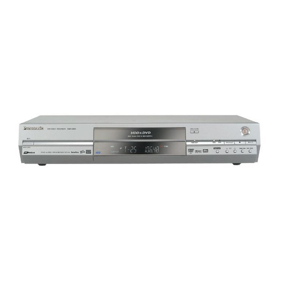
- Page 1 ORDER NO.DSD0403003C1 DVD Video Recorder DMR-E85HP / DMR-E85HPC Colour (S).......Silver Type SPECIFICATIONS...
- Page 2 1. Safety precautions 1.1. General guidelines 1. When servicing, observe the original lead dress. If a short circuit is found, replace all parts which have been overheated or damaged by the short circuit. 2. After servicing, see to it that all the protective devices such as insulation barriers, insulation papers shields are properly installed.
- Page 3 3. After servicing, make the following leakage current checks to prevent the customer from being exposed to shock hazards. 1.1.1. Leakage current cold check 1. Unplug the AC cord and connect a jumper between the two prongs on the plug. 2.
- Page 4 milliampere. In case a measurement isoutside of the limits specified, there is a possibility of a shock hazard, and the equipment should be repaired and rechecked before it is returned to the customer. 1.2. Caution for fuse replacement 2. Prevention of Electrostatic Discharge (ESD) to Electrostatic Sensitive (ES) Devices Some semiconductor (solid state) devices can be damaged easily by static electricity.
- Page 5 package until immediately before you are ready to install it. (Most replacement ES devices are packaged with leads electrically shorted together by conductive foam, aluminum foil or comparableconductive material). 7. Immediately before removing the protective material from the leads of a replacement ES device, touch the protective material to the chassis or circuit assembly into which the device will be installed.
- Page 6 ( As shown in 20.2.1. The Main P.C.B. ) NOTE: The lithium battery is a critical component. ( Type No.: CR2354-1GUF Manufactured by Panasonic. ) It must never be subjected to excessive heat or discharge. It must therefore only be fitted in equipment designed specifically for its use.
- Page 7 5. Handling the Lead-free Solder 5.1. About lead free solder (PbF) Distinction of PbF P.C.B.: P.C.B.s (manufactured) using lead free solder will have a PbF stamp on the P.C.B. Caution: - Pb free solder has a higher melting point than standard solder; Typically the melting point is 50 - 70°F (30 - 40°C) higher.
- Page 8 Description Symbol Trigger input terminal. Zero detection voltage: 0.25V It becomes less than 3V, the mode turns to standby. Bias current feedback input terminal. Switching ON time (min.) ~ (max.) 1.5V ~ 4.5V / 0 sec. ~ 25 sec. In standby mode Oscillation stops:less than 0.8V Oscillation starts: over 1.8V GND terminal...
- Page 9 After IC1150 has started, the startup current is cut off. The current of Startup Circuit is supplied as constant current source in IC1150 and as charge current for the capacitor connected between Vcc terminal and GND out side of IC1150 until Vcc reaches 14.4V.
- Page 10 The Switching ON width responds to change of F/B Voltage. Standby Function When Z/C Voltage becomes less than 3V, the unit changes to Standby mode. IC1150 Block Diagram Signal name Pin No. Name Symbol Zero Current Det. Feed back Drain Drain 8.
- Page 11 Disc cannot be ejected by OPEN/CLOSE button 8.1. Forcible Disc Eject 8.1.1. When the power can be turned off. 1. Turn off the power and press [STOP] [CH UP] keys on the front panel simultaneously for 5 seconds. 8.1.2. When the power can not be turned off. 1.
- Page 12 9. Service Explorer Confirm “RAM-Drive Last Error” in Service Mode Execute Service Mode 1. Press [STOP], [TIME SLIP] and [OPEN/CLOSE] simultaneously for 5 seconds when P-off. FL Display: *After finishing display “(7). Factor of Drive Error occurring”, press [0] [2] ~[9] [9] keys of the Remote Controller so that 99 memories can be displayed as maximum.
- Page 13 (5) Error occurring Disc type is displayed for 5 seconds. (6) Disc Maker's ID is displayed for 5 seconds. Example of Disc Maker's ID: DVD-R Disc FL Display (Disc Disc Maker Country Maker's ID) Panasonic Japan Pioneer Japan Mitsubishi Chemical Japan Corporation Japan...
- Page 14 Disc Maker Country Maker's ID) VIVASTAR VIVASTAR Switzerland LG Electronics Korea DVD-RAM Disc FL Display (Disc Disc Maker Country Maker's ID) Panasonic MATSUSHITA Panasonic Japan Maxell Japan PRODISC Prodisc Taiwan OPTDISC OPTDISC Taiwan Taiwan *Since an display is arbitrarily set up by the disk producer side, the above-mentioned display may be changed.
- Page 15 10. Self-Diagnosis and Special Mode Setting 10.1. Self-Diagnosis Functions Self-Diagnosis Function provides information for errors to service personnel by “Self-Diagnosis Display” when any error has occurred. U14, H** and F** are stored in memory and held. Display on FL will be cancelled when the power is turned off or AC input is turned off during self-diagnosis display is ON. Error Diagnosis contents Description...
- Page 16 Error Diagnosis contents Description Monitor FL display Display Code Hang-up Displayed when communication No display error has occurred between Main microprocessor and Timer microprocessor. Displayed is left until the [POWER] key is pressed. Inoperative fan motor Display appears when No display inoperative fan motor is detected after powered on.
- Page 17 Error Diagnosis contents Description Monitor FL display Display Code Unsupported disc *An unsupported format disc “This disc is UNSUPPORT error was played, although the drive incompatible.” starts normally. *The data format is not Display for 5 seconds. supported, although the media type is supported.
- Page 18 Error Diagnosis contents Description Monitor FL display Display Code In order to extend If there is no disc in the unit, the SLEEP HDD life, the HDD is in HDD will go into SLEEP mode SLEEP (not activated) after there has been no operation mode.
- Page 19 Item FL display Key operation Mode name Description Front Key Forced disc eject Removing a disc that cannot be The display before When the power is off, ejected. execution leaves. press [STOP] and [CH UP] keys simultaneously for The tray will open and unit will five seconds.
- Page 20 Item FL display Key operation Mode name Description Front Key Aging Perform sequence of modes as * Display following the then When the power is ON, Aging Description shown below mode. press [CH DOWN], TIME continually. SLIP] and [OPEN / CLOSE] simultaneously for over five seconds and less than 10 seconds.
- Page 21 Item FL display Key operation Mode name Description Front Key Demonstration Ejection of the disc is prohibited. *When lock the tray. When the power is on, lock/unlock press [STOP] and The lock setting is effective until [POWER] keys unlocking the tray and not simultaneously for five released by “Main unit seconds.
- Page 22 Item FL display Key operation Mode name Description Front Key Progressive The progressive setting is The display before When the power is on (E- initialization initialized to Interlace. execution leaves. E mode), press [STOP] and [TIME SLIP] simultaneously for five seconds.
- Page 23 Item FL display Key operation Mode name Description (Remote controller key) Release Items Item of Service Mode executing Press [0] [0] or [Return] in is cancelled. service mode. Error Code Last Error Code of U14/H/F held Press [0] [1] in service Display by Timer is displayed on FL.
- Page 24 Item FL display Key operation Mode name Description (Remote controller key)
- Page 25 Item FL display Key operation Mode name Description (Remote controller key) White Picture White picture is output as *Initial mode is “Interlace”. Press [1] [1] in service Output component Output from AV mode. Decoder. *White picture (Saturation rate : 100%) Switch Interlace/ Press [1] [4] in White *It is enable to switch Interlace/...
- Page 26 Item FL display Key operation Mode name Description (Remote controller key) RTSC Return in L1 input signal is encoded (XP), Initial mode: EE2/ Interlace Press [1] [3] in service decoded (XP) and output / XP/ Audio 48kHz mode. decoded signal to external (A &...
- Page 27 Item FL display Key operation Mode name Description (Remote controller key) Audio Mute Check whether mute is applied Press [2] [2] in service (XDMUTE) normally by the Digital P.C.B. mode. (GLUE IC). Audio Pattern The audio pattern stored in the Initial mode (Audio 48kHz) Press [2] [3] in service Output internal memory is output...
- Page 28 Item FL display Key operation Mode name Description (Remote controller key) HDD READ Perform a complete read When the HDD is OK Press [3] [1] in the service inspection inspection of the HDD. mode. *When canceling the checking mode while executing, do "forced If the HDD is defective power-off".
- Page 29 Item FL display Key operation Mode name Description (Remote controller key) Laser Used Time Check laser used time (hours) of Press [4] [1] in service Indiction drive. mode. (*****) is the used time display in hour. Laser used time ofDVD/ CD in Playback/ Recording mode is counted.
- Page 30 Item FL display Key operation Mode name Description (Remote controller key) RAM Drive Last RAM Drive error code display. 1. Error Number is Press [4] [2] in service Error displayed for 5 seconds. mode. *For details about the drive error code, refer to the Service Manual Then press [0] [1] ~ [9] [9], for the specific RAM Drive.
- Page 31 5. Error occurring Disc type is displayedfor 5 seconds. 6. Disc Maker ID is displayed for 5 seconds. Incase that the supplier cannot be identified, display is black out. 7. Factor of Drive Erroroccurring is left displayed...
- Page 32 Item FL display Key operation Mode name Description (Remote controller key) Delete the Last Delete the Last Drive Error Press [9] [6] in service Drive Error information stored on the DVD mode. RAM-Drive. Turn on all FL/ All segments of FL and all LEDs All segments are turned Press [5] [1] in service LEDs...
- Page 33 Item FL display Key operation Mode name Description (Remote controller key) Production Date Display the date when the unit Press [6] [1] in service Display was produced. mode. YYY: Year MM: Month DD: Day Display the Display the accumulated unit's Press [6] [4] in service accumlated working time.
- Page 34 Item FL display Key operation Mode name Description (Remote controller key) Display the Error Display the Error History stored Display reason of error for Press [6] [5] in service History on the unit. 5 seconds. mode. Then press [0] [1] ~ [1] [9], the past 19 error histories are displayed.
- Page 35 Item FL display Key operation Mode name Description (Remote controller key) Tray OPEN/ The RAM drive tray is opened Press [9] [1] in service CLOSE Test and closed repeatedly. mode *When releasing this mode, press the [POWER] “*” is number of open/ button on Front Panel close cycle times.
- Page 36 11. Assembling and Disassembling 11.1. Disassembly Flow Chart The following chart is the procedure for disassembling the casing and inside parts for internal inspection when carrying out the servicing. To assemble the unit, reverse the steps shown in the chart below. 11.2.
- Page 37 11.4. Digital P.C.B. 1. Remove the FFC and a Screw. 2. Unlock a Rocking Spacer. 3. Lift up Digital P.C.B. slightly so to disconnect Connector to remove Digital P.C.B. CAUTION: When replacing Digital P.C.B., pay attention as below.
- Page 38 11.5. Front Panel 1. Remove 3 tabs (A) and 2 tabs (B) in this order. (The tab (A) and (B) should be removed at the same time, respectively.) 2. Move the front panel to front side straight and slowly so to remove it with Connector.
- Page 39 11.6. Front (R) P.C.B. 1. Remove 6 screws and Front Angle. 11.7. HDD 1. Remove 3 Screws (A) and 2 connectors. 2. Slide and lift up HDD Holder in the direction of the arrows so to unlock 3 locking tabs.
- Page 40 3. Lift up HDD with super sheet vertically and remove super sheet. Handling of HDD The following precautions should be taken when handling HDD. 1. Never give an impact to HDD. (Even a drop from 1cm height can be a cause of HDD failure.
- Page 41 11.8. HDD Bracket 1. Remove 4 screws (B) and HDD Bracket with 2 Insulation Sheets. 11.9. DVD-RAM Drive 1. Remove 3 Screws. 2. Pull out DVD-RAM Drive vertically so to remove it with Connector. 11.10. Rear Panel 1. Remove the 5 screws (A) and screw (B). 2.
- Page 42 11.10.1. Only Fan Motor 1. Remove the 2 screws. 2. Remove Fan Connector to remove Fan Motor. 11.11. Main P.C.B. 1. Remove the 5 screws (A), Connector (A) and Fan Connector.
- Page 43 2. Remove a Screw (B) and lift up Front Jack portion of Main P.C.B. slightly so to unlock Tab to remove Main P.C.B.. 11.12. Power P.C.B. 1. Remove Connector (A). 2. Lift up Power P.C.B. a little so to unlock 2 Tabs and slide Power P.C.B.
- Page 44 11.13. IR P.C.B. 1. Pull out IR P.C.B. in the direction of the arrow. 12. Service Fixture and Tools Part Number Description Compatibility RFKZ0125 Extension FFC (Digital P.C.B. - DVD-RAM Drive / 40 Pin) Same as E50 series RFKZ0168 Extension Cable (Main P.C.B. - Fan / 3 Pin) Same as E50 series RFKZ0169 Extension Cable (Power P.C.B.
- Page 45 13. Service Positions Note: For description of the disassembling procedure, see the section 11. 13.1. Checking and Repairing of Power P.C.B.
- Page 46 13.2. Checking and Repairing of Main P.C.B.
- Page 47 13.3. Checking and Repairing of Digital P.C.B.
- Page 48 13.4. Checking and Repairing of DVD-RAM Drive...
- Page 49 13.5. Checking and Repairing of HDD...
- Page 50 13.6. Checking of IR P.C.B.
- Page 51 14. Adjustment Procedures 14.1. After replacing the RAM Drive with new one Caution: In this case, all parameters are initialized. 14.2. When the unit does not operate normally after replacing the Timer Microprocessor with new one in order to transmit the...
- Page 52 Turn on the power, and confirm items pointed out. Items pointed out should reappear. Insert RAM disc. The Panasonic RAM disc should be recognized. Enter the EE (TU IN / AV IN - AV OUT) mode. No abnormality should be seen in the picture, sound or operation.
- Page 53 Item Contents Check Item Contents Block noise Distorted sound Crosscut noise Noise (static, background noise, etc.) Picture Sound Dot noise The sound level is too low. Picture disruption The sound level is too high. Not bright enough The sound level changes. Too bright Flickering color Color fading...
- Page 54 INITIAL/LOGO ABBREVIATIONS A0~UP ADDRESS ACLK AUDIO CLOCK AD0~UP ADDRESS BUS ADATA AUDIO PES PACKET DATA ADDRESS LATCH ENABLE AMUTE AUDIO MUTE AREQ AUDIO PES PACKET REQUEST AUDIO RF SERVO AMP INVERTED INPUT SERVO AMPOUTPUT ASYNC AUDIO WORD DISTINCTION SYNC BIT CLOCK (PCM) BCKIN BIT CLOCK INPUT BLACK DROP OUT...
- Page 55 INITIAL/LOGO ABBREVIATIONS DACCK D/A CONVERTER CLOCK DEEMP DEEMPHASIS BIT ON/OFF DEMPH DEEMPHASIS SWITCHING DIG0~UP FL DIGIT OUTPUT DATA INPUT DMSRCK DM SERIAL DATA READ CLOCK DMUTE DIGITAL MUTE CONTROL DROP OUT DOUT0~UP DATAOUTPUT DATA SLICE RF (BIAS) DRPOUT DROP OUT SIGNAL DREQ DATA REQUEST DRESP...
- Page 56 INITIAL/LOGO ABBREVIATIONS IECOUT IEC958 FORMAT DATA OUTPUT IPFRAG INTERPOLATION FLAG IREF I (CURRENT) REFERENCE ISEL INTERFACE MODE SELECT LDON LASER DIODE CONTROL LASER POWER CONTROL LRCK L CH/R CH DISTINCTION CLOCK MA0~UP MEMORY ADDRESS MEMORY CLOCK MCKI MEMORY CLOCK INPUT MCLK MEMORY SERIAL COMMAND CLOCK...
- Page 57 INITIAL/LOGO ABBREVIATIONS READ ENABLE RFENV RF ENVELOPE RF PHASE DIFFERENCE OUTPUT (CD-ROM) REGISTER SELECT RSEL RF POLARITY SELECT RESET RESERVE SBI0, 1 SERIAL DATA INPUT SBO0 SERIAL DATA OUTPUT SBT0, 1 SERIAL CLOCK SERIAL DATA CLOCK SCKR AUDIO SERIAL CLOCK RECEIVER SERIAL CLOCK SCLK...
- Page 58 SYSTEM CLOCK INITIAL/LOGO ABBREVIATIONS TRACKING ERROR TIBAL BALANCE CONTROL BALANCE OUTPUT 1 BALANCE INPUT BALANCE INPUT BALANCE OUTPUT 2 TPSN OP AMP INPUT TPSO OP AMP OUTPUT TPSP OP AMP INVERTED INPUT TRCRS TRACK CROSSSIGNAL TRON TRACKING ON TRSON TRAVERSE SERVO ON INITIAL/LOGO ABBREVIATIONS VBLANK...
- Page 59 INITIAL/LOGO ABBREVIATIONS X' TAL XALE X ADDRESS LATCH ENABLE XAREQ X AUDIO DATA REQUEST XCDROM X CD ROM CHIP SELECT X CHIP SELECT XCSYNC X COMPOSITE SYNC X DATA STROBE XHSYNCO X HORIZONTAL SYNC OUTPUT XHINT XH INTERRUPTREQUEST X' TAL OSCILLATOR INPUT XINT X INTERRUPT X MEMORY WRITE ENABLE...
- Page 60 19.4. Main Net Section (Main P.C.B. (2/5)) Schematic Diagram (M) 19.5. Video I/O Section (Main P.C.B. (3/5)) Schematic Diagram (V) 19.6. Audio Main Section (Main P.C.B. (4/5)) Schematic Diagram (A) 19.7. Timer Section (Main P.C.B. (5/5)) Schematic Diagram (T) 19.8. Glue Net Section (Digital P.C.B. (1/5)) Schematic Diagram (GN) 19.9.
- Page 61 20.4. IR P.C.B. 20.5. Front (R) P.C.B. 21. Exploded Views 21.1. Casing Parts & Mechanism Section 1 21.2. Casing Parts & Mechanism Section 2...
- Page 62 21.3. Packing & Accessories Section...
- Page 63 22. Replacement Parts List Notes: *Important safety notice: Components identified by mark have special characteristics important for safety. Furthermore, special parts which have purposes of fire-retardant (resistors), high-quality sound (capacitors), low-noise (resistors), etc. are used. When replacing any of components, be sure to use only manufactures specified parts shown in the parts list.
- Page 64 FRONT ORNAMENT(R) 12-9 RGK1773-S REC BUTTON RING 12-10 RGL0663-Q PANEL LIGHT 12-11 RKF0689G-S PANEL DOOR 12-12 RGK1811-S FL ORNAMENT 12-13 VGB0560 PANASONIC BADGE 12-14 RHD26016 SCREW 12-15 RMX0299 DAMPER SHEET 12-16 RMR1637-W REFLECTOR DVD 12-17 RMR1638-W REFLECTOR HDD 12-18 XTN2+6G...
- Page 65 Ref. No. Part No. Part Name & Description Remarks RHD30113 SCREW RKM0508-S TOP COVER VHD0690 SCREW VXY1814 RAM DRIVE UNIT (RTL) RFKV0031HDK HDD 120GB VEK0G75 FFC(42P) VEE0Z41 WIRE WITH CONNECTOR RMA1835 HDD HOLDER RMZ0747 INSULATED SHEET RMA1834 HDD BRACKET RXQ1208 SUPER SHEET UNIT K1MZ40Z00002 HDD CONNECTOR...
- Page 66 C3410 ECJ0EB1C103K 16V 0.01U...
- Page 67 Ref. No. Part No. Part Name & Description Remarks C3411 ECST0JX476R 6.3V 47U C3413 ECJ0EB1A104K 10V 0.1U C3417-19 ECJ1VB0J105K 6.3V 1U C3420 ECJ0EB1C103K 16V 0.01U C3421 ECJ0EB1A104K 10V 0.1U C3422 ECJ0EB1C103K 16V 0.01U C3423-28 ECJ0EB1A104K 10V 0.1U C3429,30 ECJ2FB0J106K 6.3V 10U F1J0J106A013 C3431 ECJ0EB1A104K...
- Page 68 Ref. No. Part No. Part Name & Description Remarks FL6701-03 F1H0J4740004 FILTER FL50001-06 F1H0J4740004 FILTER FP3501 K1MN40A00022 CONNECTOR(40P) IC3401 AN13310B-VB IC3402 C3ABMG000092 IC3404 MN85573R IC3406 C1DB00001110 IC3408 C3ABPJ000048 IC3409 C0DBZGC00066 IC3501 MN88302R IC3502 C3ABRG000036 IC4404 C0FBBK000035 IC4406 C0FBAK000008 IC4407 C0JBAA000257 IC4408 C0JBAD000107 IC4409...
- Page 69 Ref. No. Part No. Part Name & Description Remarks R3416 ERJ2GEJ472X 1/16W 4.7K ERJ2RMJ472X R3417,18 ERJ2GEJ103 1/16W 10K R3419-23 ERJ2GEJ220X 1/16W 22 ERJ2RMJ220X R3427 ERJ2GEJ220X 1/16W 22 ERJ2RMJ220X R3430 ERJ2GEJ220X 1/16W 22 ERJ2RMJ220X R3432-34 ERJ2GEJ220X 1/16W 22 ERJ2RMJ220X R3436 ERJ2GEJ470 1/16W 47 R3440 ERJ2GEJ103...
- Page 70 Ref. No. Part No. Part Name & Description Remarks R6003 ERJ2GEJ102X 1/16W 1K ERJ2RMJ102X R6004 ERJ2GEJ472X 1/16W 4.7K ERJ2RMJ472X R6005 ERJ2GEJ103 1/16W 10K R6006 ERJ2GEJ153 1/16W 15K R6007 ERJ2GEJ472X 1/16W 4.7K ERJ2RMJ472X R6008 ERJ2GEJ103 1/16W 10K R6009,10 ERJ2GEJ330X 1/16W 33 R6011 ERJ2GEJ332X 1/16W 3.3K...
- Page 71 Ref. No. Part No. Part Name & Description Remarks R50012,13 ERJ2GE0R00X 1/16W 0 R50015 ERJ2RHD333 1/16W 33K R50016 ERJ2RHD152 1/16W 1.5K R50017 ERJ2RHD153 1/16W 15K R50018 ERJ3RBD151 1/16W 150 R50019 ERJ2GEJ330X 1/16W 33 R50020 ERJ2GEJ102X 1/16W 1K ERJ2RMJ102X R50021 ERJ3RED820 1/16W 82 R50022 ERJ2GEJ330X...
- Page 72 Ref. No. Part No. Part Name & Description Remarks RX6726-28 D1H84704A024 RESISTOR-RESISTOR RX6729,30 D1H81034A024 RESISTOR-RESISTOR RX6731-34 D1H84704A024 RESISTOR-RESISTOR RX6735 D1H82224A024 RESISTOR-RESISTOR RX6736 D1H81034A024 RESISTOR-RESISTOR RX6737 D1H84724A024 RESISTOR-RESISTOR RX6738 D1H83334A024 RESISTOR-RESISTOR RX50001-16 D1H84704A024 RESISTOR-RESISTOR X3401 H0J270500069 CRYSTAL OSCILLATOR X3501 H2D330500001 CRYSTAL OSCILLATOR REP3662F (MAIN P.C.B.) B7501...
- Page 73 C3032,33 ECJ1VB0J105K 6.3V 1U...
- Page 74 Ref. No. Part No. Part Name & Description Remarks C3034 ECJ1VB1H103K 50V 0.01U C3035,36 F2A1H2200032 50V 22U C3037 ECJ1XB1C104K 16V 0.1U ECJ1VB1C104K C3038 F2J1C4700005 16V 47U C3039 ECJ1XB1C104K 16V 0.1U ECJ1VB1C104K C3040 ECJ1VB1H103K 50V 0.01U C3041 ECJ1XB1C104K 16V 0.1U ECJ1VB1C104K C3042 F2J1C4700005 16V 47U...
- Page 75 Ref. No. Part No. Part Name & Description Remarks C7528 ECJ1VF1C104Z 16V 0.1U C7550 ECJ1VB1H103K 50V 0.01U C7551 F2A1H2200032 50V 22U C7552 ECJ1VF1H104Z 50V 0.1U C7555 F2A1E2210050 25V 220U C7556 ECA1AHG221 10V 220U C7557 ECQB1H473KF 50V 0.047U C7558 F2A1H5600009 50V 56U C7559 ECQB1H223KF3 50V 0.022U...
- Page 76 Ref. No. Part No. Part Name & Description Remarks D7512 B3AEA0000049 DIODE DP7501 A2BD00000074 FL DISPLAY TUBE IC1502 C0DBAHG00013 IC1505 C0CBCDD00008 IC1506 C0CBCDD00002 IC1507 C0CBCDD00006 IC1508 C0DBEGD00002 IC1509 C0DBEFG00003 IC1510 C0DBEGG00003 IC3001 C1AB00001979 IC4001 C1AB00001920 IC4004 C0CBCDC00026 IC4005 C0CBCDC00027 IC7404 C0BBBB000006 IC7501 C2CBJG000443...
- Page 77 LB7501 VLP0175 COIL J0JCC0000060...
- Page 78 Ref. No. Part No. Part Name & Description Remarks LB7502 ERJ3GEY0R00V 1/10W 0 LB7503 J0JKB0000037 COIL LB7504 J0JGC0000020 COIL LB7505,06 J0JCC0000103 COIL LB7507,08 ERJ3GEY0R00V 1/10W 0 P1501 K1KA08A00427 CONNECTOR(8P) P1502 K1KA23A00004 CONNECTOR(23P) P7402 K1KA88A00002 CONNECTOR(88P) P7503 K1KA03A00173 CONNECTOR(3P) P7504 K1KB12B00049 CONNECTOR(12P) PP7401 VJP3042G008W...
- Page 79 Ref. No. Part No. Part Name & Description Remarks R3903 ERJ3GEYJ102V 1/10W 1K R3904,05 ERJ3EKF75R0 1/10W 75 R3906 ERJ3GEYJ102V 1/10W 1K R3907-14 ERJ3EKF75R0 1/10W 75 R3915,16 ERJ3GEYJ912V 1/10W 9.1K R3923-25 ERJ3EKF75R0 1/10W 75 R3926 ERJ3GEYJ102V 1/10W 1K R3927-29 ERJ3EKF75R0 1/10W 75 R4001-04 ERJ3GEYJ104 1/10W 100K...
- Page 80 Ref. No. Part No. Part Name & Description Remarks R7516 ERJ3GEY0R00V 1/10W 0 R7519 ERJ3GEYJ102V 1/10W 1K R7520 ERJ3GEYJ103V 1/10W 10K D0GB103JA002 R7521 ERJ3GEYG152 1/10W 1.5K R7522 ERJ3GEYG562V 1/10W 5.6K R7523 ERJ3GEYD153V 1/10W 15K D0HB153ZA002 R7530-33 ERJ3GEYJ473V 1/10W 47K D0GB473JA002 R7534-37 ERJ3GEYJ101 1/10W 100...
- Page 81 W611 ERJ6GEY0R00V 1/8W 0...
- Page 82 Ref. No. Part No. Part Name & Description Remarks W612-18 ERJ3GEY0R00V 1/10W 0 W622-24 ERJ3GEY0R00V 1/10W 0 X7501 H0D100500016 CRYSTAL OSCILLATOR X7502 H0A327200026 OSCILLATOR ZJ7407,08 VJR0978 EARTH ANGLE K9ZZ00000424 VEP01950B (POWER SUPPLY P.C.B.) C1120 ECQU2A104MLA 0.1U C1121 ECQU2A223MLC 0.022U C1125-27 ECKWNA102MEV 1000P C1143...
- Page 83 C1510 ECJ2VB1E104K 25V 0.1U Ref. No. Part No. Part Name & Description Remarks C1512 ECJ2VB1H103K 50V 0.01U C1513 F2A1A4710038 10V 470U C1514 ECJ2VB1H103K 50V 0.01U C1570 EEUFM1A102 10V 1000U D1110 ERZVGAD471 VARISTOR D1140 B0EDKT000002 DIODE D1151 B0HAGM000006 DIODE D1152 MAZ4091NMF DIODE D1153 MAZ4270NMF...
- Page 84 Ref. No. Part No. Part Name & Description Remarks Q1200 PC123ZY2 TRANSISTOR B3PBA0000078 Q1400 B1DHDD000022 TRANSISTOR QR1300,01 UNR221300L TRANSISTOR QR1303,04 UNR221300L TRANSISTOR QR1307,08 UNR221300L TRANSISTOR R1120 ERDS1TJ474 1W 470K R1150 ERDS2FJ6R8 1/4W 6.8 R1151 ERDS2FJ223 1/4W 22K R1152 ERDS2FJ103 1/4W 10K R1154 ERJ6RBD112 1/10W 1.1K...
- Page 85 Ref. No. Part No. Part Name & Description Remarks ZA1103,04 K3GD9BB00001 FUSE HOLDER ZA1105-07 VJR0978 EARTH ANGLE K9ZZ00000424 ZA1150 VSC5606 HEAT CINK ZA1151 XTN3+8G SCREW REP3763A (IR P.C.B.) C8001,02 ECJ1VC1H120J 50V 12P C8003 ECJ1XB1C104K 16V 0.1U ECJ1VB1C104K C8004 ECJ1VC1H101J 50V 100P C8005 EEEHB0J470R 6.3V 47P...
- Page 86 Ref. No. Part No. Part Name & Description Remarks REP3713B (FRONT(R) P.C.B.) C7801 ECJ1VF1A105Z 10V 1U D7801 SLR-325MG DIODE B3ABA0000109 D7804,05 SLR-325MG DIODE B3ABA0000109 D7806 B3ACA0000252 DIODE IR7801 B3RAD0000071 REMOTE SENSOR K7801,02 ERJ3GEY0R00V 1/10W 0 P7801 K1KA12B00136 CONNECTOR(12P) QR7801 UN2214 TRANSISTOR UNR2214 QR7804-06...
- Page 87 IC8001 Ref No. MODE PLAY STOP IC8001 Ref No. MODE PLAY STOP IC8001 Ref No. MODE PLAY STOP IC8001 Ref No. MODE PLAY STOP IC8002 Ref No. MODE PLAY STOP Ref No. Q8001 Q8002 Q8003 Q8004 Q8005 MODE PLAY STOP...
- Page 88 MAIN P.C.B. Integrated Circuit P1502 LB7412 C3039 C7551 R3031 R4062 R7564 IC1502 P7402 LB7413 C3040 C7552 R3032 R4063 R7569 IC1505 P7503 LB7501 C3041 C7555 R3033 R4064 R7570 IC1506 P7504 LB7502 C3042 C7556 R3036 R4065 R7583 IC1507 PP7401 LB7503 C3043 C7557 R3038 R4066 R7584...
- Page 89 Location Map (REAR) (FRONT) DMR-E85HP/PC Main P.C.B. (REP3662F) (1/4 Section)
- Page 90 Location Map (REAR) (FRONT) DMR-E85HP/PC Main P.C.B. (REP3662F) (2/4 Section)
- Page 91 MAIN P.C.B. Location Map (REAR) (FRONT) DMR-E85HP/PC Main P.C.B. (REP3662F) (3/4 Section)
- Page 92 Location Map (REAR) (FRONT) DMR-E85HP/PC Main P.C.B. (REP3662F) (4/4 Section)
- Page 93 1 2 3 4 5 6 7 8 9 10 11 12 13 14 15 16 17 18 19 20 21 22 23 24 25 26 27 LB6004 FL6018 R6001 J0JHC0000032 F1H0J4740004 FL6010 RX6034 3.3Kx4 RX6001 10Kx4 F1H0J4740004 <D1.2V> FL6012 F1H0J4740004 XMWE3 XMWE2 <D3.3V> XMRE SDCLK DMR-E85HP/PC AV Decoder/Main CPU Section(Digital P.C.B.(4/5)) Schematic Diagram(MC)
- Page 94 < ANA3.3V > AV Decoder/Main CPU Section (Digital P.C.B.(4/5)) NOTE:DO NOT USE ANY PART NUMBER SHOWN ON THIS SCHEMATIC DIAGRAM FOR ORDERING.WHEN YOU Schematic Diagram(MC) ORDER A PART,PLEASE REFER TO PARTS LIST. DMR-E85HP/PC AV Decoder/Main CPU Section(Digital P.C.B.(4/5)) Schematic Diagram(MC)
- Page 95 C7406 C7407 TO FRAME GND ZJ7407 K9ZZ00000424 DMR-E85HP/PC ZJ7408 K9ZZ00000424 NOTE:DO NOT USE THE PART NUMBER SHOWN ON THIS DRAWING FOR ORDERING. THE CORRECT PART NUMBER IS SHOWN Main Net Section(Main P.C.B.(2/5)) IN THE PARTS LIST,AND MAY BE SLIGHTLY DIFFERNT OR AMENDED SINCE THIS DRAWING WAS PREPARED.
- Page 96 IN THE PARTS LIST,AND MAY BE SLIGHTLY DIFFERNT OR AMENDED SINCE THIS DRAWING WAS PREPARED. COLD R1500 C1510 D1500 C1501 C1503 C1505 IMPORTANT SAFETY NOTICE: R1501 DMR-E85HP/PC MA2Q73800L 16V470 COMPONENTS IDENTIFIED WITH THE MARK HAVE THE SPECIAL CHARACTERISTICS FOR SAFETY. 390K R1502 C1504 470K 220P Main Power WHEN REPLACING ANY OF THESE COMPONENTS.ONLY THE SAME TYPE.
- Page 97 (TO DVD RAM DRIVE) 12,13 ON/OFF X SW+13V P1102 P1502 IC1200 Q1200 (SHUNT REG.) DR+5V P1102 P1502 P1501 P102 PHOTO (TO DVD RAM DRIVE) COUPLER 16,17 QR1304, QR1303 QR1308 DR P ON P1102 P1502 IC7501- COLD DMR-E85HP/PC Power Supply Block Diagram...
- Page 98 REG.D+5V P7402 P9001 VOUT IC3406(+3.3V) CONT STBY POWER ON IC7501- X SW+13V IC7506- IC4005 (REG.AU+9V) IR P.C.B. VOUT IC4001- REG.D+5V PP7401 P8001 IC8001/IC8002(+5V) T7501 IP7501 (POWER TRANS.) UNREG+38V TO TU7401- DMR-E85HP/PC DMR-E85HP/PC Power Supply Power Supply Block Diagram Block Diagram...
- Page 99 IC1150 IC1200 IC1270 Ref No. MODE 14.6 -205 12.1 12.1 13.1 PLAY 14.6 -234 12.1 12.1 13.1 STOP 14.6 -229 12.1 12.1 13.1 IC1400 IC1401 Ref No. MODE 12.3 13.1 11.6 13.1 PLAY 12.3 13.1 11.6 13.1 STOP 12.3 13.1 11.6 13.1 IC1500...
- Page 100 C1261 C1417 R1120 R1401 R1516 QR1308 D1501 LB1124 C1262 C1418 R1150 R1402 R1517 Connector IC Protector LB1125 C1270 C1419 R1151 R1404 R1518 P1101 IP1400 LB1126 C1271 C1420 R1152 R1405 P1102 IP1401 LB1400 C1272 C1421 R1154 R1406 DMR-E85HP/PC POWER P.C.B. (VEP01950B)
- Page 101 25V100 VWJ0023=5 JC P ON DMR-E85HP/PC NOTE:DO NOT USE THE PART NUMBER SHOWN ON THIS DRAWING FOR ORDERING. THE CORRECT PART NUMBER IS SHOWN Sub Power Section (Main P.C.B(1/5)) IN THE PARTS LIST, AND MAY BE SLIGHTLY DIFFERNT OR AMENDED SINCE THIS DRAWING WAS PREPARED.
- Page 102 R7557 100 KEYIN3 KEYIN1 TWARP LED LB7501 R7556 100 R7599 J0JCC0000060 HDD SEL LED TL7516 N SW 5V DVD SEL LED C7595 R7548 C7609 C7610 C7602 R7588 0.01 4.7K DVD LED <XSW 5.2V> <NSW 5V> DMR-E85HP/PC Timer Section(Main P.C.B.(5/5)) Schematic Diagram(T)
- Page 103 (INV.) <XSW 5.2V> X SW 5.2V <XSW 5.2V> <NSW 5V> DMR-E85HP/PC DMR-E85HP/PC Timer Section(Main P.C.B.(5/5)) NOTE:DO NOT USE ANY PART NUMBER SHOWN ON THIS SCHEMATIC DIAGRAM FOR Timer Section(Main P.C.B.(5/5)) Schematic Diagram(T) ORDERING.WHEN YOU ORDER A PART,PLEASE REFER TO PARTS LIST.
- Page 104 R3514 1M MSD22 MSD23 X3501 MSD24 H2D330500001 MSD25 MSD26 FL3506 MSD27 F1H0J4740004 MSD28 MSD29 MSD30 MSD31 XTRINT < D3.3V > < D3.3V > XRSTOUT FL3509 F1H0J4740004 < D1.5V > < D1.5V > DMR-E85HP/PC Real Time Stream Control(RTSC) Section(Digital P.C.B.(3/5)) Schematic Diagram(TR)
- Page 105 TR MAB4 DHDD10 DHDD11 VDD33 < D3.3V > DMR-E85HP/PC DMR-E85HP/PC < D1.5V > Real Time Stream Control(RTSC) Section(Digital P.C.B.(3/5)) Real Time Stream Control(RTSC) Section(Digital P.C.B.(3/5)) NOTE:DO NOT USE THE PART NUMBER SHOWN ON THIS DRAWING FOR ORDERRING.THE CORRECT PART NUMBER IS SHOWN...
- Page 106 M:Main Net Section(Page: V:Video I/O Section(Page: C3011 0.01 C3016 0.01 C3046 A:Audio Main Section(Page: 0.01 C3015 0.01 T:Timer Section(Page: C3019 C3014 0.01 0.01 C3010 0.01 R3033 10K TU VIDEO IN R3031 C3021 L123 SWIDE 0.01 DMR-E85HP/PC Video I/O Section(Main P.C.B.(3/5)) Schematic Diagram(V)
- Page 107 J0JCC0000103 R3927 R3926 C3902 C3901 0.01 DMR-E85HP/PC Video I/O Section DMR-E85HP/PC (Main P.C.B.(3/5)) NOTE:DO NOT USE THE PART NUMBER SHOWN ON THIS DRAWING FOR ORDERING. THE CORRECT PART NUMBER IS SHOWN Video I/O Section(Main P.C.B.(3/5)) Schematic Diagram(V) IN THE PARTS LIST, AND MAY BE SLIGHTLY DIFFERNT OR AMENDED SINCE THIS DRAWING WAS PREPARED.
- Page 108 IC1502 IC1505 IC1506 Ref No. MODE PLAY STOP IC1507 IC1508 IC1509 Ref No. MODE PLAY STOP IC1510 Ref No. MODE PLAY STOP IC3001 Ref No. MODE PLAY STOP IC3001 Ref No. MODE PLAY STOP...
- Page 109 IC3001 Ref No. MODE PLAY STOP IC3001 Ref No. MODE PLAY STOP Ref No. IC4001 MODE PLAY STOP IC4001 Ref No. MODE PLAY STOP IC4004 IC4005 IC7404 Ref No. MODE 13.1 PLAY 13.4 STOP 13.4 IC7501 Ref No. MODE PLAY STOP IC7501 Ref No.
- Page 110 Q4001 Q4002 Q4003 Q4004 Q4005 Ref No. MODE -0.1 -0.1 -0.1 -0.1 -0.1 PLAY -0.1 -0.1 -0.1 -0.1 -0.1 STOP -0.1 -0.1 -0.1 -0.1 -0.1 Q7401 Q7503 Q7504 Q7507 Q7508 Ref No. MODE -1.0 -1.0 -1.0 PLAY -0.9 -0.9 -1.0 STOP -1.0 -1.0...
- Page 111 P9001 Ref No. MODE PLAY STOP P9001 Ref No. MODE PLAY STOP P9001 Ref No. MODE PLAY STOP P9001 Ref No. MODE PLAY STOP P9001 Ref No. MODE PLAY STOP...
- Page 112 T1151-3 STOP T1151-6 STOP T1151-8 STOP T1151-4 STOP 30Vp-p (5 sec.div) 20Vp-p (5m sec.div) 30Vp-p (5 sec.div) 330Vp-p (5 sec.div) T1151-10 STOP IC1150-1 STOP IC1150-2 STOP P7402-2 REC/PLAY 15Vp-p (5 sec.div) 8.0Vp-p (5 sec.div) 0.5Vp-p (5 sec.div) 0.8Vp-p (20 sec.div) P7402-26 REC/PLAY P7402-30 REC/PLAY P7402-18 REC/PLAY...
- Page 113 19 Schematic Diagram 19.1. Interconnection Schematic Diagram FP3501 FP601 FP602 RESET- RESET- DASP- CS1- CS0- TU7401 U/V TUNER PDIAG- P7402 P9001 DD10 DD10 CPNCIN DM CPNCIN DM IOCS16- V YIN DM V YIN DM DD11 DD11 INTRQ DGND DGND DGND DGND DMACK- DD12...
- Page 114 DMARQ [KEY PIN] DD15 DD14 DD13 DD12 DD11 P.C.B.Name Circuit Name Ref.No. Main Net Ref.No.7400 SERIES DD10 Sub Power Supply Ref.No.1500 SERIES Main Video I/O Ref.No.3000 SERIES P.C.B. Audio Main Ref.No.4000 SERIES Timer Ref.No.7500,7600 SERIES RESET- DMR-E85HP/PC Interconnection Schematic Diagram...
- Page 115 19.2. Main Power Schematic Diagram ZA1103 ZA1104 C1125 K3GD9BB00001 K3GD9BB00001 1000P F1101 L1120 L1121 LB1122 K5D162BK0005 G0B100E00002 G0B100E00002 VWJ0023=5 C1121 P1101 0.02 K2AB2H000004 IP1400 D1140 B0EDKT000002 K5H2022A D1402 B0AAML000002 T1151 G4D2A0000179 (POWER TRANSFORMER) LB1123 J0JKB000003 NS13-1 NS13-2 LB1126 J0JHC0000012 R1150 6.8 D1151 C1150 D1153...
- Page 116 OCL+ OCL- C1512 VOUT 0.01 IC1500 C0DBAZH00012 (DC-DC CONVERTER) VOUT IC1501 R1513 C0EBJ0000143 LB1500 VOUT (RESET) J0JHC0000012 C1505 R1503 330K R1504 R1500 C1510 D1500 C1501 C1503 C1505 R1501 DMR-E85HP/PC MA2Q73800L 16V470 390K R1502 C1504 470K 220P Main Power Schematic Diagram...
- Page 117 19.3. Sub Power Section (Main P.C.B. (1/5)) Schematic Diagram (P) TO P1102 POWER P.C.B. P1502 LB1501 J0JHC0000032 X SW13V LB1503 J0JHC0000032 X SW 5.8V X SW 5.8V C1541 C1543 10V470 25V220 D1501 R1503 DR P ON MA2C165001VT DR12V DR12V DRGND R1502 R1501 C1512...
- Page 118 C1531 C1537 10V47 25V100 DMR-E85HP/PC E PART NUMBER SHOWN ON THIS DRAWING FOR ORDERING. THE CORRECT PART NUMBER IS SHOWN Sub Power Section (Main P.C.B(1/5)) ST, AND MAY BE SLIGHTLY DIFFERNT OR AMENDED SINCE THIS DRAWING WAS PREPARED. Schematic Diagram (P)
- Page 119 19.4. Main Net Section (Main P.C.B. (2/5)) Schematic Diagram (M) TO P9001 DIGITAL P.C.B. (GLUE NET) P7402 D1.2V D1.2V D1.2V LB7413 J0JHC0000032 R7403 D1.5V D1.2V D1.5V ANA5V ANA5V D1.5V D1.5V L7401 22 D3.3V D3.3V ANA3.3V ANA3.3V D3.3V IECOUT IECOUT XDMUTE XDMUTE UARTG2P UARTG2P...
- Page 120 K7407 WJ0023=12.5 VWJ0023=12.5 DMR-E85HP/PC NOTE:DO NOT USE THE PART NUMBER SHOWN ON THIS DRAWING FOR ORDERING. THE CORRECT PART NUMBER IS SHOWN Main Net Section(Main P.C.B.(2/5)) IN THE PARTS LIST,AND MAY BE SLIGHTLY DIFFERNT OR AMENDED SINCE THIS DRAWING WAS PREPARED.
- Page 121 19.5. Video I/O Section (Main P.C.B. (3/5)) Schematic Diagram (V) AUDIO VIDEO LINE LINE IN3(R) IN1(R) IN3(L) IN1(L) L3 IN L1 IN CPN L3 IN CPN L1 IN JK3901 K1U822B00003 (EXTERNAL A/V R3903 R3906 R3907 R3904 C3912 R3908 L3 IN R 0.01 L1 IN R L3 IN L...
- Page 122 C3031 6V1000 C 1 IN S1/S2 DET1 DRV GND2 C3012 0.01 Y 1 IN 21 R3032 K3002 C3020 VWJ0023=5 0.01 C3011 0.01 C3016 0.01 C3015 0.01 C3014 0.01 R3033 10K R3031 C3021 0.01 DMR-E85HP/PC Video I/O Section(Main P.C.B.(3/5)) Schematic Diagram(V)
- Page 123 PR/CR PB/CB DIGITAL (RED) (BLUE) (GREEN) AUDIO OU COMPONENT VIDEO OUT (480P/480I) R3923 R3924 R3925 K3001 R3028 C3001 560P DMR-E85HP/PC Video I/O Section(Main P.C.B.(3/5)) Schematic Diagram(V)
- Page 124 R3926 C3902 C3901 0.01 DMR-E85HP/PC Video I/O Section (Main P.C.B.(3/5)) NOTE:DO NOT USE THE PART NUMBER SHOWN ON THIS DRAWING FOR ORDERING. THE CORRECT PART NUMBER IS SHOWN IN THE PARTS LIST, AND MAY BE SLIGHTLY DIFFERNT OR AMENDED SINCE THIS DRAWING WAS PREPARED.
- Page 125 19.6. Audio Main Section (Main P.C.B. (4/5)) Schematic Diagram (A) X SW 5.8V X SW 13V K4008 VWJ0023=5 C4046 C4049 C4045 6V470 VOUT IC4004 C0CBCDC00026 (REG.AU+5V) C4047 R4077 POWER ON K4005 VWJ0023=10 R4042 0 MIXLOUT DM MIXROUT DM C4028 R4043 R4075 R4074 16V1...
- Page 126 (MUTE) K4001 VWJ0023=5 DMR-E85HP/PC Audio Main Section(Main P.C.B.(4/5)) NOTE:DO NOT USE THE PART NUMBER SHOWN ON THIS DRAWING FOR ORDERING. THE CORRECT PART NUMBER IS SHOWN IN THE PARTS LIST, AND MAY BE SLIGHTLY DIFFERNT OR AMENDED SINCE THIS DRAWING WAS PREPARED.
- Page 127 19.7. Timer Section (Main P.C.B. (5/5)) Schematic Diagram (T) JC REG5V Q7508 2SD1819A0L R7519 (VREF OUT) K7512 C7565 R7516 0 Q7507 2SB0709A0L TL7514 (AMP) R7520 C7566 R7521 SYNC IN 1.5K C7567 R7522 5.6K LB7507 ERJ3GEY0R00V EPG ON <NSW 5V> XINTM R7591 R7590 R7589...
- Page 128 30 31 32 33 34 35 36 37 38 39 40 41 42 43 44 45 46 47 48 49 50 51 52 53 54 55 56 57 58 TL7504 R7570 100K R7633 R7561 3.9K R7557 100 LB7501 R7556 100 J0JCC0000060 R7548 C7610 C7609 C7602 R7588 0.01 4.7K DMR-E85HP/PC Timer Section(Main P.C.B.(5/5)) Schematic Diagram(T)
- Page 129 D7511 (RESET) (SYS PFAIL OUT) B0JACE000001 OUT VDD TL7505 TW7501 VWJ0023=12.5 R7598 C7633 C7618 C7626 6V470 0.01 0.01 B7501 CR2354-1GUF R7597 BACK-UP BATTERY QR7502 R7595 R7596 UNR521200L (INV.) <XSW 5.2V> <XSW 5.2V> <NSW 5V> DMR-E85HP/PC Timer Section(Main P.C.B.(5/5)) Schematic Diagram(T)
- Page 130 P7503 FANDCOUT R7603 18K R7601 FANLOCK D3.3V <XSW 5.2V> X SW 5.2V DMR-E85HP/PC Timer Section(Main P.C.B.(5/5)) NOTE:DO NOT USE ANY PART NUMBER SHOWN ON THIS SCHEMATIC DIAGRAM FOR iagram(T) ORDERING.WHEN YOU ORDER A PART,PLEASE REFER TO PARTS LIST. Schematic Diagram(T)
- Page 131 19.8. Glue Net Section (Digital P.C.B. (1/5)) Schematic Diagram (GN) CL67 XIRQ0 DECIEC DMIX CL6725 LRCK CL6726 SRCK CL6727 EEDATA CL6728 EEBCK CL6729 EELRCK CL6730 LRCK SRCK DMIX ADBCK ADLRCK ADDATA ENCBCK ENCLRCK ENCDATA RX6729 10Kx4 ENCMCX1 RX6702 10Kx4 104 103 102 101 100 99 98 97 96 95 94 93 92 91 90 89 88 87 86 85 84 83 82 81 80 RX6701 10Kx4 FM21 RX6704 47x4...
- Page 132 MSD25 MSD26 MSD24 FL6702 F1H0J4740004 7 5 3 1 7 5 3 1 8 6 4 2 8 6 4 2 < D3.3V > < ANA3.3V > < ANA5V > < D5V > DMR-E85HP/PC Glue Net Section(Digital P.C.B.(1/5)) Schematic Diagram(GN)
- Page 133 < D3.3V > R6739 R6737 47 XREF CKJ58 R6738 CKJ62 CKJ65 UARTP2G CKJ69 CKJ72 CKJ70 UARTG2P LB9009 J0JHC0000046 CKJ75 XWEF CKJ79 R6703 CKJ83 < D3.3V > < ANA3.3V > < ANA5V > < D5V > DMR-E85HP/PC Glue Net Section(Digital P.C.B.(1/5)) Schematic Diagram(GN)
- Page 134 D3.3V CKJ78 D1.5V CKJ82 D1.2V DMR-E85HP/PC B.(1/5)) Glue Net Section(Digital P.C.B.(1/5)) NOTE:DO NOT USE THE PART NUMBER SHOWN ON THIS DRAWING FOR ORDERRING.THE CORRECT PART NUMBER IS SHOWN Schematic Diagram(GN) IN THE PARTS LIST,AND MAY BE SLIGHTLY DIFFERNT OR AMENDED SINCE THIS DRAWING WAS PREPARED.
- Page 135 19.9. AV Encoder Section (Digital P.C.B. (2/5)) Schematic Diagram (EN) D1.5V D3.3V I2C3DT I2C3CK ANA3.3V RX3408 22x4 R656DD7 R656DEC7 R656DD6 C3430 R656DEC6 R656DD5 R3410 FL3407 R656DEC5 C3431 F1H0J4740004 R656DD4 R656DEC4 FL3409 FL3402 F1H0J4740004 RX3417 22x4 F1H0J4740004 R3412 R656DD3 R656DEC3 R656DD2 R656DEC2 R656DD1 D3402...
- Page 136 AI:Audio I/O Section(Page: RX3413 22X4 MAB4 MAB5 MAB6 MAB7 RX3414 22X4 MAB8 MAB9 MAB10 RX3415 22X4 BA0S D XWE D RX3416 22X4 DQM0 D XCS0 D R3448 XRAS D 5600 XCAS D R3449 6800 DMR-E85HP/PC AV Encoder Section(Digital P.C.B.(2/5)) Schematic Diagram(EN)
- Page 137 NARCS1 NARRAS NARCAS CLK27XI CLK27XO NRST R3463 0 1.5V-VDD R3464 0 FL3417 F1H0J4740004 AVDD FL3419 AGND F1H0J4740004 FL3418 F1H0J4740004 < D1.5V > FL3420 F1H0J4740004 < D3.3V > < D3.3V > R3430 22 R3421 DMR-E85HP/PC AV Encoder Section(Digital P.C.B.(2/5)) Schematic Diagram(EN)
- Page 138 MSD17 MSD16 XVDSPDK NHDK XIRQ6 NHINT1 XRTSCINT NHINT0 XMWE3 NHWE XMRE NHRE SA12 HA11 SA11 HA10 1.5V-VDD SA10 MSA4 MSA3 MSA2 MSA1 LRCKIO R3442 AMAS ADIN PCKI R3443 0 PCKO BCKIO R3444 0 DMR-E85HP/PC AV Encoder Section(Digital P.C.B.(2/5)) Schematic Diagram(EN)
- Page 139 RX3443 RX3444 22X4 22X4 22X4 22X4 22X4 22X4 LB3409 FL3435 J0JHC0000032 F1H0J4740004 IC3408 C3ABPJ000048 (32bit/64M SDRAM) LB3408 FL3434 J0JHC0000032 F1H0J4740004 RX3433 RX3434 RX3435 RX3436 RX3437 RX3438 22X4 22X4 22X4 22X4 22X4 22X4 R3472 DMR-E85HP/PC AV Encoder Section(Digital P.C.B.(2/5)) Schematic Diagram(EN)
- Page 140 RX3444 22X4 RX3438 22X4 DMR-E85HP/PC NOTE:DO NOT USE THE PART NUMBER SHOWN ON THIS DRAWING FOR ORDERING. THE CORRECT PART NUMBER IS SHOWN IN THE PARTS LIST, AND MAY BE AV Encoder Section(Digital P.C.B.(2/5)) SLIGHTLY DIFFERNT OR AMENDED SINCE THIS DRAWING WAS PREPARED.
- Page 141 19.10. Real Time Stream Control (RTSC) Section (Digital P.C.B. (3/5)) Schematic D FL3513 FL3514 F1H0J4740004 F1H0J4740004 RX3501 22x4 TR MAB7 TR MAB6 344 343 342 341 340 339 338 337 336 335 334 333 332 331 330 329 328 327 326 325 324 323 322 321 TR MAB5 TR MAB4 RX3502 22x4...
- Page 142 GN:Glue Net Section(Page: EN:AV Encoder Section(Page: TR:RTSC Section(Page: MC:AV Decoder/Main CPU Section(Page: AI:Audio I/O Section(Page: IC3501 MN88302 (RTSC) R3511 10K R3510 R3514 1M X3501 H2D330500001 < D3.3V > FL3509 F1H0J4740004 < D1.5V > DMR-E85HP/PC Real Time Stream Control(RTSC) Section(Digital P.C.B.(3/5)) Schematic Diagram(TR)
- Page 143 DHDD7 TR MAB0 VDD15 VDD33 TR MAB1 TR MAB2 DHDD8 DHDD9 TR MAB3 DHDD10 DHDD11 VDD33 < D3.3V > DMR-E85HP/PC < D1.5V > Real Time Stream Control(RTSC) Section(Digital P.C.B.(3/5)) NOTE:DO NOT USE THE Schematic Diagram (TR) IN THE PARTS LIS...
- Page 144 TR MAB7 TR MAB6 TR MAB5 TR MAB4 DMR-E85HP/PC Real Time Stream Control(RTSC) Section(Digital P.C.B.(3/5)) NOTE:DO NOT USE THE PART NUMBER SHOWN ON THIS DRAWING FOR ORDERRING.THE CORRECT PART NUMBER IS SHOWN Schematic Diagram (TR) IN THE PARTS LIST,AND MAY BE SLIGHTLY DIFFERNT OR AMENDED SINCE THIS DRAWING WAS PREPARED.
- Page 145 19.11. AV Decoder/Main CPU Section (Digital P.C.B. (4/5)) Schematic Diagram (MC RX50009 47 XCASM BAM1 BAM0 XCSM D1.2V DGND RX50010 47 D3.3V XRESET R6015 XWEM FL50001 FL50003 100K XRASM F1H0J4740004 F1H0J4740004 RX50011 47 XCS1 XCS5 XCS6 54 53 52 51 50 49 48 47 46 45 44 43 42 41 40 39 38 37 36 35 34 33 32 31 30 29 28 SD16 SD17 SD18...
- Page 146 7 36 35 34 33 32 31 30 29 28 RX6033 3.3Kx4 RX6026 33x4 <D1.2V> <ANA3.3V> 8 19 20 21 22 23 24 25 26 27 R6001 FL6010 RX6034 3.3Kx4 RX6001 10Kx4 F1H0J4740004 <D1.2V> FL6012 F1H0J4740004 <D3.3V> SDCLK DMR-E85HP/PC AV Decoder/Main CPU Section(Digital P.C.B.(4/5)) Schematic Diagram(MC)
- Page 147 EN:AV Encoder Section(Page: TR:RTSC Section(Page: MC:AV Decoder/Main CPU Section(Page: AI:Audio I/O Section(Page: IC6001 MN2DS0011-H (AVDEC/MAIN CPU) <D1.2V> <ANA3.3V> R6021 XGINT2 XIRQ6 C50001 1 R6022 XGINT1 <D1.2V> R50010 XIRQ0 3300 XSSP R6018 <D3.3V> DMR-E85HP/PC AV Decoder/Main CPU Section(Digital P.C.B.(4/5)) Schematic Diagram(MC)
- Page 148 F1H0J4740004 < ANA3.3V > 768FS2 CLK54A1 FL50006 R50011 22K F1H0J4740004 DMR-E85HP/PC < ANA3.3V > AV Decoder/Main CPU Section (Digital P.C.B.(4/5)) NOTE:DO NOT USE ANY PART NUMBER SHOWN ON THIS SCHEMATIC DIAGRAM FOR ORDERING.WHEN YOU Schematic Diagram(MC) ORDER A PART,PLEASE REFER TO PARTS LIST.
- Page 149 19.12. Audio I/O Section (Digital P.C.B. (5/5)) Schematic Diagram (AI) LB4401 J0JGC0000020 D 3.3V DGND R4420 R4421 R4451 R4422 R4452 C4432 R4419 R4418 768FS1 C4411 C4412 10V10 6V47 IC4404 C4421 1000P C0FBBK000035 (D/A CONVERTER) C4422 1000P R4457 0 C4423 1000P C4424 1000P C4425 1000P R4426...
- Page 150 IC4407 C0JBAA000257 R4436 C4429 R4437 0 ADLRCK R4456 0 DMR-E85HP/PC Audio I/O Section(Digital P.C.B.(5/5)) MBER SHOWN ON THIS DRAWING FOR ORDERING. THE CORRECT PART NUMBER IS SHOWN Schematic Diagram(AI) AY BE SLIGHTLY DIFFERNT OR AMENDED SINCE THIS DRAWING WAS PREPARED.
- Page 151 19.13. IR Schematic Diagram TO PP7401 MAIN P.C.B. LB8001 (MAIN NET) J0JHC0000032 P8001 XIR CS FL DATA FL CLK BUSY ITM2A ITA2M C8012 0.1 IC8002 C0EBJ0000319 (RESET) C8008 IC8001 C2CBJH000086 AVSS VREF AVCC C8003 R8009 R8012 R8041 R8003 270K C8006 C8005 6V47 X8001...
- Page 152 7.5K (BUFFER) R8016 Q8002 2SD0601A0L R8019 R8003 7.5K (BUFFER) R8021 Q8003 2SD0601A0L R8024 7.5K (BUFFER) OWN ON THIS DRAWING FOR ORDERING. THE CORRECT PART NUMBER IS SHOWN DMR-E85HP/PC GHTLY DIFFERNT OR AMENDED SINCE THIS DRAWING WAS PREPARED. IR Schematic Diagram...
- Page 153 19.14. Front (R) Schematic Diagram IR7801 R7802 B3RAD0000071 (REMOTE CON.SENSOR) R7801 C7801 D7801 B3ABA0000109 TIME-WARP QR7801 UNR221400L TIME WARP LED DRIVE TO P7504 MAIN P.C.B. (TIMER SECTION) P7801 KEYIN2 KEYIN3 KEYIN1 TWARP LED K7801 0 HDD SEL LED N SW 5V DVD SEL LED DVD LED R7809 2700...
- Page 154 STOP SKIP-R CH-UP TIME-WARP PLAY SELECT DMR-E85HP/PC E THE PART NUMBER SHOWN ON THIS DRAWING FOR ORDERING. THE CORRECT PART NUMBER IS SHOWN Front(R) TS LIST, AND MAY BE SLIGHTLY DIFFERNT OR AMENDED SINCE THIS DRAWING WAS PREPARED. Schematic Diagram...
- Page 157 IC Pin Terminal Chart ( TC 1 - TC 8 ) IC Pin Terminal Chart ( TC9 - TC12 ) IC3404 / AVENC IC3402 / SDRAM IC3501 / RTSC IC50001 / SDRAM IC6001 / AV DEC&MAIN CPU IC6005,IC6006 / W-MEMORY FP3501 (TO DVD RAM&HDD) IC6001 / AV DEC&MAIN CPU SIGNAL NAME...
- Page 158 SA0 - SA25 ADDRESS BUS LINE (TC13, TC14-1, TC15-1, TC17, TC18-1, TC20) SD16 - SD31 DATA BUS LINE (TC14-2, TC15-2, TC18-2 ) 14-1 15-1 18-1 14-2 15-2 18-2 IC3404 / AVENC IC6701 / GLUE IC6001 / AVDEC&MAIN CPU IC6004 / BUFFER IC6003 / LOADER IC3501 / RTSC IC6701 / GLUE...
- Page 160 MIX R OUT1 OUT1-R MIX R OUT2 OUT2-R D4001 Q4002 MUTE QR4001,4004 XTMUTE IC7501- SWITCH Q4003 MUTE QR4002,4003 Q4001 D4002 Q4004 FROM DIGITAL P.C.B. P9001 P7402 XDMUTE (5V) SWITCH MUTE MUTE DMR-E85HP/PC AUDIO I/O SECTION Analog Audio Q4005 Block Diagram MUTE...
- Page 161 R4456 0 XADC PD AUGND DMR-E85HP/PC Audio I/O Section(Digital P.C.B.(5/5)) NOTE:DO NOT USE THE PART NUMBER SHOWN ON THIS DRAWING FOR ORDERING. THE CORRECT PART NUMBER IS SHOWN IN THE PARTS LIST, AND MAY BE SLIGHTLY DIFFERNT OR AMENDED SINCE THIS DRAWING WAS PREPARED.
- Page 162 R4015 R4016 100K 100K K4001 VWJ0023=5 L1 IN L L1 IN R L3 IN L L3 IN R DMR-E85HP/PC R4004 R4003 R4002 R4001 100K 100K 100K 100K Audio Main Section(Main P.C.B.(4/5)) NOTE:DO NOT USE THE PART NUMBER SHOWN ON THIS DRAWING FOR ORDERING. THE CORRECT PART NUMBER IS SHOWN IN THE PARTS LIST, AND MAY BE SLIGHTLY DIFFERNT OR AMENDED SINCE THIS DRAWING WAS PREPARED.
- Page 163 (LED DRIVE) D7804 P7801 P7504 PC SEL LED SYNC IN SLICER VIDEO DVD/PC SEL QR7805 (LED DRIVE) D7805 D7507 CV IN FROM VIDEO X SW+5.2V BLOCK SECTION D7511 DMR-E85HP/PC L1 SWIDE L123 SWIDE B7501 Analog Timer BACK UP Block Diagram BATTERY...
- Page 164 COUT A CPNCIN DM P7402 P9001 TO DIGITAL Y/V OUT A V YIN DM P7402 P9001 BLOCK SECTION C2 IN CPN 2C IN BIAS Y2 IN CPN 2Y IN CLAMP C/S DET2 C/S DET2 DMR-E85HP/PC S-VIDEO Analog Video Block Diagram...
- Page 165 Ref.No.6000,50000 SERIES Audio I/O Ref.No.4400 SERIES Sub Power Supply Ref.No.1500 SERIES Main Net Ref.No.7400 SERIES WORKING WORKING Digital P.C.B.connect circuit P7402 Main MEMORY MEMORY DMR-E85HP/PC BUFFER LOADER P.C.B. 16bit/256M- 16bit/256M- Video I/O Ref.No.3000,3900,4900 SERIES 16bit/64M 16bit/64M SDRAM SDRAM SDRAM SDRAM...
- Page 166 DIGITAL P.C.B. OVER VIEW *IC6703 is not supplied in the form of an individual part. When replacing, be sure to replace the Digital P.C.B. and not IC6703 singly. (COMPONENT SIDE) DMR-E85HP/PC Digital P.C.B. (Component Side) (E85HP: REP3774G, E85HPC: RFKBE85HPC)
- Page 167 DIGITAL P.C.B. OVER VIEW (FOIL SIDE) DMR-E85HP/PC Digital P.C.B. (Foil Side) (E85HP: REP3774G, E85HPC: RFKBE85HPC)
- Page 168 DIGITAL P.C.B. Integrated Circuit CKA49 F CKC116 F CKJ30 C CL6726 C LB9006 C FL50001 F R3417 C R4436 F R6755 C RX3515 F RX6721 IC3401 C CKA51 F CKC117 F CKJ31 C CL6727 C LB9007 C FL50002 F R3418 C R4437 F R6756 C RX3516...
- Page 169 RX3416 22X4 FL3412 F1H0J4740004 DQM0 D R3447 6800 XCS0 D R3448 XRAS D R3450 100K 5600 XCAS D R3414 C3441 C3440 R3449 ACLKSEL 6V100 6800 X3401 H0J270500069 ENCLRCK C3407 C3408 R3451 ENCDATA ENCBCK DMR-E85HP/PC AV Encoder Section(Digital P.C.B.(2/5)) Schematic Diagram(EN)
- Page 170 AVDD R3443 0 PCKO FL3419 AGND BCKIO F1H0J4740004 R3444 0 FL3418 F1H0J4740004 FL3420 < D1.5V > F1H0J4740004 < D3.3V > < D3.3V > R3430 22 R3421 DMR-E85HP/PC AV Encoder Section(Digital P.C.B.(2/5)) Schematic Diagram(EN) DMR-E85HP/PC AV Encoder Section(Digital P.C.B.(2/5)) Schematic Diagram(EN)
- Page 171 NOTE:DO NOT USE THE PART NUMBER SHOWN ON THIS DRAWING FOR ORDERING. THE CORRECT PART NUMBER IS SHOWN IN THE PARTS LIST, AND MAY BE AV Encoder Section(Digital P.C.B.(2/5)) SLIGHTLY DIFFERNT OR AMENDED SINCE THIS DRAWING WAS PREPARED. Schematic Diagram(EN) DMR-E85HP/PC AV Encoder Section(Digital P.C.B.(2/5)) Schematic Diagram(EN)
- Page 172 FRONT (R) P.C.B. DMR-E85HP/PC FRONT (R) P.C.B. (REP3713B)
- Page 173 CH-UP TIME-WARP PLAY SELECT DMR-E85HP/PC NOTE:DO NOT USE THE PART NUMBER SHOWN ON THIS DRAWING FOR ORDERING. THE CORRECT PART NUMBER IS SHOWN Front(R) IN THE PARTS LIST, AND MAY BE SLIGHTLY DIFFERNT OR AMENDED SINCE THIS DRAWING WAS PREPARED.
- Page 174 QR7801 QR7804 QR7805 QR7806 Ref No. MODE PLAY STOP...
- Page 175 8 6 4 2 CPNCIN DM G CY IN B CB IN R CR IN < D3.3V > BSON ITA2M ITM2A < ANA3.3V > ANA 3.3V ANA 5V < ANA5V > < D5V > DMR-E85HP/PC Glue Net Section(Digital P.C.B.(1/5)) Schematic Diagram(GN)
- Page 176 CKJ82 D1.2V < ANA3.3V > < ANA5V > < D5V > DMR-E85HP/PC DMR-E85HP/PC Glue Net Section(Digital P.C.B.(1/5)) Glue Net Section(Digital P.C.B.(1/5)) Schematic Diagram(GN) NOTE:DO NOT USE THE PART NUMBER SHOWN ON THIS DRAWING FOR ORDERRING.THE CORRECT PART NUMBER IS SHOWN Schematic Diagram(GN) IN THE PARTS LIST,AND MAY BE SLIGHTLY DIFFERNT OR AMENDED SINCE THIS DRAWING WAS PREPARED.
- Page 177 Ref.No.4400 SERIES DD12 Glue Net Ref.No.6700,9000 SERIES DD11 P.C.B.Name Circuit Name Ref.No. Main Net Ref.No.7400 SERIES DD10 Sub Power Supply Ref.No.1500 SERIES Main Video I/O Ref.No.3000 SERIES P.C.B. Audio Main Ref.No.4000 SERIES Timer Ref.No.7500,7600 SERIES RESET- DMR-E85HP/PC Interconnection Schematic Diagram...
- Page 178 IR P.C.B. (COMPONENT SIDE) DMR-E85HP/PC IR P.C.B. (Component Side) (REP3763A)
- Page 179 IR P.C.B. (FOIL SIDE) DMR-E85HP/PC IR P.C.B. (Foil Side) (REP3763A)
- Page 180 7.5K (BUFFER) NOTE:DO NOT USE THE PART NUMBER SHOWN ON THIS DRAWING FOR ORDERING. THE CORRECT PART NUMBER IS SHOWN DMR-E85HP/PC IN THE PARTS LIST, AND MAY BE SLIGHTLY DIFFERNT OR AMENDED SINCE THIS DRAWING WAS PREPARED. IR Schematic Diagram...