Table of Contents
Advertisement
Quick Links
SERVICE MANUAL
Ver. 1.0 2012.06
• The tuner and CD sections have no adjustments.
AUDIO POWER SPECIFICATIONS
CEA2006 Standard
Power Output: 17 Watts RMS 4 at
4 Ohms < 1% THD+N
SN Ratio: 80 dBA
(reference: 1 Watt into 4 Ohms)
Tuner section
FM
Tuning range: 87.5 – 107.9 MHz
Antenna (aerial) terminal:
External antenna (aerial) connector
Intermediate frequency: 25 kHz
Usable sensitivity: 8 dBf
Selectivity: 75 dB at 400 kHz
Signal-to-noise ratio: 80 dB (stereo)
Separation: 50 dB at 1 kHz
Frequency response: 20 – 15,000 Hz
AM
Tuning range: 530 – 1,710 kHz
Antenna (aerial) terminal:
External antenna (aerial) connector
Intermediate frequency:
9,115 kHz or 9,125 kHz/5 kHz
Sensitivity: 26 μV
CD Player section
Signal-to-noise ratio: 120 dB
Frequency response: 10 – 20,000 Hz
Wow and flutter: Below measurable limit
9-893-486-01
Sony Corporation
2012F33-1
©
2012.06
Published by Sony Techno Create Corporation
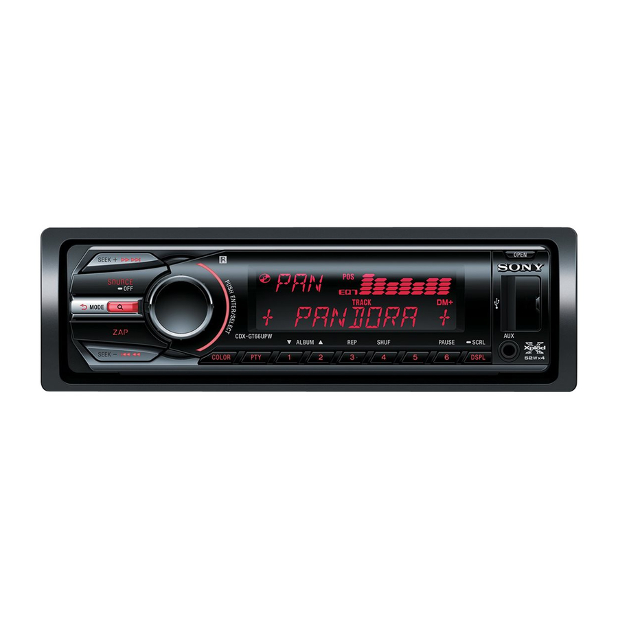
CDX-GT66UPW
Model Name Using Similar Mechanism
Mechanism Type
Optical Pick-up Name
SPECIFICATIONS
USB Player section
Interface: USB (Full-speed)
Maximum current: 1 A
Power amplifier section
Output: Speaker outputs
Speaker impedance: 4 – 8 ohms
Maximum power output: 52 W × 4 (at 4 ohms)
General
Outputs:
Audio outputs terminal (front/rear)
Subwoofer output terminal (mono)
Power antenna (aerial)/Power amplifier control
terminal (REM OUT)
Inputs:
Remote controller input terminal
Antenna (aerial) input terminal
Telephone ATT control terminal
AUX input jack (stereo mini jack)
USB signal input connector
Power requirements: 12 V DC car battery
(negative ground (earth))
Dimensions: Approx. 178 × 50 × 180 mm
1
1
(7
/
× 2 × 7
/
in) (w/h/d)
8
8
Mounting dimensions: Approx. 182 × 53 × 162 mm
1
1
1
(7
/
× 2
/
× 6
/
in) (w/h/d)
4
8
2
Mass: Approx. 1.3 kg (2 lb 14 oz)
Supplied accessories:
Remote commander: RM-X211
Parts for installation and connections (1 set)
Your dealer may not handle some of the above
listed accessories. Please ask the dealer for
detailed information.
Design and specifications are subject to change
without notice.
FM/AM COMPACT DISC PLAYER
US Model
CDX-GT660UP
MG-101CA-188
DAX-25A
System requirements for using
SensMe™
Computer
CPU/RAM
– IBM PC/AT compatible machine
– CPU: Intel Pentium III Processor 450 MHz
or higher
– RAM: 256 MB or more (For Windows XP),
512 MB or more (For Windows Vista or
later)
USB port
OS
Windows XP, Windows Vista, Windows 7
For details on compatible editions or Service
Pack, visit the support site on the back cover.
Monitor
High color (16-bit) or more, 800 × 600 dots or more
Other
Internet connection
Notes
The following system environments are not
supported.
– Non IBM PC type computers, such as
Macintosh, etc.
– Homemade computers
– OS upgraded computers
– Multi-display environment
– Multi-boot environment
– Virtual machine environment
Depending on the computer condition,
operation may not be possible even with the
recommended environment.
Advertisement
Table of Contents

Related Manuals for Sony CDX-GT66UPW


Summary of Contents for Sony CDX-GT66UPW
- Page 1 Design and specifications are subject to change Depending on the computer condition, without notice. operation may not be possible even with the recommended environment. FM/AM COMPACT DISC PLAYER 9-893-486-01 Sony Corporation 2012F33-1 © 2012.06 Published by Sony Techno Create Corporation...
- Page 2 (within 3 times). REPLACE THESE COMPONENTS WITH SONY PARTS • Be careful not to apply force on the conductor when soldering WHOSE PART NUMBERS APPEAR AS SHOWN IN THIS or unsoldering. MANUAL OR IN SUPPLEMENTS PUBLISHED BY SONY.
-
Page 3: Table Of Contents
CDX-GT66UPW SECTION 1 SERVICING NOTES TABLE OF CONTENTS NOTES ON HANDLING THE OPTICAL PICK-UP BLOCK OR BASE UNIT SERVICING NOTES ..........The laser diode in the optical pick-up block may suffer electro- GENERAL static break-down because of the potential difference generated by .............. - Page 4 CDX-GT66UPW EXTENSION CABLE AND SERVICE POSITION When repairing or servicing this set, connect the jig cable (exten- sion cable (CD mecha)) as shown below. • Connect the MAIN board (CN700) and the SERVO board (CN401) with the jig cable. Jig cable: Part No.
-
Page 5: General
CDX-GT66UPW SECTION 2 This section is extracted GENERAL from instruction manual. Equipment used in illustrations (not supplied) Equipo utilizado en las ilustraciones (no suministrado) FRONT AUDIO OUT Front speaker Subwoofer Power amplifier Rear speaker Altavoz frontal Altavoz potenciador de Amplificador de potencia... - Page 6 You may not be able to install this unit in some makes of Choose the installation location carefully so that the unit Japanese cars. In such a case, consult your Sony dealer. will not interfere with normal driving operations. Note...
-
Page 7: Disassembly
CDX-GT66UPW SECTION 3 DISASSEMBLY • This set can be disassembled in the order shown below. 3-1. DISASSEMBLY FLOW FRONT PANEL SECTION Note: Illustration of disassembly is omitted. 3-2. COVER (Page 7) 3-3. PANEL (SUB) BLOCK (Page 8) 3-4. CD MECHANISM DECK (MG-101CA-188) (Page 8) 3-5. -
Page 8: Panel (Sub) Block
CDX-GT66UPW 3-3. PANEL (SUB) BLOCK 2 two claws 3 Remove the panel (sub) block. 2 two claws 1 two screws 4 flexible flat cable (23 core) (PTT2.6 (CN102) 5 panel (sub) block 3-4. CD MECHANISM DECK (MG-101CA-188) 5 bracket (CD) -
Page 9: Main Board
CDX-GT66UPW 3-5. MAIN BOARD 3 screw (PTT2.6 1 fuse (blade type) (auto fuse) (10A/32V) (FU301) 2 three ground point screws (PTT2.6 3 screw (PTT2.6 4 MAIN board 3-6. SERVO BOARD 2 toothed lock screw (M1.7 2.5) 2 toothed lock screw (M1.7... -
Page 10: Chassis (T) Sub Assy
CDX-GT66UPW 3-7. CHASSIS (T) SUB ASSY 1 two screws (M1.7 2.5) 1 two screws (M1.7 2.5) 3 chassis (T) sub assy 2 claw 3-8. ROLLER ARM ASSY 5 roller arm assy 4 gear (HRA) 1 spring (RAL) 3 washer 2 spring (RAR) -
Page 11: Chassis (Op) Assy
CDX-GT66UPW 3-9. CHASSIS (OP) ASSY 8 chassis (OP) assy 1 tension spring (KF) 6 two coil springs (damper) (natural) 7 coil spring (damper) (blue) 4 slider (R) 3 lever (D) 2 gear (LE1) 3-10. CHUCKING ARM SUB ASSY 3 chucking arm sub assy 1 spring Note 1: Have this portion receive the chassis. -
Page 12: Sled Motor Assy
CDX-GT66UPW 3-11. SLED MOTOR ASSY 2 three serration screws 3 sled motor assy 1 spring turn table spring stand Note 2: Never remove these parts since they were adjusted. bearing (F) – – stand Note 1: Place the stand with care not to touch the turn table. -
Page 13: Optical Pick-Up Section
CDX-GT66UPW 3-12. OPTICAL PICK-UP SECTION 2 optical pick-up section Note: Be careful not to touch the lens and hologram terminal when removing the optical pick-up section. – bottom side view – 3-13. OPTICAL PICK-UP 1 tapping screw (P 1.4) 2 leaf spring (OPS) -
Page 14: Diagrams
CDX-GT66UPW SECTION 4 DIAGRAMS 4-1. BLOCK DIAGRAM - SERVO Section - CD MECHANISM DECK BLOCK (MG-101CA-188) FL, RL, SUB (Page 15) FPI1 DAO3 (F_L-CH) FPI2 DAO2 (F_R-CH) R-CH FNI1 FNI2 DAO4 (R_L-CH) DAO1 (R_R-CH) R-CH CD HEAD AMP, DAO5 (SUB-CH) -
Page 15: Block Diagram - Main Section
CDX-GT66UPW 4-2. BLOCK DIAGRAM - MAIN Section - ELECTRICAL VOLUME, INPUT SELECTOR IC401 J403 FL, RL, SUB (Page 14) 33 AU_IN_FL AU_OUT_FL 36 FRONT AUDIO OUT 31 AU_IN_RL R-CH AU_OUT_RL 38 REAR AUDIO OUT R-CH 30 AU_IN_SUB AU_OUT_SUB 39 J901... -
Page 16: Block Diagram - Panel, Power Supply Section
CDX-GT66UPW 4-3. BLOCK DIAGRAM - PANEL, POWER SUPPLY Section - SYSTEM CONTROLLER IC501 (3/3) (Page 14) RESET XOUT RESET X502 +3.3V SIGNAL 32.768kHz RESET 12 REGULATOR GENERATOR IC402 IC403 CN301 (2/2) OSCOUT X501 BU +3.3V REGULATOR LIQUID CRYSTAL DISPLAY PANEL LIQUID CRYSTAL DISPLAY DRIVER 7.92MHz... - Page 17 CDX-GT66UPW THIS NOTE IS COMMON FOR PRINTED WIRING BOARDS AND SCHEMATIC DIAGRAMS. • Circuit Boards Location (In addition to this, the necessary note is printed in each block.) For Printed Wiring Boards. For Schematic Diagrams. SERVO board Note: Note: SENSOR board •...
-
Page 18: Printed Wiring Board - Main Section (1/2)
CDX-GT66UPW 4-4. PRINTED WIRING BOARD - MAIN Section (1/2) - • See page 17 for Circuit Boards Location. • : Uses unleaded solder. X501, X701 MAIN BOARD (COMPONENT SIDE) R308 C457 C319 C397 Q403 Q405 Q404 Q401 Q402 D301 R303... -
Page 19: Printed Wiring Boards - Main Section (2/2)
CDX-GT66UPW 4-5. PRINTED WIRING BOARDS - MAIN Section (2/2) - • See page 17 for Circuit Boards Location. • : Uses unleaded solder. J403 REAR FRONT AUDIO OUT AUDIO OUT SUB OUT J801 FU301 MAIN BOARD (MONO) REMOTE IN (CONDUCTOR SIDE) -
Page 20: Schematic Diagram - Main Section (1/4)
CDX-GT66UPW 4-6. SCHEMATIC DIAGRAM - MAIN Section (1/4) - • See page 27 for IC Block Diagrams. MAIN BOARD (1/4) IC B/D IC301 POWER AMP, REGULATOR IC301 TDF8556AJ/N5 CN301 FRONT LCH (-) FRONT LCH (+) FRONT AUDIO OUT REAR LCH (-) -
Page 21: Schematic Diagram - Main Section (2/4)
CDX-GT66UPW 4-7. SCHEMATIC DIAGRAM - MAIN Section (2/4) - • See page 27 for Waveforms. • See page 27 for IC Block Diagrams. • See page 30 for IC Pin Function Description. MAIN BOARD (2/4) MAIN A_ATT BOARD (1/4) (Page 20) -
Page 22: Schematic Diagram - Main Section (3/4)
CDX-GT66UPW 4-8. SCHEMATIC DIAGRAM - MAIN Section (3/4) - • See page 27 for Waveforms. • See page 30 for IC Pin Function Description. MAIN BOARD (3/4) JL728 C771 R742 C787 C776 JL730 C717 C782 C779 C789 0.01 2200p FB782... -
Page 23: Schematic Diagram - Main Section (4/4)
CDX-GT66UPW 4-9. SCHEMATIC DIAGRAM - MAIN Section (4/4) - • See page 27 for Waveforms. • See page 27 for IC Block Diagrams. • See page 30 for IC Pin Function Description. MAIN BOARD (4/4) R674 R673 C616 R667 C613... -
Page 24: Printed Wiring Board - Sub Board
CDX-GT66UPW 4-10. PRINTED WIRING BOARD - SUB Board - 4-11. SCHEMATIC DIAGRAM - SUB Board - • See page 17 for Circuit Boards Location. • : Uses unleaded solder. SUB BOARD (Page 25) KEY BOARD CN901 FFC1 CN201 SUB BOARD... -
Page 25: Printed Wiring Board - Key Board
CDX-GT66UPW 4-12. PRINTED WIRING BOARD - KEY Board - • See page 17 for Circuit Boards Location. • : Uses unleaded solder. KEY BOARD (COMPONENT SIDE) S952 SEEK+ M > IC984 S951 SOURCE D978 C905 D977 LED988 R971 LCD901 6 5 4... -
Page 26: Schematic Diagram - Key Board
CDX-GT66UPW 4-13. SCHEMATIC DIAGRAM - KEY Board - • See page 27 for IC Block Diagrams. KEY BOARD LED988 LED989 SMLV56RGB1U1 SMLV56RGB1U1 (LCD BACKLIGHT) (KEY ILLUMINATION) R900 R983 R988 IC984 R910 R911 R912 R984 REMOTE CONTROL RECEIVER R985 IC984 LED990... - Page 27 CDX-GT66UPW • Waveforms • IC Block Diagrams – MAIN Board – – MAIN Board – IC301 TDF8556AJ/N5 IC501 qa (XOUT) I2C_SIO OUT-FL– C BUS I2C_SCK 2.6 Vp-p OUT-FL+ 30.4 s OUT-RL– 1 V/DIV, 20 s/DIV P-GND1 OUT-RL+ IC501 qd (OSCOUT)
- Page 28 CDX-GT66UPW IC681, 682 NJM2878F3-15 (TE2) THERMAL PROTECTION BANDGAP REFERENCE IC401 BD3467FV-E2 FADER FADER BOOST OUTC FADER FADER A1 1 BOOST OUTS A2 2 FADER FADER B1 3 OUTR1 BOOST B2 4 FADER FADER OUTR2 BOOST CP1 5 FADER FADER CN 6...
- Page 29 CDX-GT66UPW IC1300 OZ539IGN-A1-0-TR – KEY Board – IC971 74LVC2G66DC-125 BST 1 VREF OSCILLATOR LX 2 REFERENCE GENERATOR OVER CURRENT PROTECTION GNDA VIN 3 EN_SYS 4 USBOUT 5 FB_USB 6 SS_SYS ADJUSTMENT GENERATOR CHARGE EN_USB PUMP VIC_USB USBIN OVER-CURRENT ISET_USB LIMIT...
- Page 30 CDX-GT66UPW • IC Pin Function Description MAIN BOARD IC501 R5F3650KBDZ73FA (SYSTEM CONTROLLER) Pin No. Pin Name Description LCD_SO Serial data output to the liquid crystal display driver LCD_CLK Serial clock signal output to the liquid crystal display driver NOSE_SW Front panel remove/attach detection signal input terminal Fixed at “L”...
- Page 31 CDX-GT66UPW Pin No. Pin Name Description DIAG Diagnostic signal input from the power amplifi er AMPSTB Standby control signal output to the power amplifi er Not used VCC2 Power supply terminal (+3.3V) F_AUX_ATT Muting on/off control signal output terminal Ground terminal...
- Page 32 CDX-GT66UPW MAIN BOARD IC601 M321FEFG-7KN3 (SY (CD DRIVE/USB CONTROLLER) Pin No. Pin Name Description AVSS Ground terminal VREFH Reference voltage (+3.3V) input terminal (for A/D converter) RESET Reset signal input from the system controller “L”: reset MODE Operation mode setting terminal Fixed at “L”...
- Page 33 CDX-GT66UPW Pin No. Pin Name Description TRACEDATA0 to 64 to 67 Not used TRACEDATA3 CP_SDA Serial data input/output for the EEPROM CP_SCL Serial data transfer clock signal output to the EEPROM Not used CP_RESET Reset signal output to the EEPROM...
- Page 34 CDX-GT66UPW MAIN BOARD IC701 TC94A99FG-003 (SY, H (CD HEAD AMP, DIGITAL SERVO PROCESSOR, AUDIO DSP) Pin No. Pin Name Description LPFO Signal output from the operation amplifi er for PLL loop fi lter PVREF Reference voltage (+1.65V) input terminal VCOF Terminal for VCO fi...
- Page 35 CDX-GT66UPW Pin No. Pin Name Description ADVDD3 Power supply terminal (+3.1V) ADIN1 (IN_L-CH) Audio signal input terminal (L channel) ADVREFL Reference voltage output terminal ADVCM Reference voltage output terminal ADVREFH Reference voltage output terminal ADIN2 (IN_R-CH) Audio signal input terminal (R channel)
-
Page 36: Exploded Views
CDX-GT66UPW SECTION 5 EXPLODED VIEWS Note: • -XX and -X mean standardized parts, so • The mechanical parts with no reference The components identifi ed by mark 0 they may have some difference from the number in the exploded views are not sup- or dotted line with mark 0 are critical for original one. -
Page 37: Front Panel Section
CDX-GT66UPW 5-2. FRONT PANEL SECTION not supplied (for FRONT PANEL) not supplied (KEY board) RE901 not supplied supplied not supplied CCB1 LCD901 not supplied J901 CN971 CCB2 not supplied Note: Refer to the servicing notes “NOTE FOR REPLACEMENT OF THE USB CONNECTOR (CN971) AND THE AUX JACK (J901)”... -
Page 38: Cd Mechanism Deck Section (Mg-101Ca-188)
CDX-GT66UPW 5-3. CD MECHANISM DECK SECTION (MG-101CA-188) CDM1 DAX1 not supplied supplied not supplied not supplied not supplied not supplied not supplied SENSOR board not supplied not supplied not supplied not supplied not supplied Ref. No. Part No. Description Remark Ref. -
Page 39: Electrical Parts List
CDX-GT66UPW SECTION 6 ELECTRICAL PARTS LIST Note: • Due to standardization, replacements in • CAPACITORS The components identifi ed by mark 0 uF: μF the parts list may be different from the or dotted line with mark 0 are critical for parts specifi... - Page 40 CDX-GT66UPW MAIN Ref. No. Part No. Description Remark Ref. No. Part No. Description Remark R947 1-216-810-11 METAL CHIP 1/10W A-1885-299-A MAIN BOARD, COMPLETE R951 1-216-820-11 METAL CHIP 1/10W ******************** R952 1-216-821-11 METAL CHIP 1/10W R953 1-216-821-11 METAL CHIP 1/10W 7-685-134-19 SCREW +P 2.6X8 TYPE2 NON-SLIT...
- Page 41 CDX-GT66UPW MAIN Ref. No. Part No. Description Remark Ref. No. Part No. Description Remark C502 1-164-937-11 CERAMIC CHIP 0.001uF C735 1-114-582-91 CERAMIC CHIP 0.1uF C503 1-162-923-11 CERAMIC CHIP 47PF C737 1-100-742-91 CERAMIC CHIP 2.2uF C504 1-100-597-91 CERAMIC CHIP 0.1uF C738 1-100-742-91 CERAMIC CHIP 2.2uF...
- Page 42 CDX-GT66UPW MAIN Ref. No. Part No. Description Remark Ref. No. Part No. Description Remark D102 6-503-205-01 DIODE RKZ6.8B2KGP1 FB762 1-216-864-11 SHORT CHIP D103 6-503-205-01 DIODE RKZ6.8B2KGP1 FB782 1-469-084-21 FERRITE D104 6-503-205-01 DIODE RKZ6.8B2KGP1 FB801 1-500-113-22 BEAD, FERRITE (CHIP) (1608) D105 6-503-205-01 DIODE RKZ6.8B2KGP1...
- Page 43 CDX-GT66UPW MAIN Ref. No. Part No. Description Remark Ref. No. Part No. Description Remark R121 1-216-797-11 METAL CHIP 1/10W R500 1-218-957-11 METAL CHIP 2.2K 1/16W R122 1-216-797-11 METAL CHIP 1/10W R501 1-218-977-11 METAL CHIP 100K 1/16W R199 1-216-864-11 SHORT CHIP...
- Page 44 CDX-GT66UPW MAIN Ref. No. Part No. Description Remark Ref. No. Part No. Description Remark R577 1-218-977-11 METAL CHIP 100K 1/16W R684 1-218-965-11 METAL CHIP 1/16W R578 1-216-833-11 METAL CHIP 1/10W R686 1-218-969-11 METAL CHIP 1/16W R579 1-216-833-11 METAL CHIP 1/10W...
- Page 45 CDX-GT66UPW MAIN SENSOR SERVO Ref. No. Part No. Description Remark Ref. No. Part No. Description Remark R864 1-216-864-11 SHORT CHIP FFC1 1-834-627-11 CABLE, FLEXIBLE FLAT (23 CORE) R865 1-216-864-11 SHORT CHIP A-1885-300-A PANEL COMPLETE ASSY, FRONT R899 1-216-296-11 SHORT CHIP...
- Page 46 CDX-GT66UPW REVISION HISTORY Checking the version allows you to jump to the revised page. Also, clicking the version at the top of the revised page allows you to jump to the next revised page. Ver. Date Description of Revision 2012.06...