Sony CDX-GT690UI Service Manual
Fm/am compact disc player
Hide thumbs
Also See for CDX-GT690UI:
- Operating instructions manual (84 pages) ,
- Operating instructions manual (52 pages)
Table of Contents
Advertisement
Quick Links
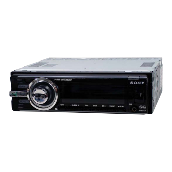
CDX-GT690UI/GT696UI
SERVICE MANUAL
Ver. 1.0 2009.10
• The tuner and CD sections have no adjustments.
Tuner section
FM
Tuning range:
Except Saudi Arabia model:
87.5 – 108.0 MHz (at 50 kHz step)
87.5 – 107.9 MHz (at 200 kHz step)
Saudi Arabia model:
87.5 – 108.0 MHz
FM tuning interval:
Except Saudi Arabia model:
50 kHz/200 kHz switchable
Antenna (aerial) terminal:
External antenna (aerial) connector
Intermediate frequency: 150 kHz
Usable sensitivity: 10 dBf
Selectivity: 75 dB at 400 kHz
Signal-to-noise ratio: 70 dB (mono)
Separation: 40 dB at 1 kHz
Frequency response: 20 – 15,000 Hz
Sony Corporation
9-889-673-01
2009J04-1
Audio&Video Business Group
©
2009.10
Published by Sony Techno Create Corporation
SPECIFICATIONS
AM
Tuning range:
Except Saudi Arabia model:
531 – 1,602 kHz (at 9 kHz step)
530 – 1,710 kHz (at 10 kHz step)
Saudi Arabia model:
531 – 1,602 kHz
AM tuning interval:
Except Saudi Arabia model:
9 kHz/10 kHz switchable
Antenna (aerial) terminal:
External antenna (aerial) connector
Intermediate frequency: 25 kHz
Sensitivity: 26 μV
CD Player section
Signal-to-noise ratio: 120 dB
Frequency response: 10 – 20,000 Hz
Wow and fl utter: Below measurable limit
FM/AM COMPACT DISC PLAYER
Model Name Using Similar Mechanism
CD Drive Mechanism Type
Optical Pick-up Name
USB Player section
Interface: USB (Full-speed)
Maximum current: 500mA
Power amplifi er section
Outputs: Speaker outputs (sure seal connectors)
Speaker impedance: 4 – 8 ohms
Maximum power output: 52 W × 4 (at 4 ohms)
E Model
CDX-GT690UI
Indian Model
CDX-GT696UI
CDX-GT680UI/
GT686UI
MG-101Z-188//Q
DAX-25A
– Continued on next page –
Advertisement
Table of Contents

Related Manuals for Sony CDX-GT690UI


Summary of Contents for Sony CDX-GT690UI
- Page 1 Separation: 40 dB at 1 kHz Frequency response: 10 – 20,000 Hz Frequency response: 20 – 15,000 Hz Wow and fl utter: Below measurable limit FM/AM COMPACT DISC PLAYER Sony Corporation 9-889-673-01 2009J04-1 Audio&Video Business Group © 2009.10 Published by Sony Techno Create Corporation...
- Page 2 COMPONENTS IDENTIFIED BY MARK 0 OR DOTTED LINE WITH MARK 0 ON THE SCHEMATIC DIAGRAMS AND IN THE PARTS LIST ARE CRITICAL TO SAFE OPERATION. REPLACE THESE COMPONENTS WITH SONY PARTS WHOSE PART NUMBERS APPEAR AS SHOWN IN THIS MANUAL OR IN SUPPLEMENTS PUBLISHED BY SONY.
-
Page 3: Table Of Contents
CDX-GT690UI/GT696UI This compact disc player is classifi ed as a CLASS 1 LASER TABLE OF CONTENTS product.The CLASS 1 LAZER PRODUCT label is located on the exterior. SERVICE NOTES ........... GENERAL Connections ..............DISASSEMBLY 3-1. Sub Panel Assy ............... This label is located on the bottom of the chassis. -
Page 4: Service Notes
CDX-GT690UI/GT696UI SECTION 1 SERVICE NOTES EXTENSION CABLE AND SERVICE POSITION When repairing or servicing this set, connect the jig (extension cable) as shown below. • Connect the MAIN board (CN201) and the SERVO board (CN401) with the extension cable (Part No. J-2502-076-1). -
Page 5: General
CDX-GT690UI/GT696UI SECTION 2 GENERAL This section is extracted from instruction manual. • CONNECTIONS RCA pin cord (not supplied) Supplied with the CD changer Separate adaptor may be required. FRONT REMOTE SUB OUT (MONO) AUDIO OUT Cable con terminales RCA (no... -
Page 6: Disassembly
CDX-GT690UI/GT696UI SECTION 3 DISASSEMBLY • This set can be disassembled in the order shown below. 3-1. SUB PANEL ASSY (Page 7) 3-2. CD MECHANISM BLOCK (Page 7) 3-4. SERVO BOARD 3-3. MAIN BOARD (Page 8) (Page 8) 3-5. CHASSIS (T) SUB ASSY (Page 9) 3-6. -
Page 7: Sub Panel Assy
CDX-GT690UI/GT696UI Note: Follow the disassembly procedure in the numerical order shown below. 3-1. SUB PANEL ASSY 3 two claws 4 CN203 (3P) 2 two claws 5 flexible flat cable (21 core) 1 two screws (CN902) (+PTT 2.6 6 sub panel assy 3-2. -
Page 8: Main Board
CDX-GT690UI/GT696UI 3-3. MAIN BOARD 7 screw 8 two screws 5 screw 2 two screws (+PTT 2.6 (+P 2.6 (+PTT 2.6 (+PTT 2.6 9 two screws (+PTT 2.6 0 two screws 1 three ground point screws (+P 2.6 (+PTT 2.6 6 connection cord qa screw (+PTT 2.6... -
Page 9: Chassis (T) Sub Assy
CDX-GT690UI/GT696UI 3-5. CHASSIS (T) SUB ASSY 2 two screws 1 two screws (M 1.7 2.5) (M 1.7 2.5) 4 chassis (T) sub assy 3 claw 3-6. ROLLER ARM ASSY 6 roller arm assy 4 gear (RA1) 1 spring (RAL) 3 washer... -
Page 10: Chassis (Op) Assy
CDX-GT690UI/GT696UI 3-7. CHASSIS (OP) ASSY 6 chassis (OP) assy 1 tension spring (KF) 7 two coil springs (damper) (natural) 8 coil spring (damper) (green) 4 slider (R) 3 lever (D) 2 gear (LE1) 3-8. CHUCKING ARM SUB ASSY 3 chucking arm sub assy 1 spring Note: Have this portion receive the chassis. -
Page 11: Sled Motor Assy
CDX-GT690UI/GT696UI 3-9. SLED MOTOR ASSY 2 three serration screws (M 2 3 sled motor assy 1 spring turn table spring stand Note: Never remove these parts since they were adjusted. bearing (F) stand Note: Place the stand with care not to touch the turn table. -
Page 12: Optical Pick-Up Section
CDX-GT690UI/GT696UI 3-10. OPTICAL PICK-UP SECTION 2 optical pick-up section Note: Be careful not to touch the lens and hologram terminal when removing the optical pick-up section. 3-11. OPTICAL PICK-UP 1 tapping screw (P 1.4) 2 leaf spring (OPS) 3 rack... -
Page 13: Diagrams
CDX-GT690UI/GT696UI SECTION 4 DIAGRAMS 4-1. BLOCK DIAGRAM – MAIN Section – ELECTRONIC VOLUME SUB OUT IC401 (MONO) J901 (1/2) 1 BUS_LCH OUT_SLCH R-CH AUDIO IN 2 BUS_RCH REAR R-CH J901 (2/2) R-CH AUDIO R-CH ZAP_BEEP J901 I2C BUS CONTROLLED FRONT... -
Page 14: Block Diagram -Display Section
CDX-GT690UI/GT696UI 4-2. BLOCK DIAGRAM – DISPLAY Section – SYSTEM CONTROL LCD DRIVER,LED CONTROL IC501 (2/2) IC981 KEY_IN1 KEY MATRIX LCD901 LCD_SO RING ILLUMI S201,951–966 LCD_SCK LIQUID PANEL+B LED DRIVER KEY_IN0 CRYSTAL LCD_CE Q992 DISPLAY 46 KEY_ACK1 PANEL LED991,992 LED901-916 LED921-936,... - Page 15 CDX-GT690UI/GT696UI THIS NOTE IS COMMON FOR PRINTED WIRING BOARDS AND SCHEMATIC DIAGRAMS. • Waveforms (In addition to this, the necessary note is printed in each block.) – MAIN Board – For Printed Wiring Boards: For Schematic Diagrams: Note: Note: IC1 qh (XTAL1) •...
-
Page 16: Printed Wiring Board -Main Section
CDX-GT690UI/GT696UI 4-3. PRINTED WIRING BOARD – MAIN Section – • : Uses unleaded solder. J901 AUDIO OUT AUDIO IN REAR FRONT J701 (REMOTE IN) J601 (BUS CONTROL IN) C305 C304 CN701 C302 C307 C306 R921 R922 JW100 IC301 C901 C902... -
Page 17: Schematic Diagram -Main Section (1/3)
CDX-GT690UI/GT696UI 4-4. SCHEMATIC DIAGRAM – MAIN Section (1/3) – • See page 24 for IC Block Diagrams. MAIN BOARD (1/3) IC301 IC B/D IC301 TDA8588AJ/N2/R1 I2C BUS CONTROLLED POWER AMP/MULTIPLE VOLTAGE REGULATOR CN701 FRONT L-CH – REAR L-CH – C308... -
Page 18: Schematic Diagram -Main Section (2/3)
CDX-GT690UI/GT696UI 4-5. SCHEMATIC DIAGRAM – MAIN Section (2/3) – • See page 15 for Waveforms. • See page 24 for IC Block Diagrams. MAIN BOARD (2/3) C912 CN901 100p SUB_OUT SUB OUT (MONO) IC B/D SUB_OUT PHASE LOCKED LOOP(PLL) IC B/D... -
Page 19: Schematic Diagram -Main Section (3/3)
CDX-GT690UI/GT696UI 4-6. SCHEMATIC DIAGRAM – MAIN Section (3/3) – • See page 15 for Waveforms. • See page 26 for IC Block Diagrams. • See page 27 for IC Pin Function Description of IC501. (Page 17) MAIN BOARD (1/3) MAIN BOARD... -
Page 20: Printed Wiring Board -Sub Section
CDX-GT690UI/GT696UI 4-7. PRINTED WIRING BOARD – SUB Section – • : Uses unleaded solder. (Page 22) KEY BOARD CN901 LED201 CN201 LED202 S201 LED202 LED201,S201 (DOOR INDICATOR) 1-877-079- (11) (Page 16) MAIN BOARD CN902 R201 CD MECHANISM R202 CN202 UNIT... -
Page 21: Schematic Diagram -Sub Section
CDX-GT690UI/GT696UI 4-8. SCHEMATIC DIAGRAM – SUB Section – SUB BOARD CN201 AUX-R AUX-R AUX-GND AUX-GND KEY1 KEY1 KEY0 KEY0 KEYGND LCD-DATA LCD-DATA LCD-CE CN203 LCD-CE MECHANISM GND-USB D+ (USB) UNIT VBUS-USB D- (USB) (MG-101Z) GND-LCDLED GND (USB) BOARD R203 R201... -
Page 22: Printed Wiring Boards -Key Section
CDX-GT690UI/GT696UI 4-9. PRINTED WIRING BOARDS – KEY Section – : Uses unleaded solder. • SEEK+/ M > S953 S954 LED925 LED923 LED905 LED903 LED921 LED901 IC982 S953 S951 D977 S951 Q993 Q992 B C E LED927 B C E LED907... -
Page 23: Schematic Diagram -Key Section
CDX-GT690UI/GT696UI 4-10. SCHEMATIC DIAGRAM – KEY Section – • See page 26 for IC Block Diagrams. KEY BOARD LED903,923 LED905,925 LED907,927 LED902,922 LED909,929 LED911,931 LED913,933 LED915,935 SEEK+/ SOURCE 2/ALBUM + 4/SHUF 6/PAUSE Q992 LED906,926 LED908,928 LED910,930 LED912,932 LED914,934 LED916,936 LED901,921... - Page 24 CDX-GT690UI/GT696UI • IC Block Diagrams IC301 TDA8588AJ/N2/R1 (MAIN Board (1/3)) IC601 BA8271F-E2 (MAIN Board (1/3)) IC302 TK11133CSCL-G (MAIN Board (1/3)) BUS ON BUS_ON SWITCH I2C_SIO OVERHEAT & OUT-FL– OVERCURRENT C BUS RESET PROTECTION I2C_SCK SWITCH BUS_IN CONTROL OUT-FL+ CLK_IN CIRCUIT...
- Page 25 CDX-GT690UI/GT696UI IC401 BD3447AFV-E2 (MAIN Board (2/3)) I2C BUS LOGIC, FADER FADER FADER FADER FADER EFFECT 180°/0° 7 BAND 3 BAND P-EQ (TONE CONTROL) SPECTRUM ANALYZER /LEVEL METER VOLUME/MUTE SPEANA LVL METER LVL METER SPEANA INPUT GAIN INPUT SELECTOR (3 SIGLE-END AND 3 STEREO IS O)
- Page 26 CDX-GT690UI/GT696UI IC801 TPS40200DRG4 (MAIN Board (3/3)) UVLO ISNS DRIVER LOGIC E/A AND SS REFERENCE SOFT-START OVERCURRENT 700mV COMP ENABLE E/A IC802 TPS2051BDRG4 (MAIN Board (3/3)) CHARGE PUMP CURRENT DRIVER LIMIT UVLO THERMAL SENSE IC803 TC7WH123FU(TE12R) (MAIN Board (3/3)) IC971 74LVC2G66DC-125 (KEY Board)
- Page 27 Ground ― Regulator reference capacitor connecting pin UNISI SONY-BUS data input UNISO SONY-BUS data output UNISCK SONY-BUS clock signal output Not used. (Open) I2C_SIO IIC serial data input/output I2C_SCK IIC serial clock signal output Not used. (Open) ACC_IN Accessory power supply detect signal input...
- Page 28 CDX-GT690UI/GT696UI Pin No. Pin Name Description WAKE_UP CD mechanism deck micon wake up signal output MC_RX MC-BUS communication and CD mechanism deck micon communication RX input MC_TX MC-BUS communication and CD mechanism deck micon communication TX output Flash programming serial clock signal output...
-
Page 29: Exploded Views
CDX-GT690UI/GT696UI SECTION 5 EXPLODED VIEWS Note: • -XX and -X mean standardized parts, so • The mechanical parts with no reference The components identifi ed by mark 0 they may have some difference from the number in the exploded views are not sup- or dotted line with mark 0 are critical for original one. -
Page 30: Front Panel Section
CDX-GT690UI/GT696UI 5-2. FRONT PANEL SECTION not supplied (KEY board) RE901 not supplied not supplied (JACK board) not supplied CN971 not supplied LCD901 not supplied not supplied Ref. No. Part No. Description Remark Ref. No. Part No. Description Remark A-1734-467-A PANEL OVERALL ASSY, FRONT (GT690UI:E) -
Page 31: Cd Mechanism Section (Mg-101Z-188//Q)
CDX-GT690UI/GT696UI 5-3. CD MECHANISM SECTION (MG-101Z-188//Q) not supplied not supplied not supplied not supplied not supplied not supplied not supplied not supplied not supplied not supplied not supplied not supplied Ref. No. Part No. Description Remark Ref. No. Part No. -
Page 32: Electrical Parts List
CDX-GT690UI/GT696UI SECTION 6 JACK ELECTRICAL PARTS LIST Note: • Due to standardization, replacements in • RESISTORS The components identifi ed by mark 0 the parts list may be different from the All resistors are in ohms. or dotted line with mark 0 are critical for parts specifi... - Page 33 CDX-GT690UI/GT696UI Ref. No. Part No. Description Remark Ref. No. Part No. Description Remark LED916 6-502-542-01 LED SCM015BC7TT86P (DSPL/SCRL) R925 1-216-029-00 METAL CHIP 1/10W LED917 6-502-542-01 LED SCM015BC7TT86P (RING ILLUMINATOR) R926 1-216-295-91 SHORT CHIP LED918 6-502-542-01 LED SCM015BC7TT86P (RING ILLUMINATOR) R929...
- Page 34 CDX-GT690UI/GT696UI MAIN Ref. No. Part No. Description Remark Ref. No. Part No. Description Remark < ROTARY ENCODER > C207 1-164-739-11 CERAMIC CHIP 560PF C208 1-124-584-00 ELECT 100uF RE901 1-487-023-11 ENCODER, ROTARY C209 1-162-970-11 CERAMIC CHIP 0.01uF (PUSH ENTER/SELECT (VOLUME)) C301 1-115-340-11 CERAMIC CHIP 0.22uF...
- Page 35 CDX-GT690UI/GT696UI MAIN Ref. No. Part No. Description Remark Ref. No. Part No. Description Remark C513 1-162-964-11 CERAMIC CHIP 0.001uF < DIODE > C514 1-162-970-11 CERAMIC CHIP 0.01uF C601 1-165-319-11 CERAMIC CHIP 0.1uF D201 6-501-013-01 DIODE BAT54ALT1G C602 1-126-941-11 ELECT 470uF...
- Page 36 CDX-GT690UI/GT696UI MAIN Ref. No. Part No. Description Remark Ref. No. Part No. Description Remark IC803 8-759-586-19 IC TC7WH123FU(TE12R) < COIL > < JACK > 1-414-180-51 INDUCTOR 3.3uH 1-410-501-61 INDUCTOR 2.2uH 1-822-949-11 JACK (ANTENNA) 1-457-817-11 COIL (FM MIX) J601 1-580-907-41 PLUG, CONNECTOR 11P (BUS CONTROL IN)
- Page 37 CDX-GT690UI/GT696UI MAIN Ref. No. Part No. Description Remark Ref. No. Part No. Description Remark R111 1-216-864-11 SHORT CHIP R536 1-216-845-11 METAL CHIP 100K 1/10W R201 1-216-845-11 METAL CHIP 100K 1/10W R537 1-216-809-11 METAL CHIP 1/10W R202 1-216-864-11 SHORT CHIP R538...
- Page 38 CDX-GT690UI/GT696UI MAIN SERVO Ref. No. Part No. Description Remark Ref. No. Part No. Description Remark R814 1-216-842-11 METAL CHIP 1/10W SUB BOARD R815 1-216-833-11 METAL CHIP 1/10W ********** R816 1-216-821-11 METAL CHIP 1/10W R818 1-216-833-11 METAL CHIP 1/10W 1-835-781-11 CABLE, FLEXIBLE FLAT (21 CORE) (CN202)
- Page 39 CDX-GT690UI/GT696UI Ref. No. Part No. Description Remark PARTS FOR INSTALLATION AND CONNECTIONS ************************************** X-2179-431-2 FRAME ASSY, FITTING 1-833-972-11 CONNECTION CORD FOR AUTOMOBILE (POWER) 3-876-675-01 KEY (FRAME) X-3381-154-1 SCREW ASSY (BS4), FITTING 3-349-410-11 BUSHING 3-934-325-01 SCREW, +K (5X8) TAPPING 3-874-329-01 COLLAR...
- Page 40 CDX-GT690UI/GT696UI REVISION HISTORY Checking the version allows you to jump to the revised page. Also, clicking the version at the top of the revised page allows you to jump to the next revised page. Ver. Date Description of Revision 2009.10...