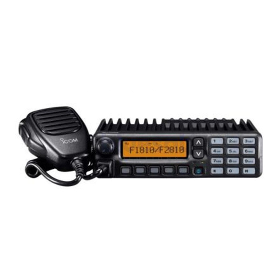
Icom IC-F1721/D Service Manual
Vhf mobile transceivers
Hide thumbs
Also See for IC-F1721/D:
- Operating manual (12 pages) ,
- Instruction manual (36 pages) ,
- Instruction manual (36 pages)
Table of Contents
Advertisement
Quick Links
Advertisement
Table of Contents

Related Manuals for Icom IC-F1721/D


Summary of Contents for Icom IC-F1721/D
- Page 1 SERVICE MANUAL VHF MOBILE TRANSCEIVERS iC-f1721/d iC-f1710 iC-f1821/d iC-f1810...
- Page 2 8. READ the instructions of test equipment thoroughly before connecting equipment to the transceiver. Icom, Icom Inc. and are registered trademarks of Icom Incorporated (Japan) in the United States, the United Kingdom, Germany, France, Spain, Russia and/or other countries.
-
Page 3: Table Of Contents
TABLE OF CONTENTS SECTION SPECIFICATIONS SECTION INSIDE VIEWS SECTION DISASSEMBLY INSTRUCTIONS SECTION CIRCUIT DESCRIPTION RECEIVER CIRCUITS ..........TRANSMITTER CIRCUITS . -
Page 4: Specifications
SECTION 1 SPECIFICATIONS ■ GENERAL • Frequency coverage : 136.000–174.000 MHz • Type of emission VERSION WIDE MIDDLE NARROW [USA] 11K0F3E (12.5 kHz) [GEN] 16K0F3E (25.0 kHz) 8K50F3E (12.5 kHz) [EUR] 14K0F3E (20.0 kHz) • Number of conventional channels : max 256 channels : 50 Ω... -
Page 5: Inside Views
SECTION 2 INSIDE VIEWS • MAIN UNIT Top view Power amplifier IC29: S-AV32 for IC-F1721/D, F1821/D S-AV33 for IC-F1710, F1810 APC circuit AF amplifier (IC37: TA75S01F) (IC38: LA4425A) Mixer circuit +5V regulator (Q31: 2SB1132) PLL IC D/A converter (IC4: LMX2352TM) - Page 6 • FRONT-A UNIT (IC-F1700 series) Reset IC LCD driver Mic amplifier (IC2: S-80942CNMC) (IC7: SED1526F0A) (IC5: TC75S51F) Backlight ALC amplifier Mic switch Front CPU dimmer control (IC9: AN6123MS) (IC8: TC4W53F) (IC3: HD64F3687) Q3: 2SC4116 Q4: DTC114TU Q5: DTC114TU • FRONT-B UNIT (IC-F1800 series) Reset IC LCD driver Mic amplifier...
-
Page 7: Section 3 Disassembly Instructions
SECTION 3 DISASSEMBLY INSTRUCTIONS • REMOVING THE FRONT UNIT 2 Unscrew 4 screws, G and remove the shield cover H. 1 Unscrew 4 screws, A, then remove the bottom cover. 3 Unsolder 3 points, I and 5 points J. w Unplug J1(B) and J6 (C). 4 Remove 2 clips, K. -
Page 8: Section 4 Circuit Description
SECTION 4 CIRCUIT DESCRIPTION 4-1 RECEIVER CIRCUITS 4-1-3 1ST MIXER AND 1ST IF CIRCUITS (MAIN UNIT) The 1st mixer circuit converts the received signals into 4-1-1 ANTENNA SWITCHING CIRCUIT (MAIN UNIT) fixed frequency of the 1st IF signal with the PLL output fre- The antenna switching circuit functions as a low-pass filter quency. - Page 9 The power amplified AF signals are applied to the internal A 2nd LO signal (45.9 MHz) is produced at the PLL circuit speaker (IC-F1700 series only) that is connected to J6 via by tripling it’s reference frequency (15.3 MHz). [EXT SP] jack (J5). The 2nd IF signal from the 2nd mixer section (IC12, pin 3) passes through the ceramic filter (Wide: FI1, Narrow: FI1, 4-1-6 SQUELCH CIRCUITS (MAIN UNIT)
-
Page 10: Transmitter Circuits
(D19), and is amplified at the YGR (Q23), power (IC29) (FRONT UNIT; J2, pin 6) are passed through the micro- amplifiers to obtain 50 W (IC-F1721/D/F1821/D; 25 W for phone switch (FRONT UNIT; IC8, pins 1, 6, 7) and are then IC-F1710/F1810) of RF power. -
Page 11: Pll Circuits
4-3 PLL CIRCUITS 4-4 POWER SUPPLY CIRCUITS 4-3-1 PLL CIRCUIT (MAIN UNIT) Line Description A PLL circuit provides stable oscillation of the transmit fre- The voltage from a DC power supply. quency and receive 1st LO frequency. The PLL output com- pares the phase of the divided VCO frequency to the refer- The same voltage as the HV line which is ence frequency. -
Page 12: Other Circuits
4-5 OTHER CIRCUITS 4-5-2 DIGITAL MODE CIRCUIT (IC-F1721D/F1821D only) (1) IN CASE OF RECEIVING 4-5-1 COMPANDER CIRCUIT (MAIN UNIT) Output signal from the FM IF IC (IC12, pin 11) is applied to IC-F1700/F1800 series have compander circuit which can the IF amplifi er (Q3), and is then amplifi ed at the IF amplifi er improve S/N ratio and become wide dynamic range. -
Page 13: Port Allocations
4-6 PORT ALLOCATIONS 4-6-1 MAIN CPU (MAIN UNIT; IC23) Port Port Description Description number name number name BEEP Outputs beep audio signals. I/O port for data signal to the D/A con- DSDA verter (IC30 pin 6). Input por t for single tone decode SDEC signal from the base band IC (IC2, Outputs strobe signals to the D/A... - Page 14 4-6-2 FRONT CPU (FRONT UNIT; IC3) 4-6-4 D/A CONVERTER (MAIN UNIT; IC30) Port Port Description Description number name number name Input port for rest signal. Outputs the bandpass filters (D23, D26) tuning signal. KR0– I n p u t p o r t s fo r t h e 1 0 - k e y p a d . 19–22 (IC-F1800 series only) •...
-
Page 15: Section 5 Adjustment Procedures
SECTION 5 ADJUSTMENT PROCEDURES 5-1 PREPARATION When adjusting IC-F1721/D,F1710,F1821/D,F1810, the optional CS-F1700 ADJ ADJUSTMENT SOFTWARE (Rev. 1.0 or later), OPC-1122* (modifi ed OPC-1122 ; see illustration page 5-3) are required. JIG CABLE CLONING CABLE ▄ REQUIRED TEST EQUIPMENT EQUIPMENT GRADE AND RANGE... - Page 16 • CS-F1700 ADJ'S SCREEN EXAMPLE NOTE: The above values for settings are example only. Each transceiver has its own specific values for each setting. !3 : PLL lock voltage for RX (automatic) q: Transceiver's connection state !4 : PLL lock voltage for TX (automatic) w: Reload adjustment data !5 : PLL lock voltage for RX (manual) e: Receive sensitivity measurement...
- Page 17 RS-232C port RS-232C cable (straight) to the MIC connector AC millivoltmeter IC-F1721/D/F1710 *OPC-1122 IC-F1821/D/F1810 (JIG CABLE) Audio generator • JIG CABLE • OPC-1122* (JIG CABLE) Add a jumper wire here PTT switch...
-
Page 18: Lcd Contrast Adjustment
5-2 SOFT WARE ADJUSTMENT Select an operation using [↑] / [↓] keys, then set specifi ed value using [←] / [→] keys on the connected computer keyboard MEASUREMENT ADJUSTMENT ADJUSTMENT CONDITION VALUE UNIT LOCATION UNIT ADJUST 1 • Operating freq. : 155.000 MHz FRON Connecta digital –2.0 V... - Page 19 5-3 SOFT WARE ADJUSTMENT Select an operation using [↑] / [↓] keys, then set specifi ed value using [←] / [→] keys on the connected computer keyboard MEASUREMENT ADJUSTMENT ADJUSTMENT CONDITION VALUE UNIT LOCATION PLL LOCK 1 • Operating CH. : CH 1 Check the "LVIN"...
- Page 20 SOFTWARE ADJUSTMENT (Continued) Select an operation using [↑] / [↓] keys, then set specifi ed value using [←] / [→] keys on the connected computer keyboard MEASUREMENT ADJUSTMENT ADJUSTMENT CONDITION VALUE UNIT LOCATION OUTPUT 1 • Operating CH. : CH 3 Rear Connect an RF power meter to 25.0 W [25W]...
- Page 21 SOFTWARE ADJUSTMENT (Continued) Select an operation using [↑] / [↓] keys, then set specifi ed value using [←] / [→] keys on the connected computer keyboard MEASUREMENT ADJUSTMENT ADJUSTMENT CONDITION VALUE UNIT LOCATION ±2.85 kHz 1 • Operating CH. : CH 6 DIGITAL Rear Connect a modulation ana-...
- Page 22 SOFTWARE ADJUSTMENT (continued) • Select an operation using [↑] / [↓]keys, then set specifi ed value using [←] / [→] keys on the connected computer keyboard • Need to adjust "S-METER ADJUSTMENT" after "RX SENSITIVITY ADJUSTMENT" is adjusted. Otherwise , "S-METER ADJUSTMENT" will not be adjusted properly. MEASUREMENT ADJUSTMENT ADJUSTMENT CONDITION...
-
Page 23: Section 6 Parts List
SECTION 6 PARTS LIST [FRONT-A UNIT] (for IC-F1700 series) [FRONT-A UNIT] (IC-F1700 series) ORDER ORDER DESCRIPTION DESCRIPTION LOCATION LOCATION 7030004980 S.RES ERJ2GEJ 101 X (100 Ω) 21.3/8.6 1110005770 S.IC S-80942CNMC-G9C-T2 81.9/29.8 7030005160 S.RES ERJ2GEJ 105 X (1 MΩ) 26.8/4.7 1140010770 S.IC HD64F3687FP 73.5/21.4 7030005220 S.RES ERJ2GEJ 223 X (22 kΩ) - Page 24 [FRONT-B UNIT] (for IC-F1800 series) [FRONT-A UNIT] (for IC-F1700 series) ORDER ORDER DESCRIPTION DESCRIPTION LOCATION LOCATION 7030005050 S.RES ERJ2GEJ 103 X (10 kΩ) 28.5/17.3 5040002310 S.LED SML-311YTT86 20.9/6.5 7030005120 S.RES ERJ2GEJ 102 X (1 kΩ) 17.6/15.9 5040002310 S.LED SML-311YTT86 93.4/6.5 7030005120 S.RES ERJ2GEJ 102 X (1 kΩ) 10.7/20.1 5040002310 S.LED SML-311YTT86...
- Page 25 [MAIN UNIT] [FRONT-B UNIT] (for IC-F1800 series) ORDER ORDER DESCRIPTION DESCRIPTION LOCATION LOCATION 4030017490 S.CER C1608 JB 1A 105K-T 54.3/25.7 1110005340 S.IC NJM12902V-TE1 75.1/36.2 1110006220 S.IC AK2346-E2 48.4/27.8 4030017490 S.CER C1608 JB 1A 105K-T 54.3/24.2 4030017460 S.CER ECJ0EB1E102K 53.4/21.1 1130010100 S.IC LMX2352TMX 75.6/56.2 4030017460 S.CER ECJ0EB1E102K...
- Page 26 [MAIN UNIT] [MAIN UNIT] ORDER ORDER DESCRIPTION DESCRIPTION LOCATION LOCATION 6050012130 S.XTL CR-802 (12.288 MHz) 1530002850 S.TR 2SC4116-BL (TE85R) [F1721D], [F1821D] only B 90.4/27.3 [F1721/D], [F1821/D] only T 46.2/80.6 1590000430 S.TR DTC144EUA T106 148/30.4 1590000430 S.TR DTC144EUA T106 146.4/36.8 6200004660 S.COL MLF1608A 1R8K-T 76.4/63.3 1590000430 S.TR DTC144EUA T106...
- Page 27 [MAIN UNIT] [MAIN UNIT] ORDER ORDER DESCRIPTION DESCRIPTION LOCATION LOCATION 7030005220 S.RES ERJ2GEJ 223 X (22 kΩ) 67.4/35.5 R126 7030005240 S.RES ERJ2GEJ 473 X (47 kΩ) 72.4/42.9 7030005220 S.RES ERJ2GEJ 223 X (22 kΩ) 69.2/35.5 R127 7030007290 S.RES ERJ2GEJ 222 X (2.2 kΩ) 71.2/45.7 7030005160 S.RES ERJ2GEJ 105 X (1 MΩ) 49.2/22.7...
- Page 28 [MAIN UNIT] [MAIN UNIT] ORDER ORDER DESCRIPTION DESCRIPTION LOCATION LOCATION 7030004980 S.RES ERJ2GEJ 101 X (100 Ω) R273 R202 7030005240 S.RES ERJ2GEJ 473 X (47 kΩ) [F1721D], [F1821D] only B 125.7/7.7 [F1721D], [F1821D] only B 90/32.8 R276 7030010040 S.RES ERJ2GE-JPW 75.4/99.5 R203 7030005240 S.RES ERJ2GEJ 473 X (47 kΩ)
- Page 29 [MAIN UNIT] [MAIN UNIT] ORDER ORDER DESCRIPTION DESCRIPTION LOCATION LOCATION 7030000020 S.RES MCR10EZHJ 1 Ω (010) R367 151.5/57.9 4030016970 S.CER ECJ0EB1C223K 52.8/23.2 7030000020 S.RES MCR10EZHJ 1 Ω (010) R368 151.5/47.4 4030017420 S.CER ECJ0EC1H470J 46.8/33.4 R370 7410000750 S.ARY EXB-V4V 104JV (100 kΩ) 96.9/76.1 4030016930 S.CER ECJ0EB1A104K 50.5/16...
- Page 30 [MAIN UNIT] [MAIN UNIT] ORDER ORDER DESCRIPTION DESCRIPTION LOCATION LOCATION C209 4030017420 S.CER ECJ0EC1H470J C121 4030016930 S.CER ECJ0EB1A104K 72.4/44.9 [F1721D], [F1821D] only B 92.8/6.5 C122 4030017730 S.CER ECJ0EB1E471K 70.9/41.4 C210 4030017460 S.CER ECJ0EB1E102K C123 4030017600 S.CER ECJ0EC1H080C 69.3/57.4 [F1721D], [F1821D] only B 91.1/22.2 C124 4550003220 S.TAN TEESVA 1E 105M8L...
- Page 31 [MAIN UNIT] [MAIN UNIT] ORDER ORDER DESCRIPTION DESCRIPTION LOCATION LOCATION C286 4030017460 S.CER ECJ0EB1E102K 60.6/61.8 C366 4510004630 S.ELE ECEV1CA100SR 101/58 C367 4030016930 S.CER ECJ0EB1A104K C287 4030017620 S.CER ECJ0EC1H100C 56.5/66 C288 4030017460 S.CER ECJ0EB1E102K 58.5/64.5 [F1721D], [F1821D] only T 107.7/12.5 C289 4030017340 S.CER ECJ0EC1H010B 61.3/69.5 C368...
- Page 32 [CHASSIS UNIT] [MAIN UNIT] ORDER ORDER DESCRIPTION DESCRIPTION LOCATION LOCATION 6510004880 CNR MR-DS-E 01 C464 4030017460 S.CER ECJ0EB1E102K T 150.4/107.8 C465 4030017460 S.CER ECJ0EB1E102K T 150.4/106.8 C467 4030017420 S.CER ECJ0EC1H470J T 150.4/104.8 C468 4510006240 S.ELE ECEV1CA221P 137.6/53.1 C469 4030017460 S.CER ECJ0EB1E102K 141/59.5 C470 4510006240 S.ELE ECEV1CA221P...
-
Page 33: Section 7 Mechanical Parts And Disassembly
SECTION 7 MECHANICAL PARTS AND DISASSEMBLY [CHASSIS PARTS] [MAIN UNIT] REF. NO. ORDER NO. QTY. DESCRIPTION REF. NO. ORDER NO. QTY. DESCRIPTION 6510004880 Connector MR-DS-E 01 8900013680 Cable OPC-1414 <CMI>T 8010019800 2781 chassis 6510023210 CD6125SA1J0 8110008270 2781 cover 8810008660 Screw PH BT M3 × 8 NI-ZU EP 9 6910010280 Bead HF70BB9.5X10.4X4.9 8810008660 Screw PH BT M3 ×... - Page 34 176 (6 MP6 (C) MP8 (C) J11 (M) MP1 (C) J11 (M) MP4 (C) MP12 (C) J1 (C) MP12 (F) FRONT-B UNIT Unit: mm (inch) MP22 (F) MP2 (F) 175 (6 W1 (F) MP5 (F) MP12 (F) EP1 (F) MP12 (C) EP1 (F) DS1 (F) MP3 (F)
-
Page 35: Section 8 Semi-Conductor Information
SECTION 8 SEMI-CONDUCTOR INFORMATION • • TRANSISTOR AND FET’S DIODES 1SS355 1SS375-TL 1SV239 DA204U DA221 TL 2SA1577 T106 Q 2SB1132 Q 2SC3356 T1B R25 2SC4116 BL 2SC4215 O (Symbol: A) (Symbol: FH) (Symbol: TC) (Symbol: K) (Symbol: K) (Symbol: HQ) (Symbol: BAQ) (Symbol: R25) (Symbol: LL) -
Page 36: Section 9 Board Layouts
SECTION 9 BOARD LAYOUTS The combination of this page and the next page shows the unit layout in the same configuration as the actual 9-1 FRONT-A UNIT (for IC-F1700 series) P.C. Board. • TOP VIEW DIAL AF VOLUME H100 H105 H110 H115 to MIC JACK... - Page 37 FRONT-A UNIT • BOTTOM VIEW (for IC-F1700 series) The combination of this page and the previous page shows the unit layout in the same configuration as the actual P.C. Board. H115 H110 H105 H100 to MAIN UNIT 9 - 2...
-
Page 38: Front-B Unit (For Ic-F1800 Series)
9-2 FRONT-B UNIT (for IC-F1800 series) • TOP VIEW The combination of this page and the next page shows the unit layout in the same configuration as the actual P.C. Board. AF VOLUME H100 H105 H110 H115 H120 H125 H130 H135 H140 H145... - Page 39 FRONT-B UNIT • BOTTOM VIEW (for IC-F1800 series) The combination of this page and the previous page shows the unit layout in the same configuration as the actual P.C. Board. H165 H160 H155 H150 H145 H140 H135 H130 H125 H120 H115 H110 H105...
- Page 40 The combination of this page and the next page shows the unit layout in the same configuration as the actual P.C. Board. 9-3 MAIN UNIT DC Cable to ANT • TOP VIEW V115 V110 IC29 Power amplifier V105 V100 to GPS Internal Speaker (IC-F1700 Series Only) –...
-
Page 41: Main Unit
EXT. The combination of this page and the previous page 25PIN Connector SPEAKER shows the unit layout in the same configuration as the MAIN UNIT actual P.C. Board. • BOTTOM VIEW V115 SP– V110 V105 V100 H160 H155 H150 H145 H140 H135 H130... -
Page 42: Block Diagram
LVIN HVC375B BUFF D6, D7: HVC376B x 2 Q11: 2SC4226 RLVA RXVCO IC29 D31: UM901F D38, D40 D19, D20 S-AV32: IC-F1721/D, F1821/D NJM12902V LMX2352TM MA77 ×2 1SS375 x 2 CR-794 2SC5107 2SC5107 2SC3356 D27: MA77 S-AV33: IC-F1710, F1810 15.3 MHz... -
Page 43: Voltage Diagram
SECTION 11 VOLTAGE DIAGRAM 11-1 FRONT-A UNIT (for IC-F1700 series) DIM OFF: 7.0 V ON : 6.2 V DS11 DS14 SML-311YT SML-311YT SML-311YT SML-311YT DS12 DS15 SML-311YT SML-311YT SML-311YT SML-311YT DS26 DS13 DS16 SML-311YT SML-311YT SML-311YT SML-311YT DS18 DTC114TU L4-0013TVY SML-512UW DTC114TU Light ON: 4.9 V... -
Page 44: Front-B Unit (For Ic-F1800 Series)
11-2 FRONT-B UNIT (for IC-F1800 series) DIM OFF: 7.0 V ON : 6.1 V DS24 DS22 DS19 DS11 DS14 SML-311YT SML-311YT SML-311YT SML-311YT SML-311YT SML-311YT SML-311YT DS25 DS23 DS20 DS12 DS15 SML-311YT SML-311YT SML-311YT SML-311YT SML-311YT SML-311YT SML-311YT DS26 DS10 DS21 DS13 DS16... -
Page 45: Main Unit
11-3 MAIN UNIT NJM12902V R22 330k 15.3 MHz CR-794 R3 100k 120k TONE R2 270k 950 mVp-p 15.3 MHz NJM12902V R4 68k MICA R1 10k VCON R8 220k C12 0.1 C135 R106 AFOUT DTC144EU TEMP TEMP C535 120k 180p 470p LVIN 0.001 CP37... - Page 46 R237 RX VCO 6.7 V C347 C284 C285 C120 R125 6.9 V R209 C281 R174 R127 R147 C220 C241 390p 0.001 C242 C257 0.01 R242 0.001 100k C153 C155 2.2k 3.9k 1.8k 0.01 470p R193 6.3 V 0.001 220p 0.01 2SC4116 C279 C156...
- Page 47 E-mail : info@icomcanada.com Unit 9, Sea St., Herne Bay, Kent, CT6 8LD, U.K. Phone : +44 (01227) 741741 Fax : +44 (01227) 741742 Icom (Australia) Pty. Ltd. : http://www.icomuk.co.uk E-mail : info@icomuk.co.uk A.B.N. 88 006 092 575 290-294 Albert Street, Brunswick, Victoria, 3056, Australia Icom France S.a...
- Page 48 S-14118MZ-C1 1-1-32, Kamiminami, Hirano-ku, Osaka 547-0003, Japan © 2004 Icom Inc.