
Related Manuals for Asus AAEON PICO-EHL4-A11


Summary of Contents for Asus AAEON PICO-EHL4-A11
- Page 1 PICO-EHL4-A11 PICO-ITX Single Board Computer User’s Manual 1 Last Updated: August 1, 2022...
- Page 2 Copyright Notice This document is copyrighted, 2022. All rights are reserved. The original manufacturer reserves the right to make improvements to the products described in this manual at any time without notice. No part of this manual may be reproduced, copied, translated, or transmitted in any form or by any means without the prior written permission of the original manufacturer.
- Page 3 Acknowledgement All other products’ name or trademarks are properties of their respective owners. Microsoft Windows® is a registered trademark of Microsoft Corp. ⚫ Intel®, Celeron® and Pentium® are registered trademarks of Intel Corporation ⚫ Intel Atom™ is a trademark of Intel Corporation ⚫...
- Page 4 Packing List Before setting up your product, please make sure the following items have been shipped: Item Quantity PICO-EHL4-A11 ⚫ If any of these items are missing or damaged, please contact your distributor or sales representative immediately. Preface...
- Page 5 About this Document This User’s Manual contains all the essential information, such as detailed descriptions and explanations on the product’s hardware and software features (if any), its specifications, dimensions, jumper/connector settings/definitions, and driver installation instructions (if any), to facilitate users in setting up their product. Users may refer to the product page on AAEON.com for the latest version of this document.
- Page 6 Safety Precautions Please read the following safety instructions carefully. It is advised that you keep this manual for future references All cautions and warnings on the device should be noted. Make sure the power source matches the power rating of the device. Position the power cord so that people cannot step on it.
- Page 7 If any of the following situations arises, please the contact our service personnel: Damaged power cord or plug Liquid intrusion to the device iii. Exposure to moisture Device is not working as expected or in a manner as described in this manual The device is dropped or damaged Any obvious signs of damage displayed on the device...
- Page 8 FCC Statement This device complies with Part 15 FCC Rules. Operation is subject to the following two conditions: (1) this device may not cause harmful interference, and (2) this device must accept any interference received including interference that may cause undesired operation.
- Page 9 China RoHS Requirements (CN) 产品中有毒有害物质或元素名称及含量 AAEON Main Board/ Daughter Board/ Backplane 有毒有害物质或元素 部件名称 铅 汞 镉 六价铬 多溴联苯 多溴二苯醚 (Pb) (Hg) (Cd) (Cr(VI)) (PBB) (PBDE) 印刷电路板 ○ ○ ○ ○ ○ ○ 及其电子组件 外部信号 ○ ○ ○ ○ ○ ○ 连接器及线材...
- Page 10 China RoHS Requirement (EN) Poisonous or Hazardous Substances or Elements in Products AAEON Main Board/ Daughter Board/ Backplane Poisonous or Hazardous Substances or Elements Hexavalent Polybrominated Polybrominated Component Lead Mercury Cadmium Chromium Biphenyls Diphenyl Ethers (Pb) (Hg) (Cd) (Cr(VI)) (PBB) (PBDE) PCB &...
-
Page 11: Table Of Contents
Table of Contents Chapter 1 - Product Specifications..................1 Specifications ......................2 Function Block Diagram ..................5 Chapter 2 – Hardware Information ..................6 Dimensions ....................... 7 Jumpers and Connectors ..................9 List of Jumpers ......................11 2.3.1 Clear CMOS Jumper & Auto Power Button Enable/Disable (JP1) 11 List of Connectors .................... - Page 12 2.4.18 Power Input +12V (CN20) ..............34 2.4.19 Front Panel (CN21) ................35 2.4.20 DC Jack Power Input [Reserved] (CN22) .......... 36 2.4.21 Single RJ45 [Reserved] (CN23) ............37 Thermal Assembly Options ................. 38 2.5.1 Active Cooling Fan FAN01 ..............38 2.5.2 Fan-less Heatspreader HSP01 .............
- Page 13 3.5.1.1 Memory Configuration ............63 3.5.1.2 Graphics Configuration ............64 3.5.2 PCH-IO Configuration ................67 Setup Submenu: Security ..................68 3.6.1 Secure Boot .................... 69 3.6.1.1 Key Management ..............70 Setup Submenu: Boot ..................72 Setup Submenu: Save & Exit ................73 Chapter 4 –...
- Page 14 C.3.1.6 EapiWDogGetStatus() ............104 C.3.1.7 EapiWDogSetStatus() ............105 Preface...
-
Page 15: Chapter 1 - Product Specifications
Chapter 1 Chapter 1 - Product Specifications... -
Page 16: Specifications
Specifications System Form Factor PICO-ITX Intel® Atom™ x6000E series, Intel® Pentium and Celeron® N and J series processors Intel® Atom™ x6425RE (4C, 1.9GHz, TDP 12W) Intel® Atom™ x6414RE (4C, 1.5GHz, TDP 9W) Intel® Atom™ x6212RE (2C, 1.2GHz, TDP 6W) Intel® Atom™ x6425E (4C, 2.0GHz, up to 3GHz, TDP 12W) Intel®... - Page 17 System OS Support Windows 10 (64 bit) Ubuntu 20.04.3(IOT)/Kernel 5.13 Power Power Requirement +12V Power Supply Type AT/ATX Connector Phoenix 2-pin Connector (Default) Lockable DC Jack Connector (Colay) Power Consumption Intel® Atom™ x6425E, LPDDR4x onboard 16GB, 2.48A@ +12V (Typical) Intel® Atom™ x6425E, LPDDR4x onboard 16GB, 2.62A@ +12V (Max) Display Controller...
- Page 18 Internal I/O USB 2.0 x 2 Serial Port COM1, COM2 (RS232/422/485, supports 5V/12V/RI) Video — SATA SATA III x 1 +5V SATA Power Connector x 1 DIO/GPIO 4-Bit SMBus/I2C I2C/SMBus x 1 (SMBUS as default, I2C select by BOM) Touch —...
-
Page 19: Function Block Diagram
Function Block Diagram Chapter 1 – Product Specifications... -
Page 20: Chapter 2 - Hardware Information
Chapter 2 Chapter 2 – Hardware Information... -
Page 21: Dimensions
Dimensions Chapter 2 – Hardware Information... - Page 22 Chapter 2 – Hardware Information...
-
Page 23: Jumpers And Connectors
Jumpers and Connectors Component Side: Chapter 2 – Hardware Information... - Page 24 Solder Side: Chapter 2 – Hardware Information...
-
Page 25: List Of Jumpers
List of Jumpers Jumpers allow users to manually customize system configurations to their suitable application needs. Please refer to the table below for all of the board’s jumpers that you can configure for your application Label Function Clear CMOS Jumper & Auto Power Button Enable/Disable 2.3.1 Clear CMOS Jumper &... -
Page 26: List Of Connectors
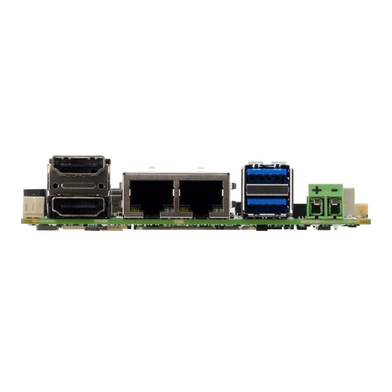
List of Connectors Please refer to the table below for all of the board’s connectors that you can configure for your application Label Function RTC Battery Connector LVDS Back Light Inverter LVDS/eDP [Reserved] Dual HDMI Dual RJ45 SATA SATA Power 4-bit DIO Header USB 2.0/3.2 GEN 2 Port1~Port2 CN10... -
Page 27: Rtc Battery Connector (Cn1)
2.4.1 RTC Battery Connector (CN1) Pin Name Signal Type Signal Level +3.3V +3.3V 2.4.2 LVDS Back Light Inverter (CN2) Pin Name Signal Type Signal Level BLK_PWR +12V (Default)/ +5V BLK_PWR +12V (Default)/ +5V BKL_CONTROL BKL_ENABLE +3.3V Chapter 2 – Hardware Information... -
Page 28: Lvds/Edp [Reserved] (Cn3)
Note 1: Backlight Power can be 12V or 5V, set by BOM: SKU R466 for 12V and SKU R2679 for 5V (Default is 12V). Note 2: CN2 max current 2A. 2.4.3 LVDS/eDP [Reserved] (CN3) Pin Name Signal Type Signal Level LVD1_CB_3_DP DIFF LVD1_CB_3_DN... - Page 29 Pin Name Signal Type Signal Level +V3P3S +3.3V LVD1_DDC_CLK/ Signal DDI0_HPD LVD1_BKLTEN/ Signal DDI0_BKLTEN LVD1_DDC_DATA Signal LVD1_BKLCTL/ Signal DDI0_BKLTCTL LVD1_CA_CLKP/ DIFF DDI0_AUX_DP LVD1_CA_CLKN/ DIFF DDI0_AUX_DN LVD1_CA_3_DP/ DIFF DDI0_LANE3_DP LVD1_CA_3_DN/ DIFF DDI0_LANE3_DN LVD1_CA_0_DP/ DIFF DDI0_LANE0_DP LVD1_CA_0_DN/ DIFF DDI0_LANE0_DN LVD1_CA_1_DP/ DIFF DDI0_LANE1_DP LVD1_CA_1_DN/ DIFF DDI0_LANE1_DN...
-
Page 30: Dual Hdmi (Cn4)
Pin Name Signal Type Signal Level +VDD +3.3V +VDD +3.3V +VDD +3.3V Note: CN3: VDD power current max: 1.5A. 2.4.4 Dual HDMI (CN4) Pin Name Signal Type Signal Level HDMI_TX2+ DIFF HDMI_TX2- DIFF HDMI_TX1+ DIFF HDMI_TX1- DIFF HDMI_TX0+ DIFF Chapter 2 – Hardware Information... - Page 31 Pin Name Signal Type Signal Level HDMI_TX0- DIFF HDMI_CLK+ DIFF HDMI_CLK- DIFF DDC_CLK DDC_DATA HDMI_HPD HDMI_TX2+ DIFF HDMI_TX2- DIFF HDMI_TX1+ DIFF HDMI_TX1- DIFF HDMI_TX0+ DIFF HDMI_TX0- DIFF HDMI_CLK+ DIFF HDMI_CLK- DIFF DDC_CLK Chapter 2 – Hardware Information...
- Page 32 Pin Name Signal Type Signal Level DDC_DATA HDMI_HPD Chapter 2 – Hardware Information...
-
Page 33: Dual Rj45 (Cn5)
2.4.5 Dual RJ45 (CN5) Pin Name Signal Type Signal Level LAN1_MDI0+ DIFF LAN1_MDI0- DIFF LAN1_MDI1+ DIFF LAN1_MDI1- DIFF LAN1_MDI2+ DIFF LAN1_MDI2- DIFF LAN1_MDI3+ DIFF 1P10 LAN1_MDI3- DIFF LAN1_LED_LNK#_ACT Signal +V3P3A 3.3V LAN1_LED_100# Signal LAN1_LED_1000# Signal LAN2_MDI0+ DIFF LAN2_MDI0- DIFF LAN2_MDI1+ DIFF Chapter 2 –... - Page 34 Pin Name Signal Type Signal Level LAN2_MDI1- DIFF LAN2_MDI2+ DIFF LAN2_MDI2- DIFF LAN2_MDI3+ DIFF 2P10 LAN2_MDI3- DIFF LAN2_LED_LNK#_ACT Signal +V3P3A 3.3V LAN2_LED_100# Signal LAN2_LED_1000# Signal Chapter 2 – Hardware Information...
-
Page 35: Sata Port (Cn6)
2.4.6 SATA Port (CN6) Pin Name Signal Type Signal Level SATA_1_TXP DIFF SATA_1_TXN DIFF SATA_1_RXN DIFF SATA_1_RXP DIFF 2.4.7 +5V SATA Power Connector (CN7) Pin Name Signal Type Signal Level +V5S Note: CN7 SATA Power max current 1.5A. Chapter 2 – Hardware Information... -
Page 36: Dio 4-Bit Header (Cn8)
2.4.8 DIO 4-bit Header (CN8) Pin Name Signal Type Signal Level +V5S DIO_0 Signal DIO_1 Signal DIO_2 Signal DIO_3 Signal Note: CN8 DIO power max current: 0.5A. Chapter 2 – Hardware Information... -
Page 37: Usb 2.0/3.2 Gen 2 Port1~Port2 (Cn9)
2.4.9 USB 2.0/3.2 GEN 2 Port1~Port2 (CN9) Pin Name Signal Type Signal Level +V5A_USB12 USB2_0_DN DIFF USB2_0_DP DIFF USB3_0_RXN DIFF USB3_0_RXP DIFF USB3_0_TXN DIFF USB3_0_TXP DIFF +V5A_USB12 USB2_1_DN DIFF USB2_1_DP DIFF USB3_1_RXN DIFF USB3_1_RXP DIFF Chapter 2 – Hardware Information... -
Page 38: Usb 2.0 Dual Port Header (Cn10)
Pin Name Signal Type Signal Level USB3_1_TXN DIFF USB3_1_TXP DIFF Note: CN9 USB Power max current: 2.0A, 1.0A for each port. 2.4.10 USB 2.0 Dual Port Header (CN10) Pin Name Signal Type Signal Level +V5A_USB34 +V5A_USB34 USB2_2_DN DIFF USB2_3_DN DIFF USB2_2_DP DIFF USB2_3_DP... -
Page 39: Msata/ Mini Card Slot (Cn11)
2.4.11 mSATA/ Mini Card Slot (CN11) Pin Name Signal Type Signal Level PCIE_WAKE# +3.3V +3.3V +1.5V +1.5V PCIE_CLK_REQ# PCIE_REF_CLK- DIFF PCIE_REF_CLK+ DIFF Chapter 2 – Hardware Information... - Page 40 Pin Name Signal Type Signal Level W_DISABLE# +3.3V PCIE_RST# +3.3V PCIE_RX-/SATA_RX+ DIFF +3.3V +3.3V PCIE_RX+/SATA_RX- DIFF +1.5V +1.5V SMB_CLK +3.3V PCIE_TX-/SATA_TX- DIFF SMB_DATA +3.3V PCIE_TX+/SATA_TX+ DIFF USB_D- DIFF USB_D+ DIFF +3.3V +3.3V +3.3V +3.3V Chapter 2 – Hardware Information...
-
Page 41: E-Key Slot (Cn12)
Pin Name Signal Type Signal Level +1.5V +1.5V +3.3V +3.3V 2.4.12 M.2 E-Key Slot (CN12) Pin Name Signal Type Signal Level +V3P3A 3.3V USB2_4_DP DIFF +V3P3A 3.3V USB2_4_DN DIFF Chapter 2 – Hardware Information... - Page 42 Pin Name Signal Type Signal Level PCIE_2_TXP DIFF PCIE_2_TXN DIFF Chapter 2 – Hardware Information...
- Page 43 Pin Name Signal Type Signal Level PCIE_2_RXP DIFF PCIE_2_RXN PCIE_0_CLK_DP DIFF PCIE_0_CLK_DN DIFF BUF_PLT_RST# Signal PCIE_CLKREQ#0 Signal SOC_BT_EN Signal PCIE_WAKE# Signal SOC_WIFI_EN Signal Chapter 2 – Hardware Information...
-
Page 44: Can Bus Dual Port Header (Cn13)
Pin Name Signal Type Signal Level +V3P3A 3.3V +V3P3A 3.3V 2.4.13 CAN Bus Dual Port Header (CN13) Pin Name Signal Type Signal Level +V5A +V3P3A +3.3V CAN_BUS0_H CAN_BUS0_L CAN_BUS1_H CAN_BUS1_L Chapter 2 – Hardware Information... -
Page 45: Com Dual Port Header (Cn15)
2.4.14 COM Dual Port Header (CN15) RS232 Signal RS422 Signal RS485 Signal DCD_1 TX_1- DATA_1- DCD_2 TX_2- DATA_2- RX_1 TX_1+ DATA_1+ RX_2 TX_2+ DATA_2+ TX_1 RX_1+ TX_2 RX_2+ DTR_1 RX_1- DTR_2 RX_2- DSR_1 DSR_2 RTS_1 RTS_2 CTS_1 CTS_2 RI_1/12V/5V RI_2/12V/5V Chapter 2 –... -
Page 46: Spi Port (Cn17)
RS232 Signal RS422 Signal RS485 Signal UART_TX UART_RX Note 1: COM RS-232/ 422/ 485 mode can be set by BIOS. Default is RS-232. Note 2: RI1/+5V/+12V can be set by BOM (R423 RI/ R369 +12V/ R370 +5V). Default is RING. Note 3: RI2/+5V/+12V can be set by BOM (R424 RI/ R372 +12V/ R373 +5V). -
Page 47: Espi/ Smbus/ I2C (Cn18)
2.4.16 eSPI/ SMBus/ I2C (CN18) Pin Name Signal Type Signal Level ESPI_IO0 IN/OUT +1.8V ESPI_IO1 IN/OUT +1.8V ESPI_IO2 IN/OUT +1.8V ESPI_IO3 IN/OUT +1.8V +V3.3S +3.3V ESPI_CS Signal ESPI_RESET# +1.8V ESPI_CLK 1.8V SMB_DATA/ I2C_SDA IN/OUT +3.3V SMB_CLK/ I2C_CLK +3.3V SMB_ALERT/ +3.3V INT_SERIRQ Chapter 2 –... -
Page 48: 4-Pin Smart Fan Connector (Cn19)
2.4.17 4-pin Smart Fan Connector (CN19) Pin Name Signal Type Signal Level +V12S +12V FAN_TAC Signal FAN_CTL Signal Note: CN19 Smart Fan power max current: 1.0A. 2.4.18 Power Input +12V (CN20) Pin Name Signal Type Signal Level +V_IN +12V Chapter 2 – Hardware Information... -
Page 49: Front Panel (Cn21)
2.4.19 Front Panel (CN21) Pin Name Signal Type Signal Level EXT_PWRBTN# Signal FP_IDELED# Signal +V3P3S +3.3V FP_BUZZER Signal +V5S +V3P3S +3.3V HWRST# Signal Chapter 2 – Hardware Information... -
Page 50: Dc Jack Power Input [Reserved] (Cn22)
2.4.20 DC Jack Power Input [Reserved] (CN22) Pin Name Signal Type Signal Level +V_IN +12V Chapter 2 – Hardware Information... -
Page 51: Single Rj45 [Reserved] (Cn23)
2.4.21 Single RJ45 [Reserved] (CN23) Pin Name Signal Type Signal Level LAN1_MDI0+ DIFF LAN1_MDI0- DIFF LAN1_MDI1+ DIFF LAN1_MDI1- DIFF LAN1_MDI2+ DIFF LAN1_MDI2- DIFF LAN1_MDI3+ DIFF 1P10 LAN1_MDI3- DIFF LAN1_LED_LNK#_ACT Signal +V3P3A 3.3V LAN1_LED_100# Signal LAN1_LED_1000# Signal Chapter 2 – Hardware Information... -
Page 52: Thermal Assembly Options
Thermal Assembly Options 2.5.1 Active Cooling Fan FAN01 Active Cooling Fan, Part Number: PICO-EHL4-FAN01 Chapter 2 – Hardware Information... -
Page 53: Fan-Less Heatspreader Hsp01
2.5.2 Fan-less Heatspreader HSP01 Heat spreader/ fan-less assembly, Part Number: PICO-EHL4-HSP01 Chapter 2 – Hardware Information... -
Page 54: Heatsink Hsk01 (With Heatspreader)
2.5.3 Heatsink HSK01 (with Heatspreader) Heatsink with heatspreader, Part Number: PICO-EHL4-HSK01 Chapter 2 – Hardware Information... -
Page 55: Chapter 3 - Ami Bios Setup
Chapter 3 Chapter 3 - AMI BIOS Setup... -
Page 56: System Test And Initialization
System Test and Initialization These routines test and initialize board hardware. If the routines encounter an error during the tests, you will either hear a few short beeps or see an error message on the screen. There are two kinds of errors: fatal and non-fatal. The system can usually continue the boot up sequence with non-fatal errors. -
Page 57: Ami Bios Setup
AMI BIOS Setup AMI BIOS ROM has a built-in Setup program that allows users to modify the basic system configuration. This type of information is stored in battery-backed CMOS RAM and BIOS NVRAM so that it retains the Setup information when the power is turned off. Entering Setup Power on the computer and press <Del>or <ESC>... -
Page 58: Setup Submenu: Main
Setup Submenu: Main Chapter 3 – AMI BIOS Setup... -
Page 59: Setup Submenu: Advanced
Setup Submenu: Advanced Chapter 3 – AMI BIOS Setup... -
Page 60: Cpu Configuration
3.4.1 CPU Configuration Options Summary Active Processor Cores Optimal Default, Failsafe Default Number of cores to enable in each processor package. Intel (VMX) Virtualization Disabled Technology Enabled Optimal Default, Failsafe Default When enabled, a VMM can utilize the additional hardware capabilities provided by Vanderpool Technology. -
Page 61: Pch-Fw Configuration
3.4.2 PCH-FW Configuration Chapter 3 – AMI BIOS Setup... -
Page 62: Firmware Update Configuration
3.4.2.1 Firmware Update Configuration Options Summary Me FW Image Re-Flash Enabled Disabled Optimal Default, Failsafe Default Enable/Disable Me FW Image Re-Flash function. FW Update Disabled Enabled Optimal Default, Failsafe Default Enable/Disable ME FW Update function. Chapter 3 – AMI BIOS Setup... -
Page 63: Trusted Computing
3.4.3 Trusted Computing Options Summary Security Device Support Enable Optimal Default, Failsafe Default Disable Enables or Disables BIOS support for security device. O.S. will not show Security Device. TCG EFI protocol and INT1A interface will not be available. SHA-1 PCR Bank Disabled Optimal Default, Failsafe Default Enabled... - Page 64 Options Summary SM3_256 PCR Bank Enabled Optimal Default, Failsafe Default Disabled Enable or Disable SM3_256 PCR Bank Pending operation None Optimal Default, Failsafe Default TPM Clear Schedule an Operation for the Security Device. NOTE: Your Computer will reboot during restart in order to change State of Security Device. Platform Hierarchy Enabled Optimal Default, Failsafe Default...
-
Page 65: Sata Configuration
3.4.4 SATA Configuration Options Summary SATA Controller(s) Enabled Optimal Default, Failsafe Default Disabled Enable/Disable SATA Device. Port* Enabled Optimal Default, Failsafe Default Disabled Enable or Disable SATA Port. Chapter 3 – AMI BIOS Setup... -
Page 66: Sdio Configuration
3.4.5 SDIO Configuration Options Summary eMMC 5.1 Controller Enabled Optimal Default, Failsafe Default Disabled Enable or Disable SCS eMMC 5.1 Controller SDIO Access Mode Auto Optimal Default, Failsafe Default ADMA SDMA Auto Option: Access SD device in DMA mode if controller supports it, otherwise in PIO mode. -
Page 67: Hardware Monitor
3.4.6 Hardware Monitor Chapter 3 – AMI BIOS Setup... -
Page 68: Smart Fan Mode Configuration
3.4.6.1 Smart Fan Mode Configuration Options Summary Fan1 Output Mode Output PWM mode (open drain) Output PWM mode (push Optimal Default, Failsafe Default pull) Output PWM mode (push pull) to control 4-wire fans. Linear fan application circuit to control 3-wire fan speed by fan’s power terminal. Output PWM mode (open drain) to control Intel 4-wire fans. -
Page 69: Sio Configuration
3.4.7 SIO Configuration Chapter 3 – AMI BIOS Setup... -
Page 70: Serial Port Configuration
3.4.7.1 Serial Port Configuration Options Summary Use This Device Disabled Enabled Optimal Default, Failsafe Default Enable or Disable Serial Port (COM) Possible: Use Automatic Settings Optimal Default, Failsafe Default IO=2F8; IRQ=3; IO=3F8; IRQ=4; Select an optimal setting for IO device Mode RS232 Optimal Default, Failsafe Default... -
Page 71: Aaeon Bios Robot
3.4.8 AAEON BIOS Robot Options Summary Sends watch dog Disabled Optimal Default, Failsafe Default before BIOS POST Enabled Enabled - Robot set Watch Dog Timer (WDT) right after power on, before BIOS start POST process. And then Robot will clear WDT on completion of POST. WDT will reset system automatically if it is not cleared before its timer counts down to zero. - Page 72 Enabled - Robot set Watch Dog Timer (WDT) after POST completion, before BIOS transfer control to OS. WARNING: Before enabling this function, a program in OS must be in responsible for clearing WDT. Also, this function should be disabled if OS is going to update itself.
-
Page 73: Power Management
3.4.9 Power Management Options Summary Power Mode ATX Type Optimal Default, Failsafe Default AT Type Select power supply mode. Restore AC Power Last State Optimal Default, Failsafe Default Loss Always On Always Off Select power state when power is re-applied after a power failure. RTC wake system Disabled Optimal Default, Failsafe Default... -
Page 74: Digital Io Port Configuration
3.4.10 Digital IO Port Configuration Options Summary DIO Port0~3 Output Optimal Default, Failsafe Default Input Set DIO as Input or Output Output Level High Optimal Default, Failsafe Default Set output level when DIO pin is output Chapter 3 – AMI BIOS Setup... -
Page 75: Setup Submenu: Chipset
Setup Submenu: Chipset Chapter 3 – AMI BIOS Setup... -
Page 76: System Agent (Sa) Configuration
3.5.1 System Agent (SA) Configuration Chapter 3 – AMI BIOS Setup... -
Page 77: Memory Configuration
3.5.1.1 Memory Configuration Chapter 3 – AMI BIOS Setup... -
Page 78: Graphics Configuration
3.5.1.2 Graphics Configuration Options Summary Internal Graphics Auto Optimal Default, Failsafe Default Disabled Enabled Keep IGFX enabled based on the setup options. Chapter 3 – AMI BIOS Setup... - Page 79 3.5.1.2.1 LVDS Panel Configuration Options Summary LVDS Disabled Enabled Optimal Default, Failsafe Default Enable/Disable this panel. LVDS Panel Type 640X480@60HZ 800X480@60HZ 800X600@60HZ 1024X600@60HZ 1024X768@60HZ Optimal Default, Failsafe Default 1280X768@60HZ 1280X800@60HZ 1280X1024@60HZ 1366X768@60HZ 1440X900@60HZ Select panel type Chapter 3 – AMI BIOS Setup...
- Page 80 Options Summary Color Depth 18-bit Optimal Default, Failsafe Default 24-bit Select Color Depth Backlight Mode Windows Slider Optimal Default, Failsafe Default BIOS & Application Select backlight control signal type Backlight Type Normal Optimal Default, Failsafe Default Inverted Select backlight control signal type Backlight Level Optimal Default, Failsafe Default 100%...
-
Page 81: Pch-Io Configuration
3.5.2 PCH-IO Configuration Options Summary HD Audio Enabled Optimal Default, Failsafe Default Disabled Control Detection of the HD-Audio device. Disabled = HDA will be unconditionally disabled Enabled = HDA will be unconditionally enabled. Full-MiniCard Slot SATA Optimal Default, Failsafe Default Function (CN11) PCIe Select function enabled for Full-MiniCard (CN11) Slot... -
Page 82: Setup Submenu: Security
Setup Submenu: Security Change User/Supervisor Password You can install a Supervisor password, and if you install a supervisor password, you can then install a user password. A user password does not provide access to many of the features in the Setup utility. If you highlight these items and press Enter, a dialog box appears which lets you enter a password. -
Page 83: Secure Boot
3.6.1 Secure Boot Options Summary Secure Boot Disabled Optimal Default, Failsafe Default Enabled Secure Boot feature is Active if Secure Boot is Enabled, Platform Key (PK) is enrolled and the System is in User mode. The mode change requires platform reset Secure Boot Mode Standard Custom... -
Page 84: Key Management
3.6.1.1 Key Management Options Summary Factory Key Provision Disabled Optimal Default, Failsafe Default Enabled Install factory default Secure Boot keys after the platform reset and while the System is in Setup mode Restore Factory Keys Force System to User Mode. Install factory default Secure Boot key databases Reset To Setup Mode Delete all Secure Boot key databases from NVRAM Export Secure Boot variables... - Page 85 Options Summary Remove 'UEFI CA' from DB Device Guard ready system must not list 'Microsoft UEFI CA' Certificate in Authorized Signature database (db) Restore DB defaults Restore DB variable to factory defaults Secure Boot Variables Enroll Factory Defaults or load certificates from a file: 1.
-
Page 86: Setup Submenu: Boot
Setup Submenu: Boot Options Summary Quiet Boot Disabled Enabled Optimal Default, Failsafe Default Enable or Disable Quiet Boot option. Network Stack Disabled Optimal Default, Failsafe Default Enabled Enable/Disable UEFI Network Stack. IPv4 PXE Support Disabled Optimal Default, Failsafe Default Enabled Enable/Disable IPv4 PXE boot support. -
Page 87: Setup Submenu: Save & Exit
Setup Submenu: Save & Exit Options Summary Save Changes and Reset Reset the system after saving the changes. Discard Changes and Exit Exit system setup without saving any changes. Restore Defaults Restore/Load Default values for all the setup options. Chapter 3 – AMI BIOS Setup... -
Page 88: Chapter 4 - Drivers Installation
Chapter 4 Chapter 4 – Drivers Installation... -
Page 89: Drivers Download And Installation
Drivers Download and Installation Drivers for the PICO-EHL4-A11 can be downloaded from the product page on the AAEON website by following this link: https://www.aaeon.com/en/p/pico-itx-turnkit-pico-ehl4 Download the driver(s) you need and follow the steps below to install them. Step 1 – Install Chipset Driver Open the Intel Chipset folder. - Page 90 Step 4 – Install ME Driver Open the ME folder. Run the SetupME.exe file Follow the instructions Driver will be installed automatically Step 5 – Install LAN Driver Open the LAN folder. Run the Install_Win10_10050_08132021.exe file Follow the instructions Driver will be installed automatically Step 6 –...
-
Page 91: Appendix A - Mating Connectors
Appendix A Appendix A – Mating Connectors... -
Page 92: List Of Mating Connectors And Cables
List of Mating Connectors and Cables The following table lists mating connectors and available cables. Mating Connector Connector Available AAEON Function Label Cable Cable P/N Vendor Model no RTC Battery Molex 51021-0200 Battery 175011301C Cable LVDS Back Light WL1010H-6P LVDS 170X000152 Inverter Terminal: KB901-10T... - Page 93 Mating Connector Connector Available AAEON Function Label Cable Cable P/N Vendor Model no CN21 Front Panel ACES 50247-010H0H0-001 Front Panel 1709100108 Cable CN22 DC Jack Power HUANG 5525C257-3T00-R1-7.5 Power 1702041004 Input Cable Note 1: eDP Test Panel: B173ZAN01.0-AUO & LVDS Test Panel: G121XN01V0-AUO. Note 2: 170X000531 (TF)EDP Cable.40P .with AUO B173ZAN01.0.300mm.UC Function.UC-W037.For PICO-EHL4 A1.1.
-
Page 94: Appendix B - I/O Information
Appendix B Appendix B - I/O Information... -
Page 95: Direct Memory Access (Dma) Map
Direct Memory Access (DMA) Map Appendix B – I/O Information... -
Page 96: I/O Address Map
I/O Address Map Appendix B – I/O Information... -
Page 97: Irq Mapping Chart
IRQ Mapping Chart Appendix B – I/O Information... - Page 98 Appendix B – I/O Information...
- Page 99 Appendix B – I/O Information...
- Page 100 Appendix B – I/O Information...
- Page 101 Appendix B – I/O Information...
- Page 102 Appendix B – I/O Information...
- Page 103 Appendix B – I/O Information...
- Page 104 Appendix B – I/O Information...
- Page 105 Appendix B – I/O Information...
- Page 106 Appendix B – I/O Information...
- Page 107 Appendix B – I/O Information...
-
Page 108: Large Memory Map
Large Memory Map Appendix B – I/O Information... -
Page 109: Memory Address Map
Memory Address Map Appendix B – I/O Information... - Page 110 Appendix B – I/O Information...
-
Page 111: Appendix C - Watchdog Timer Programming
Appendix C Appendix C - Watchdog Timer Programming... -
Page 112: Introduction To Watchdog Timer
Introduction to Watchdog Timer This section details how to set up and program the Watchdog Timer for your AAEON system or board. The watchdog timer is used to automatically detect malfunctions and recover the system. During normal operation, the system will regularly send a signal to reset the watchdog timer. -
Page 113: C.2 Programing The Watchdog Timer With Aaeon Sdk
C.2 Programing the Watchdog Timer with AAEON SDK If you have installed the AAEON Framework, you can program the Watchdog Timer using the AAEON SDK. Simply locate where the SDK is installed, and double click the icon. The following dialog box will appear: Count Mode: Set Watchdog Timer to count in minutes or seconds. -
Page 114: C.3 Programing Watchdog Timer With Aaeon Windows Eapi
C.3 Programing Watchdog Timer with AAEON Windows EAPI AAEON Framework (KMDF Driver) must be installed before calling these functions. EapiLibInitialize() should be the first to call before calling other EAPI functions. EApiLibUnInitialize() should be called to release resources before program exit. When building C/C++ apps, Lib (Library, aaeonEAPI.lib) is needed. -
Page 115: Watchdog Timer Functions
EApiWDogStop must be called before Stage D/G to prevent system from being reset. C.3.1 Watchdog Timer Functions C.3.1.1 EapiWDogGetCap() Command Line: EApiWDogGetCap(…) __OUTOPT uint32_t *pMaxDelay, __OUTOPT uint32_t *pMaxEventTimeout, __OUTOPT uint32_t *pMaxResetTimeout Use this command to get maximum Supported Delay / Supported Event Timeout / Supported Reset Timeout of the watchdog timer. -
Page 116: Eapiwdogstart()
C.3.1.2 EapiWDogStart() Command Line: EApiWDogStart( __IN uint32_t Delay, __IN uint32_t Minute, __IN uint32_t EventTimeout, __IN uint32_t ResetTimeout Use this command to start the Watchdog Timer and set the timeout values. To stop the Watchdog Timer, issue the command EApiWDogStop. After issuing EAPiWDogStop, the command EApiWDogStart must be called again with new values to restart. -
Page 117: Eapiwdogtrigger()
C.3.1.3 EapiWDogTrigger() Command Line: EapiWDogTrigger() Use this command to trigger the Watchdog Timer. Parameters Function Parameters None Condition Return Values Library Uninitialized EAPI_STATUS_NOT_INITIALIZED Watchdog Not Started EAPI_STATUS_ERROR Common Error Common Error Code Others EAPI_STATUS_SUCCESS C.3.1.4 EapiWDogStop() Command Line: EapiWDogStop() Use this command to close the Watchdog Instance. This will disable the Watchdog Timer and clear previous settings. -
Page 118: Eapiwdogreloadtimer()
C.3.1.5 EapiWDogReloadTimer() Command Line: EapiWDogReloadTimer() Use this command to reload the Timeout count Parameters Function Parameters None Condition Return Values Library Uninitialized EAPI_STATUS_NOT_INITIALIZED Common Error Common Error Code Others EAPI_STATUS_SUCCESS C.3.1.6 EapiWDogGetStatus() Command Line: EapiWDogGetStatus( __OUTOPT uint32_t *pwdtMinute, __OUTOPT uint32_t *pwdtCountTime, __OUTOPT uint32_t *pwdtReloadTime Use this command to get the Watchdog Timer mode, time count value and reload timer. - Page 119 C.3.1.7 EapiWDogSetStatus() Command Line: EApiWDogSetStatus( __IN uint32_t wdtMinute, __IN uint32_t wdtCountTime, __IN uint32_t wdtReloadTime Use this command to set Watchdog Timer mode, time count value and reload timer. Parameters Function Parameters wdtMinute Set the mode of minute or second wdtCountTime Set WDT time count wdtReloadTime Set WDT ReloadTime...