Table of Contents
Advertisement
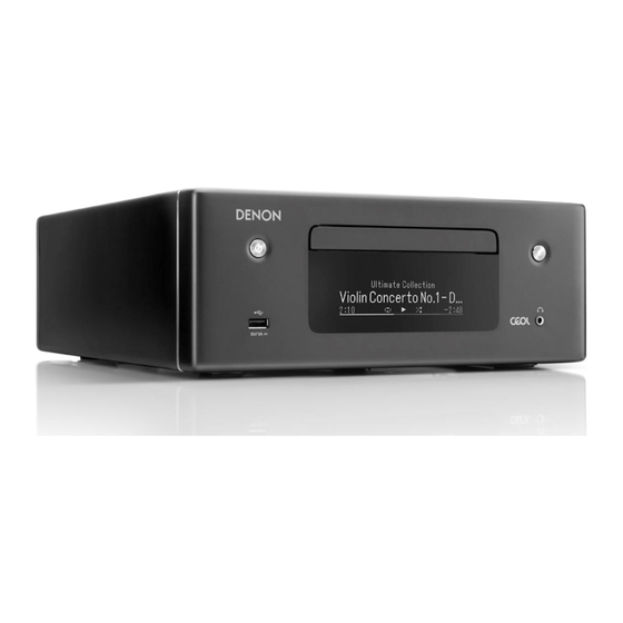
NETWORK CD RECEIVER
RCD-N10
• For purposes of improvement, specifications and design are subject to change without notice.
• Please use this service manual when referring to the operating instructions without fail.
• Some illustrations used in this service manual are slightly different from the actual product.
Service Manual
Click here!
On-line service parts list
http://dmedia.dmglobal.com/Document/DocumentDetails/24852
ONLINE PARTS LIST
(P5)
WEB owner's manual
NA:
http://manuals.denon.com/RCDN10/NA/EN/index.php
EU:
http://manuals.denon.com/RCDN10/EU/EN/index.php
AP:
http://manuals.denon.com/RCDN10/AP/ZH/index.php
JP:
http://manuals.denon.com/RCDN10/JP/JA/index.php
Upload is planned for the time of a future press release.
BEFORE SERVICING THIS UNIT
ELECTRICAL
MECHANICAL
REPAIR INFORMATION
UPDATING
Confidential
Ver. 1
Advertisement
Table of Contents

Related Manuals for Denon RCD-N10


Summary of Contents for Denon RCD-N10
- Page 1 Service Manual Ver. 1 NETWORK CD RECEIVER RCD-N10 Click here! On-line service parts list http://dmedia.dmglobal.com/Document/DocumentDetails/24852 ONLINE PARTS LIST (P5) WEB owner’s manual http://manuals.denon.com/RCDN10/NA/EN/index.php http://manuals.denon.com/RCDN10/EU/EN/index.php http://manuals.denon.com/RCDN10/AP/ZH/index.php http://manuals.denon.com/RCDN10/JP/JA/index.php Upload is planned for the time of a future press release. BEFORE SERVICING THIS UNIT...
- Page 2 BEFORE SERVICING THIS UNIT SAFETY PRECAUTIONS NOTE FOR SCHEMATIC DIAGRAM HANDLING THE SEMICONDUCTOR AND OPTICS WARNING AND LASER SAFETY INSTRUCTIONS ONLINE PARTS LIST Accessing the Parts List Searching Part Numbers or Ref. Numbers NOTE FOR PARTS LIST SERIAL NUMBER Serial Number Organization SKU Code of this Unit POST-SERVICE PRECAUTIONS Initializing this Unit...
-
Page 3: Safety Precautions
SAFETY PRECAUTIONS The following items should be checked for continued protection of the customer and the service technician. Leakage current check Before returning the set to the customer, be sure to carry out either (1) a leakage current check or (2) a line to chassis resistance check. If the leakage current exceeds 0.5 milliamps, or if the resistance from chassis to either side of the power cord is less than 460 kohms, the set is defective. -
Page 4: Note For Schematic Diagram
NOTE FOR SCHEMATIC DIAGRAM WARNING AND LASER SAFETY INSTRUCTIONS WARNING: WARNING WAARSCHUWING Parts indicated by the z mark have critical characteristics. Use ONLY replacement parts recommended Alle IC’s en vele andere halfgeleiders zijn gevoelig All ICs and many other semi-conductors are voor elektrostatische ontladingen (ESD). -
Page 5: Note For Parts List
ONLINE PARTS LIST Accessing the Parts List Searching Part Numbers or Ref. Numbers (1) Access from the Service Manual You can search a Parts List for part numbers or Ref. numbers. ・ Click the URL link on the cover of the service manual. (1) Enter the part number or Ref. - Page 6 SERIAL NUMBER Serial Number Organization The 14-digit serial number that contains the code of the manufacturing plant and the manufacturing date. 14 digits Factory Manufactured Cumulative Year, month code code serial number The last Month 2digit of year (01 ~ 12) SKU Code of this Unit Product SKU SKU Code...
-
Page 7: Initializing This Unit
POST-SERVICE PRECAUTIONS Initializing this Unit Make sure to initialize this unit after replacing the microcomputer or any peripheral equipment, or the PCB. 1. Press the power operation button to turn off the power, and remove the AC plug from the socket. 2. -
Page 8: Schematic Diagrams
ELECTRICAL SCHEMATIC DIAGRAMS SCH01 MCU SCH02 DIR SCH03 PWM SCH04 NETWORK SCH05 CD DSP SCH06 DAMP SCH07 FRONT INPUT SCH08 SMPS SCH09 Touch Function PRINTED CIRCUIT BOARDS MAIN, HEADPHONE, AC-IN, USB, SUPPORT DAMP, CD, NETWORK FRONT, OPTICAL, SMPS BLOCK DIAGRAM POWER DIAGRAM WIRING DIAGRAM SEMICONDUCTORS... - Page 9 SCHEMATIC DIAGRAMS SCH01 MCU PF60 From LEGO PCB TO WF60 PF60 CJP23GA117ZY CN93 CN93 OLED_P_CONT (PAGE 2_D4) *** Please design capacitors near the MCU IC's VCC Pin. TO 2A +3.3V_CPU CJP13GI236ZW (PAGE 2_B5) BURST_CONT (PAGE 4_B6) (PAGE 2_B5) SUB_PWR_CONT P_DOWN DGND +12V IC26...
- Page 10 SCH02 DIR TO 4A TO TAS5558 FROM PF60 (FROM LEGO) (PAGE 2_D5) (PAGE 4_A5) (PAGE 2_D5) 100P C241 100P BN16 C240 From INPUT 100P C239 100P D233 TO CN16 C238 1N4148 BN16 IC31 LM317DCYR-ADJ CWB1B00508047002 +3.3VD Q210 RT1P141C +3.3VD IC33 +7.5VA DGND L201 60...
- Page 11 SCH03 PWM Q201 RT1P141C D203 SW_MUTE 0.01 CUP12955Z-3 C250 +12VD C251 1SS355T HeadPhone D207 Q238 C252 MTA50P01SN3 +5VS C259 L218 1SS355T +12V CVD1SS355T D217 R235 DGND L208 JK11 Q219 CVD1SS355T D218 +12VD RT1P141C CJJ2D051ZD BN10 HP12V_SW -12VD EMI CM CHGND_4 AGND_4 1SS355T 1SS355T...
- Page 12 SCH04 NETWORK FROM LEGO M ODULE LEGO AOUT DIST AIN ETHERNET CN111 CN112 CJP80GA370ZU CJP42GA370ZU T110 LEGO5V DGND NET3.3V C1138 0.1uF BK110 BK111 BK112 BK113 BK114 BK115 BK116 AIOS4_MCLK_I2S_O R1155 AIOS4_MCLKO IC113 CVISN74LV1T125DBVR R1179 R1178 R1177 R1176 R1175 R1174 R1173 R1102 WF60 R1172...
- Page 13 SCH05 CD DSP TO CD PICKUP 0.01 C827 CD DSP PARTS C815 C892 C850 10V/470uF L803 C851 R833 1000P C814 C808 10uH R834 0.01 C817 C891 C810 Q800 R835 10V/470uF A1504S R836 0.01 C826 GND_DRV GND_DRV C812 C811 C852 C884 C813 C816 0.01...
- Page 14 SCH06 DAMP D-AMP C753 EMI CM_0322 16V/100uF R734 R735 C757 50V/3300uF Toshin CAP C733 IC70 22uF TAS5142DKD 22uF C734 DGND WF70 WF70 C700 TO PF70 GVDD_B C701 0.1 GVDD_A C749 33N(20) R715 C737 BST_A L708 R707 3216, 10uF/50V DGND PVDD_A CLZ9Z189Z PWM_A DGND...
- Page 15 SCH07 FRONT INPUT WF11 FRONT<=>MAIN(MCU) TO PF11 W F11 CJP31G B286ZN TUNER&Optical R122 CUP12954Z-1 CUP12954Z-2 R115 RC11 T M11 R303SC5C L110 FRONT 50V/10uF 60ohm C104 L_OUT WF15 L111 CJP11GA115ZY 60ohm C105 50V/10uF R_OUT W F15 L107 L112 L106 Q108 60ohm TU+ 5V OPEN 10uH...
- Page 16 SCH08 SMPS D939 IC93 Q933 7812A 2SA2167ES L927 L929 PT91 +16V_OLED CN91 CN91 [2.5 MM] 0 ohm CLZ9R001Z CLZ9R001Z +29V R951 +29V TO BN91 DGND DGND +29V BD98 C922 L921 HS92 For D925 HEAT SINK 1KV 471 J 100MHz_60ohm_5A DGND 100MHz_60ohm_5A TH91 L924...
- Page 17 SCH09 Touch Function 9 CHANNEL Touch PAD +3.3VD TC[01:09] +3.3VD TC01 (ENTER) TC02 (UP) 10022HS-07C02 CN1_ TC03 (DOWN) 1.+3.3VD 2.+3.3VD TC04 (LEFT) TC390_MLF32 3.TS_I2C_SCL +3.3VD 4.TS_I2C_SDA TC05 (RIGHT) TS_I2C_SDA 5.TS_INT TS_INT TC[01:09] 6.DGND TC06 (BACK) TS_I2C_SCL 7.DGND TC07 (INPUT) CONNECTOR TO WF13 +3.3VD TC08...
-
Page 18: Printed Circuit Boards
PRINTED CIRCUIT BOARDS MAIN, HEADPHONE, AC-IN, USB, SUPPORT Lead-free Solder When soldering, use the Lead-free Solder (Sn-Ag-Cu). USB (A SIDE) USB (B SIDE) AC-IN (A SIDE) AC-IN (B SIDE) HEADPHONE (A SIDE) HEADPHONE (B SIDE) CUP12955Z-3 F901 JK11 JK90 JK60 LF92 LF91 CUP12955Z-4... - Page 19 DAMP, CD, NETWORK CD (A SIDE) CD (B SIDE) D-AMP (A SIDE) D-AMP (B SIDE) FCT1 FCT2 DGND C819 C879 C843 R847 C845 R849 CUP12950Z MP C837 R809 R807 C896 C868 R817 R808 C836 R831 R812 R848 R866 C889 C862 C805 C871 C905...
- Page 20 FRONT, OPTICAL, SMPS FRONT (A SIDE) FRONT (B SIDE) J140 Q101 WF11 WF13 D102 D105 DGND J141 S102 DGND DGND J148 Q105 DGND POWER S101 OPEN/CLOSE POWER J142 OPEN/CLOSE DGND DGND GND2 J127 J154 L114 J123 J144 J153 J122 L115 J138 DGND DGND...
-
Page 21: Block Diagram
BLOCK DIAGRAM Touch Sensor &LED Display Module FRONT B'D LED表示部 SWITCHED-MODE POWER SUPPLY Volume + INPUT ↓ Enter ↑ → ← Power LED (White) Volume - BACK Status LED (Red, Orange) Eject LED (white) Touch Sensor Pad部 RC IN BACK INPUT OLED Pioneer... -
Page 22: Power Diagram
POWER DIAGRAM SUB POWER CONT (Power-H) IC80 NJM7808FA Regulator IC99 7812A +12V D-amp +12V +12V +12V H/P&SW AMP,Mute IC31 LM317 +7.5V +7.5V AudioSelecto r,Amp IC98 KIA79L12BP -12V -12V -12V H/P&SW AMP,Mute IC32 LM337 SMPS -7.5V Trans -7.5V AudioSelecto r,Amp OLED POWER +29V +29V D-amp... -
Page 23: Wiring Diagram
WIRING DIAGRAM WF70 (6PIN, B to B) WF71 (6PIN, B to B) TUNER & OPT JACK PCB CJP06GA413ZDE CJP06GA413ZDE CUP12954Z-2 FILTER OPT JACK1 3.96 PITCH CJP02KA060ZY CN90 (2PIN, WAFER) OPT JACK2 WF72 (12PIN, B to B) WF15 (11PIN,FFC WAFER) CJP12GA413ZDE CJP11GA117ZY TM11 TUNER MODULE... - Page 24 SEMICONDUCTORS Only major semiconductors are shown, general semiconductors etc. are omitted to list. The semiconductor which described a detailed drawing in a schematic diagram are omitted to list. 1. IC's R5F5631FDDFB (MAIN: IC20) Port Name Function Name Nor- Net- Clock Detail of Function STBY work...
- Page 25 Port Name Function Name Nor- Net- Clock Detail of Function Port Name Function Name Nor- Net- Clock Detail of Function STBY work display STBY work display STBY STBY mode STBY STBY mode Power Supply Pin PD3/IRQ3/AN011 CD_BUS3 CD DSP Control Pin (Need to connect the consecutive ports of (IOEXP_INT) reserved (I/O Expander INT) NC (Open) uCOM.)
- Page 26 TC94A92FG (CD: IC83) TC94A92FG (IC17) Symbol Description Default Remarks DVSS3R Grounding pin for 3.3V Muiti-Bit DAC circuit R channel audio output pin of Audio DAC. 3AI/F DVDD3R Power supply pin for 3.3V Audio DAC circuit. DVDD3L Power supply pin for 3.3V Audio DAC circuit. L channel audio output pin of Audio DAC 3AI/F DVSS3L...
- Page 27 Symbol Description Default Remarks Symbol Description Default Remarks VDD3 Power Supply pin for 3.3V Digital circuit CMOS Port VDD3 Power Supply pin for 3.3V Digital circuit Schmitt input BUS0 Microprocessor I/F data input/output pin 0 CMOS Port 3I/F Refer to [1.2 Pin Assinment Table] BUS0 Microprocessor I/F data input/output pin 0 Schmitt input...
- Page 28 BA5810FP/FM 光ディスク IC BA5810 (CD: IC81) BD82065FVJ-E2 (NETWORK: IC112) BD82061FVJ BD82065FVJ ブロックダイアグラム Block Diagram CH1~ POWVCC 34 (CH3, CH4) MUTE 7.5k − − LEVEL 7.5k SHIFT − − LEVEL SHIFT LEVEL LOADING PRE SHIFT FWD REV − LEVEL − 7.5k SHIFT −...
- Page 29 PCM9211 PCM5100APWR (MAIN: IC39) PCM9211 (MAIN: IC37/IC38) PCM5100A, PCM5101A, PCM5102A www.ti.com SBAS495 – JUNE 2010 PCM5100A-Q1, PCM5101A-Q1, PCM5102A-Q1 PIN CONFIGURATIONS www.ti.com SLAS859C – MAY 2012 – REVISED MAY 2015 PT PACKAGE LQFP-48 7 Pin Configuration and Functions (TOP VIEW) PW 20-Pin Package (Top View) ERROR/INT0 VDDRX...
- Page 30 PCM9211 PCM9211 BLOCK DIAGRAM www.ti.com SBAS495 – JUNE 2010 BLOCK DIAGRAM DESCRIPTION NAME FILT TOLERANT AUXIN 0 MS/ADR1 Software control I/F, SPI chip select / I2C slave address AUTO RXIN7 setting1(2) RXIN 0 RXIN0 SCKO DOUT RXIN 1 RXIN1 MAIN OUTPUT MODE Control mode setting, (see the Serial Control Mode section,...
- Page 31 The TAS5142 is available in two thermally enhanced packages: • 36-pin PSOP3 package (DKD) • 44-pin HTSSOP PowerPad™ package (DDV) Both package types contain a heat slug that is located on the top side of the device for convenient thermal coupling to the heatsink.
- Page 32 TAS5558 TAS5142 SLES273A – APRIL 2013 – REVISED JUNE 2013 www.ti.com Device Information www.ti.com Physical Characteristics TAS5142 Block Diagram TAS5558 (MAIN: IC40) SLES126B – DECEMBER 2004 – REVISED MAY 2005 2.1.1 TAS5558 Pin Assignments FUNCTIONAL BLOCK DIAGRAM DCA Package (Top View) PWM_HPM_L PWM_P_6 PWM_HPP_L...
- Page 33 CS (Current Sense) www.ti.com SLES273A – APRIL 2013 – REVISED JUNE 2013 The Current Sense pin senses the voltage developed Package PG-DSO-8 on the series resistor inserted in the source of the These devices have limited built-in ESD protection. The leads should be shorted together or the device placed in conductive foam Power MOSFET.
- Page 34 3 Pin Configuration Pin Assignments & Functions Pin Assignments & Functions NR111E (SMPS: IC95) TC390_MLF32(Touch sensor: U1) Pin Configuration Pin Assignments Pin Functions Pin Assignments 32 31 30 29 28 27 26 25 Pin Functions NR111E Pin Discriptions i r c VDDIO P1.7 / TS1.7...
- Page 35 2. FL DISPLAY MXS4035A MXS4035A IO Interfaces...
- Page 36 00001010 10000111 11000010 01001111 INFO SYSTEM (5H) SYSTEM (1H) DISPLAY(/TIME) (432H) 00001010 10000100 11000010 01001100 Extended Code RCD-N10 must receive following codes. These codes are not included in the RC-1222 KEY No. Key Name Genre 1(D Genre 2(D DATA Code (D...
- Page 37 MECHANICAL DISASSEMBLY Flowchart 1. REAR MOLD PANEL 2. SIDE PANEL ASSY 3. TOP PANEL ASSY 4. CD MECHA ASSY 5. NETWORK PCB ASSY 6. CD PCB 7. SHIELD COVER 8. OPTICAL PCB (TUNER) 9. MAIN PCB 10. SMPS PCB 11. FRONT PANEL ASSY EXPLODED VIEW PACKING VIEW...
- Page 38 DISASSEMBLY Flowchart • Remove each part following the flow below. • Reassemble the removed parts in the reverse order. • Read "SAFETY PRECAUTIONS" before reassembling the removed parts. • If wire bundles are removed or moved during adjustment or part replacement, reshape the wires after completing the work. Failure to shape the wires correctly may cause problems such as noise. • See "EXPLODED VIEW" REAR MOLD PANEL SIDE PANEL TOP PANEL ASSY See "DISASSEMBLY" See "DISASSEMBLY" See "DISASSEMBLY" 2. SIDE PANEL 3. TOP PANEL ASSY 1. REAR MOLD PANEL and "EXPLODED VIEW" and "EXPLODED VIEW" and "EXPLODED VIEW" REAR MOLD PANEL SIDE PANEL TOP PANEL ASSY Ref. No. of EXPLODED VIEW : P 17 Ref. No. of EXPLODED VIEW : P 14, P 15 Ref. No. of EXPLODED VIEW : P 29 CD PCB CD MECHA ASSY NETWORK PCB ASSY See "DISASSEMBLY" See "DISASSEMBLY" See "DISASSEMBLY" 6. CD PCB 4. CD MECHA ASSY 5. NETWORK PCB ASSY and "EXPLODED VIEW"...
- Page 39 1. REAR MOLD PANEL • For the shooting direction of each photos used in this manual, see the photo below. • A, B, C and D in the photo below indicate the shooting directions of photos. Proceeding : REAR MOLD PANEL • The photographs with no shooting direction indicated were taken from the top of the unit. (1) Remove the screws. • Photos of RCD-N10 BKE3 are used in this manual. The viewpoint of each photograph (Shooting direction : X) [View from the top] ↓Shooting direction: B↓ ↓Shooting direction: B↓ ↑Shooting direction: A↑ View from the bottom 2.
-
Page 40: Top Panel Assy
(2) Remove the screws. Remove the connector. 3. TOP PANEL ASSY Proceeding : REAR MOLD PANEL → SIDE PANEL → TOP PANEL ASSY (1) Remove the screws. Remove the FFC. ↑Shooting direction: A↑ ↑Shooting direction: B↑ (3) R emove the FFC cable after the CD mecha's short circuit pattern for LD damage prevention has been short circuited. WF13 Be sure to wear an earth band. View from the TOP Soldering place 4. -
Page 41: Shield Cover
5. NETWORK PCB ASSY 7. SHIELD COVER Proceeding : REAR MOLD PANEL → SIDE PANEL → TOP PANEL ASSY Proceeding : REAR MOLD PANEL → SIDE PANEL → TOP PANEL ASSY → NETWORK PCB ASSY → CD MECHA ASSY → SHIELD COVER (1) Remove the screws. Remove the connector wire and FFC. - Page 42 9. MAIN PCB 10. SMPS PCB Proceeding : REAR MOLD PANEL → SIDE PANEL → TOP PANEL ASSY Proceeding : REAR MOLD PANEL → SIDE PANEL → TOP PANEL ASSY → CD MECHA ASSY → SHIELD COVER → MAIN PCB →...
-
Page 43: Front Panel Assy
11. FRONT PANEL ASSY Proceeding : REAR MOLD PANEL → SIDE PANEL → TOP PANEL ASSY → CD MECHA ASSY → SHIELD COVER → FRONT PANEL ASSY (1) Remove the screws. View from the bottom (2) Remove the connector wire and FFC. Remove the screws. CN63 TAPE STYLE PIN PF11 CN10... -
Page 44: Exploded View
EXPLODED VIEW http://dmedia.dmglobal.com/Document/DocumentDetails/24852 Parts List : EXPLODED VIEW(RCDN10BKE2/WTE2/GYE2/BKE3/K/W/BKE1C) P21b P21a P18 x4 WARNING: Parts marked with this symbol z have critical characteristics. Use ONLY replacement parts recommended by the manufacturer. -
Page 45: Packing View
PACKING VIEW http://dmedia.dmglobal.com/Document/DocumentDetails/24852 Parts List : RCDN10 MANUAL ASSY E2/E3 17-3 17-4 17-5 17-6 17-11 17-1 17-12 UK plug 17-3 (UK Only) 17-4 17-6 17-7 17-1 17-8 17-3 17-4 17-10 17-1 17-9... -
Page 46: Repair Information
REPAIR INFORMATION TROUBLE SHOOTING SPECIAL MODE 1. The unit does not power on Special mode setting button 2. OLED is not lit 1. Selecting the Mode1 for Service-related 3. No Remote Control Reception 1-1. Version Display Mode 4. No sound is output from the speakers or headphones, or noise occurs 1-2. - Page 47 TROUBLE SHOOTING 1. The unit does not power on 1.1. Power Supply Connection Abnormalities Does the POWER indicator blink in red immediately or after a fixed Can the device be started up and can Protection History from "1-3. Check the protection type. period when the power supply is connected to the AC power inlet? Protection History Display Mode"...
- Page 48 1.3. Power Supply Voltage Abnormalities Is SMPS [IC91, IC95] operation stopped while power is being supplied to the SMPS PCB unit? There is an abnormality in the SMPS power supply detection circuit. If the voltage of the [C925:+ terminal] is +29V and the voltage of the [C928:+ terminal] is +5V, the Replace any defective parts or the SMPS PCB.
- Page 49 2. OLED is not lit 3. No Remote Control Reception Check if the connection is as indicated in the wir- Check that you are using a [RC-1222] remote control and replace the batteries. Check the connection. ing diagram and adjust the FFC wiring if neces- Has a contact failure occurred or is a connector sary.
- Page 50 4. No sound is output from the speakers or headphones, or noise 4.1. No sound is output from the speakers, or noise occurs occurs [WF72, PF72 : 6pin] or SMPS power supply circuit [IC24 : +3.3VD], [Q222 : +5VD] or SMPS power Is there any abnormality below? may be malfunctioning.
- Page 51 5. Cannot Play CDs 4.2. No sound is output from the headphones, or noise occurs The MAIN PCB [IC24]+3.3VD, CD PCB [IC84]+1.5VD Is there any abnormality below? Check the CD PCB CDDSP. or SMPS power supply circuit may be malfunction- MAIN PCB [PWM modulator PWM signal] There is an abnormality in the communica- IC83 : 2pin, 25pin, 41pin(A+3.3V), 43pin, 44pin,...
- Page 52 6. TUNER cannot be played. 7. Analog input cannot be played. Tuner&Optical PCB [WF15] or the SMPS power Is there any abnormality below? supply circuit may be malfunctioning. Is there any abnormality below? MAIN PCB [Analog audio signal] Repair the part where the abnormality is occur- Replace the MAIN PCB [JK22].
- Page 53 8. No Audio Output during OPT or COAX Playback 9. No Audio Output during USB File Playback (USB-A input), File Playback on a Server or Internet Radio and Bluetooth Playback [BN16 : 1pin(+3.3V_OPT)], the circuit surround- Before testing circuit operation, check if the file to be played back is in a supported format and network ing [Q210] or the SMPS power supply circuit may settings are correct.
- Page 54 9.1. USB files are not loaded. [CN63, IC112], or the SMPS power supply circuit may be malfunctioning. Is there any abnormality below? Repair the part where the abnormality is occur- FRONT USB PCB ring or check each part according to the area L242 : (VBUS(+5V)) from "YES"...
-
Page 55: Test Point
(CD Mecha, and CD Foot are for the RCDN10 only). LOAD+ L801 C894 L800 L802 C897 L803 2. Remove the SMPS PCB, CD Mecha and CD Foot (CD Mecha and CD Foot are for the RCD-N10 only). C832 C806 C891 JW80 C807 C892 C869... - Page 56 NOTES ON HANDLING AND REPLACEMENT OF THE LASER PICK-UP Removing the DAMP PCB from the MAIN PCB 1. Protection of the LD Solder a part of the LD circuit to short-circuit. After connecting the circuit, remove the soldering form. Pay close attention to the following two points when removing/attaching the DAMP PCB to the MAIN Precautions when handling the laser CD mechanism PCB.
-
Page 57: Special Mode Setting Button
SPECIAL MODE Special mode setting button b No. 1 : Press and hold the "A" button while inserting the AC plug, then wait for 3-8 seconds. (Power indicator : orange, Eject indicator : white) b No. 2 : Press and hold the "A" button while inserting the AC plug, then wait for 3-13 seconds. (Power indicator : white) b No. - Page 58 1. Selecting the Mode1 for Service-related 1.1. Actions t Touch Sensor Check mode Selecting Each Mode. 1.2. Starting up Insert the AC plug while pressing button "POWER", and wait for more than 3 seconds. Display the Touch Sensor information. Release the "POWER" button when the Power indicator turns orange and the Eject indicator turns white.
-
Page 59: Version Display Mode
o Restore 1-1. Version Display Mode 1-1.1. Actions Version information is displayed when the device is started in this mode. 1-1.2. Starting up Q0 Ether Mac Address Insert the AC plug while pressing button "POWER", and wait for more than 3 seconds. Release the "POWER"... -
Page 60: Product Mode
• Display when a short circuit occurs in the power supply 1-2. Product mode The frequency specific to Tuner preset is auto-matically registered. Since this mode is only for production/development, the detailed information is not provided. 1-3. Protection History Display Mode Cause : Power-line short-circuit.(+29V(D-AMP power)) If protections have been activated multiple times, the latest protection operation is recorded. -
Page 61: Cd Test Mode
1-6. Touch Sensor Update mode 1-7. CD Test mode Update the Touch Sensor firmware. Test the CD mechanism. 1-6.1. Starting up 1-7.1. Starting up Insert the AC plug while pressing button "POWER", and wait for more than 3 seconds. Insert the AC plug while pressing button "POWER", and wait for more than 3 seconds. Release the "POWER"... - Page 62 (5) READ SUB CODE (playback sound output) 1-7-1. Disc mounting • Displays the BER (Block Error Rate) for 1 second. Press the " 5 " button to open the tray. • Playback position can be changed using the "CURSOR 0 " and "CURSOR 1 " buttons. ※...
- Page 63 1-7-5. All servo on 1-7-7. Displaying the laser current • Press the "CURSOR d " button to turn on the all servos and perform the auto adjustment. After auto • Press and hold the "Volume Up" button for at least 1 second while stopped(1-7-4.
- Page 64 1-8. Heat run mode 1-8-1. Heat run normal mode • Heat run mode is run for the selected mode. Select the "H.R. Normal" using the "CURSOR f / d " button, then press the "ENTER" button to confirm. • Insert the disc first. •...
-
Page 65: Error Display
1-8-3. Heat run Chucking mode 1-8-4. Error display Select the "H.R.Chucking" using the "CURSOR f / d " button, then press the "ENTER" or " 13 " button to If an error occurs, operations stop and the error display is displayed. confirm. - Page 66 1-9. Initialize Initializes all MCU and network module backup data. NOTE : If initialization is executed in LEGO Off mode, cancel LEGO off mode then reset the LEGO Net- work. 1-7.1. Starting up Insert the AC plug while pressing button "POWER", and wait for more than 3 seconds. Release the "POWER"...
-
Page 67: Tray Lock Mode
2. Factory Initialization Mode 4. Tray Lock mode Initialize backup data of the MCU. Disables the OPEN/CLOSE buttons. 5.1. Actions 2.1. Starting up Set or cancel the tray lock. 1. Press the power operation button to turn off the power, and remove the AC plug from the socket. When the tray lock is set, the "... - Page 68 5. Network Function Reset Initializes network settings. 5.1. Actions The following items are initialized. (1) Network setup (2) Friendly Name (3) Auto Update setting (4) Allow Update setting (5) Time Zone setting (6) Queue list (7) Internet Radio recently played station (8) Quick Select playback station (9) AirPlay Password (10) Bluetooth Pairing History...
- Page 69 (3) When saving of the log package fails, "USB FAILED" appears in the display for 5 seconds, regardless 6. Selecting the Mode2 for Service-related of whether the upload to the server was successful. Selecting Each Mode. 6.1. Starting up While the power is on, hold down buttons "POWER" and "ENTER" for at least 3 seconds. (1) "LEGO Log Capture Mode"...
- Page 70 UPDATING PROCEDURE AFTER REPLACING THE PCB. PROCEDURE AFTER REPLACING THE U-COM, ETC. FIRMWARE UPDATE PROCEDURE 1. Items necessary for update 2. Update preparation with a USB flash drive (IC20, NETWORK MODULE) 3. Update method when the MAIN PCB or network module is replaced (Using a USB flash drive IC20, NETWORK MODULE) 4.
- Page 71 PROCEDURE AFTER REPLACING THE PCB. PROCEDURE AFTER REPLACING THE U-COM, ETC. The procedure after replacing the printed circuit boards is as follows. The procedure after replacing the u-COM (microprocessor) is as follows. (1) Change the resistor for setting the region. Implement the update method when the MAIN PCB or network module is replaced.
-
Page 72: Firmware Update Procedure
Update download file when the MAIN PCB or network module is replaced Model Name Model Area Download from SDI RCD-N10 avr_40.prod.update.factory.xxxx.zip Table 2 Update download file when the firmware is updated (Two files, "HW component" and "LEGO component") Download from SDI... - Page 73 2. Update preparation with a USB flash drive (IC20, NETWORK MODULE) You can update the firmware by downloading the latest version with USB flash drive. 2.1. Connecting to the USB flash drive (1) Preparation • Windows PC • USB flash drive format : Prepare a USB flash drive formatted in FAT16 or FAT32. b We recommend a USB flash drive that has an LED installed.
- Page 74 3. Update method when the MAIN PCB or network module is replaced (Using a USB flash drive IC20, NETWORK MODULE) 3.1. File structure on USB flash drive (5) USB Update starts automatically. The Standby LED lights red. MAIN PCB or network module is replaced onto the USB flash drive in the following structure. Display during USB update After unzipping the files, store them in the root of the same USB flash drive.
- Page 75 NOTE : Enter the file name in double quotation marks. (The file extension is not required.) (4) Insert the USB flash drive into the USB port. Service Region File name North America "denon-config-locale-set-1" Download firmware Europe "denon-config-locale-set-2" in USB flash drive.
- Page 76 5. Normal Firmware Update Method from USB Flash Drive (IC20, NETWORK MODULE) 5.1. File structure on USB flash drive (1) Press the power operation button to turn off the power, and remove the AC plug from the socket. (2) Insert the AC plug while pressing button "POWER", and wait for more than 13 seconds. Copy the normal update files onto the USB flash drive in the following structure.
- Page 77 6. Normal Firmware Update Method from OTA (IC20, NETWORK MODULE) 6.2. Check and update the firmware Download the latest firmware from our website and update the firmware. Check if there is a firmware update available. It is also possible to check approximately how long the ---Cautions on Firmware Update--- update will take.
- Page 78 7. About the error codes (IC20, NETWORK MODUL) See the table below for details on error codes and solutions when updating the firmware. Device ID table Error codes are displayed in 4 digits, : DeviceID, : ErrorCode). YYXX Device ID ( YY ) Device Name Display General...
- Page 79 Copyright © 2018 D&M Holdings Inc. All Rights Reserved.