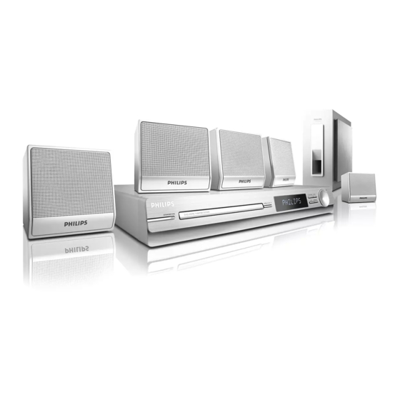
Philips HTS3000 Service Manual
Hide thumbs
Also See for HTS3000:
- User manual (47 pages) ,
- Specification sheet (2 pages) ,
- Manual (2 pages)

Related Manuals for Philips HTS3000


Summary of Contents for Philips HTS3000
- Page 1 DVD Home Theatre System HTS3000/ HTS3000/ 55/98 55/98 313 978532 750...
- Page 2 LOCATION OF PCB BOARDS TUNER PCB STANDY PCB MAIN PCB POWER PCB CONTROL PCB VOL PCB VERSION VARIATION: HTS3000 Type/Version Feature & Board in used Main PCB ( Power Output 200W) Power Voltage ( 120/230V )
- Page 3 Specifi cations AMPLIFIER FRONT AND REAR SPEAKERS Total output power System: ............Full range satellite -Home Theater Mode: ............ 200 W Impedance: ................4 Ω Frequency Response: ....... 180 Hz – 18 kHz / ±3 dB Speaker drivers: ........3” full range speaker Signal-to-Noise Ratio: ......>...
- Page 4 Measurement Setup Tuner FM Bandpass Tuner AM (MW,LW) Bandpass...
- Page 5 WAARSCHUWING WARNING Alle IC’s en vele andere halfgeleiders zijn All ICs and many other semi-conductors are gevoelig voor electrostatische ontladingen susceptible to electrostatic discharges (ESD). (ESD). Careless handling during repair can reduce life Onzorgvuldig behandelen tijdens reparatie kan drastically. de levensduur drastisch doen verminderen. When repairing, make sure that you are Zorg ervoor dat u tijdens reparatie via een connected with the same potential as the mass...
- Page 6 You will find this and more technical information • Use only lead-free solder alloy Philips SAC305 with within the “magazine”, chapter “workshop news”. order code 0622 149 00106. If lead-free solder-paste is required, please contact the manufacturer of your For additional questions please contact your local solder-equipment.
- Page 7 2 - 1 2 - 1 System , Region Code , etc. Setting Produre 1)System Reset 6)Upgrading new sofeware a) press “system “ buttom on R/C,TV show “setup“ a)open the CD Door,then insert the CD-R program disc b) select the menu using the on R/C b)close the DOOR c) go preference page to do sysytem reset...
- Page 8 2 - 2 2 - 2 REPAIR INSTRUSTRATOR Chang F901 Ok or No Check CHANG D902/903/904/908 D902/903/904/908 D909/911/912 D909/911/912 OK or No Check Repair IC901/IC902/IC903 /Q902 or output circuit...
- Page 9 3 - 1 3 - 1 Dismantling of the Main PCB DISASSEMBLY INSTRUCTIONS 2) Return the set to its upright position and remove the Tray Cover as shown in Figure 3 and close the tray manually by 1) Loosen 4 screw “ A “ on the top of main board as shown in pushing it back in.
- Page 10 3 - 2 3 - 2 Dismantling of the Control Board Dismantling of the DVD Module 1) Loosen 9 screws “ C” at the back pancle as shown in fi gure 6 1) Loosen 4 screws “E” to remove the DVD Module as shown in fi gure 8 Figure 6 Dismantling of the Power Board...
- Page 11 4 - 1 4 - 1 BLOCK DIAGRAM CONTROL PCB MAIN PCB POWER PCB...
- Page 12 4 - 2 4 - 2 WIRING DIAGRAM MAIN PCB USB PCB VOL PCB POWER PCB DVD LOADER CONTROL PCB VFD PCB...
- Page 13 5 - 1 5 - 1 FTD DISPLAY PIN ASSIGNMENT CONTROL BOARD TABLE OF CONTENTS FTD Display Pin Assignment ............. 5-1 Voltage ....................5-2 Circuit Diagram .................. 5-3 PCB Layout Top & Bottom View ............5-4...
- Page 14 5 - 2 5 - 2 VOLTAGE Q200 Pin NO Voltage -0.9 Pin NO Voltage -18.9 -25.3 -25.3 -25.3 -25.3 -16.4 23.2 Pin NO Voltage -18.6 -1836 -20.8 -25.3 -25.3 -16.5 -18.7 -16.5 -25.4 -25.4 23.2 -25.7 -23.2 -23.2 -23.2 -23.2 -23.2 -23.2 Pin NO Voltage -23.2 -23.2 -23.2 -23.2...
- Page 15 5 - 3 5 - 3 CIRCUIT DIAGRAM C200 C204 C208 C212 C216 C220 C288 D202 IC200 B1 R201 R205 R209 R213 R218 RB200A A4 TA200 C1 TA204 C1 ZD200 A2 ZD204 A3 C201 C205 C209 C213 C217 C221 C289 D203 LD200 C4 R202...
- Page 16 5 - 4 5 - 4 PCB LAYOUT - TOP VIEW C208 D202 JW12 JW18 R211 RB204 TA204 C209 D203 JW13 JW19 LD200 R213 SN200 TA205 C216 DP200 JW14 R200 R214 TA200 VR200 CN203 JW15 JW20 R201 R215 TA201 XL200 D200 JW10 JW16...
- Page 17 6 - 1 6 - 1 INTERNAL IC DIAGRAM - CO4558A SO8 MAIN BOARD TABLE OF CONTENTS Internal IC Diagram ................6-1 Circuit Diagram .................. 6-2 PCB Layout Top View ............... 6-3 PCB Layout Bottom View ..............6-4 Voltage ....................6-5 INTERNAL IC DIAGRAM - V5888S HOSP MUTE BLAS...
- Page 18 6 - 2 6 - 2 Circuit Diagram C1001 D3 C182 C441 C829 IC105 R158 R519 C1002 D3 C183 C502 C830 IC302 R159 R520 C1003 D3 C184 C504 C831 IC303 R160 R521 C1004 D3 C185 C505 C833 IC304 R162 R522 C1005 D3 C186 C506...
- Page 19 6 - 3 6 - 3 PCB Layout Top View C1111 FB125 A1 R152 C126 IC303 R325 RA101 A2 C414 Q301 R407 JK501A A4 C805 C836 Q104 R823 C165 D108 Q103 R819 C551 ZD104 B3 C567 C129 FB126 A1 R153 C323 IC304 R326...
- Page 20 6 - 4 6 - 4 PCB Layout Bottom View C193 A1 R506 A1 R526 A1 C404 A2 C427 A2 C301 A3 R124 A3 C1101 A4 C1113 A4 R1103 A4 C431 B1 C573 B1 C180 B2 C546 B2 C1007 B3 C127 B3 C856 B3 R3012 B3...
- Page 21 6 - 5 6 - 5 Voltage Q101 Q102 Q103 Q104( 2SC945P) Pin NO Pin NO Pin NO Pin NO Pin NO Voltage Voltage Voltage Voltage Voltage Pin NO Voltage Pin NO Q110 Q1101 Q1102 Q1103 Voltage Pin NO Pin NO Pin NO Pin NO Pin NO...
- Page 22 7 - 1 7 - 1 VOLTAGE Pin NO Voltage Pin NO Voltage Pin NO Voltage Pin NO Voltage POWER BOARD Q901 Q902 Q903 Q904 Pin NO Pin NO Pin NO Pin NO Voltage 30.5 31.6 Voltage -2.3 165.4 Voltage 33.3 -2.7 Voltage...
- Page 23 7 - 2 7 - 2 CIRCUIT DIAGRAM BD901 A1 C909 C917 C925 C933 C941 CN901 A4 D904 D914 IC904 Q902 R901 R909 R917 R925 R934 R943 R952 C901 C910 C918 C926 C934 C942 CN902 A4 D905 F901 L901 Q903 R902 R910 R918...
- Page 24 7 - 3 7 - 3 PCB LAYOUT - TOP VIEW BD901 C910 C921 C928 C940 C950 D901 D909 GT902 J905 J912 L905 Q905 R905 R929 TVR901 B1 C901 C911 C923 C929 C941 CN901 D902 D911 GT903 J906 J913 NTC901 B1 Q906 R908 R932...
- Page 25 7 - 4 7 - 4 PCB LAYOUT - BOTTOM VIEW C904 C914 C922 C935 C945 J901 R904 R910 R914 R921 R926 R931 R937 R945 R949 ZD901 C905 C915 C931 C937 D910 J903 R906 R911 R917 R923 R927 R934 R941 R946 R951 C908...
- Page 26 8 - 1 DVD BOARD TABLE OF CONTENTS EXPLORER VIEW ................8-2 MECHANICAL PART LIST ..............8-3...
- Page 27 8 - 2 EXPLORER VIEW...
- Page 28 8 - 3 MECHANICAL PART LIST Loc. Part No. Description BPM206009-0202 TRAY FMT020202-XXXX TRAY MOTOR HSP243174-1030 SCREW BPG206006-0001 GEAR-G POM BPG206014-0001 GEAR PULLER POM HSW258064-1040 SCREW BPG206026-0001 GEAR TRAY1 BPG206027-0001 GEAR TRAY - 2 BPG206028-0001 GEAR TRAY - 3 HSW248004-1060 SCREW BRW206004-0001 RUBB BELT...
- Page 29 9 - 1 9 - 1 Mechanical Exploded View (for /55)
- Page 30 9 - 2 9 - 2 Mechanical Exploded View (for /98)
- Page 31 Partlist HTS3000/55/98 996510003687 DVD DOOR 996510001640 DISPLAY LENS 996510001641 VOL KNOB 996510003688 FRONT CABINET 994000005305 RUBBER FOOT D14XT3.0MM W/ADV 996510001645 EJECT BUTTON 996510001646 STANDBY BUTTON 996510001258 STANDY LED LENS 996510001632 STANDBY PCB 996510001647 FUNCTION KEY 996510001634 VOL PCB 996510003685 CONTROL PCB...