Yaesu FT-902DM Instruction Manual
Hide thumbs
Also See for FT-902DM:
- Instruction manual (57 pages) ,
- Survival manual (37 pages) ,
- Instruction manual (56 pages)
Table of Contents
Advertisement
Quick Links
Advertisement
Table of Contents

Related Manuals for Yaesu FT-902DM


Summary of Contents for Yaesu FT-902DM
- Page 1 INSTRU CTION MANUAL FT -9 0 2 D M YAESU MUSEN CO., LTD. TOKYO JAPAN...
- Page 2 TABLE CONTENTS (Page) GENERAL SPECIFICATIONS CONTROLS AND SWITCHES ....... 8 REAR APRON CONNECTIONS.
-
Page 3: General Description
GENERAL DESCRIPTION The FT-902DM is precision engineered, high per The FT-902DM transceiver is entirely self-con forman�e H F transceiver of advanced design, pro tained, requiring only an antenna and power source viding all band coverage ( 160, 80, 40, 30, 20, 1 7, for operation. -
Page 4: Specifications
SPECIFICATIONS GENERA L TRANSMITTE R Frequ enc y co vera g e: Emission : L SB, USB (A3j), CW (A I), AM (A3h), FM l 60m 1. 8 - 2.0 M Hz (F3) (option FT -902SD /DE), FSK (F 1) 3.5 - 4.0 M Hz 7.0 - 7.5 M Hz PA i n put po wer :... - Page 6 SN74LS192N FE T: Va rac to r D io de: TU BE COMPLEMEN T 2SK19GR SN74LSOON 1S2209 SN74LS04N 1 S2236 2SK19TM -BL 10 12BY7A FC63 2SK34E SN74LS123N 6146B M V104 3SK40M MSM 5562 MSM 9520RS 3SK51-03 3SK59Y M M 74C90N Z en er D io de: SEMI CONDUCTO R wzoso...
-
Page 7: Controls And Switches
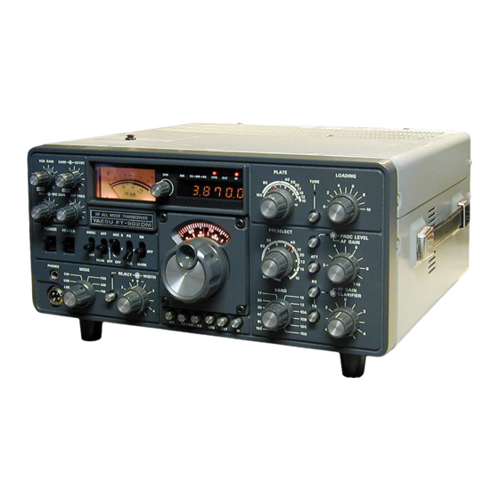
CONTROLS AND SWITCHES be certain t h a t y ou understan d t h e fun ction o f This transceiver has been specifically designed for every control b e fore operating t h e transceiver. e ase o f operation and versatility . Th e operator The various fron t p anel con trols and switches may , h owever, be un f amiliar with the operation are described in the following section . - Page 8 PRESELECT ( 1 5 ) P LATE Th i s contro l pret unes the signal circuits for both This con trol tunes the plate circuit o f the final transm i t a n d receive. Th e PRESE LECT circu i t amplifier.
- Page 9 m inimum input level from the microphone t o ( 2 4 ) P HONES 4" trigger t h e m icrophone am plifier. L ow-level back accom This is a s tandard I / phone j ack gr ound noi se w il l n o t activate the transmi tter m odatio n o f headphones .
- Page 10 REAR APRON CONNECTIONS F U S E F use h older requires 5 am p fus e for volt or Threaded lug for ground c onnection. 3 amp fuse for 220 volt operation . F or 1 2 vol t DC operation, a 2 0 amp fuse is installed in the (2 ) RF OUT...
- Page 11 the internal speaker will be disabled when p lug is insert e d . ( 16) PTT This j ack m ay be used for external actuation of the transmi t ter. As an exam p l e , a footswitch m ay be connected to this j ack to provide rem ote c on...
- Page 12 INTERCONNECTIONS FT-902DM Fl--2100Z FV-101Z/ FV-901 PING ·GNO PIN 9 (INNER CONDUCTOR) PIN 8 (OUTER CONDUCTOR) PIN 7 (INNER CONDUCTOR) PIN 8 (OUTER CONDUCTOR) EXTERNAL RECEIVER lil l MUTE PLUG .· FTV -901R FHOiOM ANTE NNA 430MHz OO TPUT RF IN...
-
Page 13: Base Station Installation
W e do not recomme nd the use o f power con fuse . When making conn ections to the car battery , nectors o ther than the ones supplie d by Yaesu . If b e absolu tely certain that t h e RED lead i s con... -
Page 15: Initial Check
3 0 d B n o tch attenuation on any interfering signal within the IF p assband. Frequ e ncy readout for the FT-902DM includes The WI D TH control v arie s the center fre both anal og and digi t al readout. The analog read... - Page 17 ( 4) R otate the PLATE con trol for a minimum SSB OPERATION m e ter reading ("dip" final a m plifier cathode curren t ) . After completion of the ab ove tuning p rocedure , Push t h e TUN E button again to return the set the MODE swi t ch to U S B or LSB as desired .
- Page 19 on . the rear panel. The FT-9 02DM is se t up for The analog display o n the transceivers p rovi d e s 1 7 0 Hz shift , and the shift frequency may b e ad easy determination of the operating frequency . justed some what by m e ans of the trimmer capaci...
- Page 20 Operation o f the memory sy stem is perhaps best Split-frequency con trol may b e ob tained with the described by the use o f some example s : m e m ory sy stem or the FV -9 0 1 DM synthesized scan ning VFO.
- Page 21 �x RX ) 8989 k H z US B . C W( R X ) i..5 8 ; rx R X ) F S K! R X J 8986 k H z AM . :MARKER - -=--� -=-+ - � F S K ( TX ) 8 9 88 .
- Page 22 C I R C U I T D E S C R I P T I O N This transceiver utilizes PLL (Phase Locked Loop ) RF U NIT (PB-2 1 54 ) circuitry. The receiver is a single-conversion type T h e incoming signal is amplifie d by t h e R F ampli...
-
Page 23: Fi Lter Unit
FI LTER UNIT ( P B- 1 9 9 5 ) IF U NIT ( P B - 1 704C ) T h e I F signal fro m p i n is fe d t o t h e ga t e o f t h e The I F signal re c e i v e d a t p i n o f the F I LT E R I F fi rs t m i x e r , Q4 0 ! ( 3 S K 5 1 - 0 3 ) . - Page 24 The output from the I F second mixer is fe d The RF GAIN c on trol on the fron t p anel varies th rough a mono I i thic fil ter 402 to the two-stage the AGC vol tage leve l , providing manual con trol IF ampl ifier consisting of Q 403 an d Q404 (both of the gain of the RF and IF s tage s .
- Page 26 CARRIER UNIT ( P B -1706A) The carrier oscillator Q702 (2SK 19G R ) is followed b y a buffer amplifier Q703 ( 2SC181 SY) . It oscil l a tes at one of the following f r equencies, depend ing on the mode of operation : 8 9 8 9 kHz with X 7 0 2 ;...
- Page 27 AF UNIT ( PB- 1 705A ) The audio signal from the AM detector is ampli fied by Q5 0 7 ( 2 SC 7312TM) and fed to the first audio amplifier Q 5 0 1 (2SC 7 32TIM) . On S S B , CW , F M , and F S K , the audio signal is directly fed to Q 5 0 1 from pin 1 5 .
- Page 28 The drain of Q2 1 2 is d irectly connected to the NB UNIT (PB- 1 994 ) base of Q 3 0 3 in th e F I LTER UN I T . ( 2SC I 8 1 SY) As t h e drain voltage o f Q 2 1 2 d rops, the base p ortion o f t h e 8 9 8 7 .
- Page 29 TRAN S MIT CIRCUIT between the collector and emitter of Q 2 0 7 ( 2 SC 181 S Y ) , thus changin g the in put sign al level t o the filter. S S B The CW, FSK, AM , and F M signals pass through and are fed to The ou tput from t h e M IC j ack J is fed through...
- Page 30 Keyer speed is controlled by V R 2 b on the fron t provide s adjustment o f the dot panel. V R2 7 0 1 space symme try , while adjusts th e keying VR2 7 0 2 In th e CW , AM , and FSK modes, carrier oscillator Q 7 0 2...
- Page 32 a n active low pass fil te r to eliminate harm onics The VOX GAIN con trol · Y R , the fron t pane l c aused b y the clipping. V R 9 0 2 de termines t h e p rovides adju stme nt fo r relay sensi tivity , a nd m ax i m u m deviation .
- Page 34 prior to being supplied to a phase d e tector Q , 1 0 7 portion o f the Q , 2 0 9 output is rectified by ( MC4044P ) ; here the phase of the signal is com an d ( b o th 1 N60) ;...
- Page 36 COUNTER UNIT ( PB-2086A-3 4 3 0 /PB-2098) The output from the LSI is fed to the display . Th e output from pins 2 4 through i s delivered t o The local oscillator signal is applied to Large- Scale segment d rivers Q 3 0 1 3 -Q 3 0 1 9 ( 2SA9 5 2 L)
- Page 37 2 S A 4 9 6 - Y _ _ _ _ _ _ _ _ _ _ _ _ 0 0 1 F IN � ��� � � r � I " � � 0 2 0 JJ PA 54 H L O I z'"...
- Page 40 PB- 1 71 2 A RECT B UNIT - - - - - - - - - Dl402 10DIO D i401 IODIO Cl502 100.u 500 w v Rl403 4mK Rl404 470K L - - CAPACI TOR UN I T r - - - - - - - - - - - - - - - - - - - - - - - - - - - - - , '°...
- Page 41 AM/CW FILTER INSTALLATION Remove the top cover. Locate and remove PB- 9[9i 5 (FI LTER UNIT). Referring to Fig. 1 , l ocate jump ers A and B on the prin ted b oard. If the AM filter is to be i nstalled, the jumper marked A . must b e removed, an d for C W filter installation the j umper marked B mu st b e removed.
- Page 42 FM UNI T I N STALLATION FOR FT-902DE/SD R E A R The FM Unit operation fo r t h e FT-9 02D E and m o dels can be installed in a matter o f minutes. R estra i n i n g Re move the top cover of the transceiver, and re...
- Page 43 DC-DC CONVERTER INSTALLATION The optional D C-DC converter is easy to install in ( 4) B e fore connecting the D C power cable to the transceiver, check the automobile voltage a matter of minutes. Please follow the instructions c are fully , in order t o m ake the proper connections . regulator level with the engine running ( ba t...
-
Page 44: Bottom View
KEYER/MEMO RY UNIT INSTALLATION Remove the small cover from the b ottom o f the 6 5 30060 I ZG transceiver as shown in Fig. 1 . Install the UNIT u sing the mounting MEMORY screws supplied . Connect the 6-pin connector to the socket on the m ain chassis as shown. - Page 45 A n t e n n a F u s e DC - D C C o n v e r t e r U n i t ( FH 1 ) D r i v e B o a rd ( P B - J 7 1 4 ) V 1601 R F U n i t...
-
Page 46: M Aint Enance And Align Ment
RF probe good t o 4 0 MHz. ( 3 ) Dummy Load : Yaesu model YP- 1 5 0 o r equiv alent , wit h 50 Ohm n on-reactive load imped ance rated to 1 5 0 watts average p ower. - Page 47 VOX ADJUSTMENT m atched an tenna or dummy load . Turn the M I C G A I N control fully counterclockwise to rem ove Tune in a sign al and adjust the AF GAIN con trol all audi o input f r om the modulator stage . for a n ormal listening leve l .
- Page 48 V R 7 0 1 V R 203 V R 202 V R 2 0 1 T 2 0 7 Q 7 0 1 X 7 o 3 Q 7 0 3 X 7 D 2 X r n 1 X F2 0 1 Q207 V R , 0 2...
-
Page 49: Voltage Regulator Adjustment
1 1 . KEY E R ADJ USTMENT V R2 7 0 2 con trols the d ot-to-space ratio for the buil t-in e l e c tronic key er ; this is normally set to a t the factory . VR 2 7 0 1 adjusts the symme try b etween d o ts and d ashes. - Page 50 1 5 . POWER OUTPUT METER ADJUSTMENT ( 2 ) Locate TC0 1 , t h e neutralization variable capacitor shaft , on the i n side wall o f the V R 7 , l ocated on the transceiver rear panel adj a final amplifier comp artme n t .
- Page 51 ALIGNM ENT TRANSMITTER MIXER/ ( 1 1 ) Now you are ready t o align the other bands . D RIVER AND RECEIVER F RONT END STAGE Set the B AND switch to 1 5 , set th e m ain tuning dial for a reading of 2 1 .000 MHz, and ( 1 ) Connect a dummy load/wattme ter to the...
- Page 53 C r y s t a l unit ( P B - 1 7 1 1 ) Select Switch Boa r d ( PB · \ 7 1 8 ) & > > M e m o ry u n i t ( P B - 1 7 87 ) Q g 1 1 Qg 1 0 Qgo3...
- Page 54 YA E SU 8103 - A...