Table of Contents
Advertisement
Quick Links
SAFETY PRECAUTION OF MD SECTION FOR SERVICE MANUAL .............................................................................. 2
SAFETY PRECAUTION OF CD SECTION FOR SERVICE MANUAL .............................................................................. 3
VOLTAGE SELECTION ..................................................................................................................................................... 3
AC POWER SUPPLY CORD AND AC PLUG ADAPTOR ................................................................................................. 3
SPECIFICATIONS ............................................................................................................................................................. 4
NAMES OF PARTS ........................................................................................................................................................... 5
OPERATION MANUAL ...................................................................................................................................................... 7
DISASSEMBLY ................................................................................................................................................................ 10
REMOVING AND REINSTALLING THE MAIN PARTS ................................................................................................... 13
DESCRIPTION OF CIRCUIT FOR 1-BIT AMP. UNIT ..................................................................................................... 15
TO CHECK AND CANCEL PROTECT CIRCUIT DETECTION LINE .............................................................................. 16
TEST MODE .................................................................................................................................................................... 17
ADJUSTMENT ................................................................................................................................................................. 22
ERROR MESSAGE LIST ................................................................................................................................................. 31
EEPROM WRITING PROCEDURE ................................................................................................................................. 32
NOTES ON SCHEMATIC DIAGRAM .............................................................................................................................. 35
TYPES OF TRANSISTOR AND LED ............................................................................................................................... 35
BLOCK DIAGRAM ........................................................................................................................................................... 36
SCHEMATIC DIAGRAM .................................................................................................................................................. 40
WIRING SIDE OF P.W.BOARD ....................................................................................................................................... 54
WAVEFORMS OF 1 BIT AMP. CIRCUIT ......................................................................................................................... 67
WAVEFORMS OF MD CIRCUIT ..................................................................................................................................... 68
WAVEFORMS OF CD CIRCUIT ...................................................................................................................................... 70
TROUBLESHOOTING ..................................................................................................................................................... 72
FUNCTION TABLE OF IC ................................................................................................................................................ 81
FL DISPLAY ...................................................................................................................................................................... 98
PARTS GUIDE/EXPLODED VIEW
SERVICE MANUAL
MODEL
CONTENTS
SHARP CORPORATION
1-BIT DIGITAL AUDIO SYSTEM
SD-CX1W(BL)
SD-CX1W(GR)
SD-CX1W 1-Bit Digital Audio System consisting of SD-CX1W (main
unit) and CP-CX1W (speaker system).
• In the interests of user-safety the set should be restored to its original
condition and only parts identical to those specified should be used.
This document has been published to be used
for after sales service only.
The contents are subject to change without notice.
SD-CX1W
No. S3117SDCX1WBL
Page
Advertisement
Table of Contents

Related Manuals for Sharp SD-CX1W(BL)


Summary of Contents for Sharp SD-CX1W(BL)
-
Page 1: Table Of Contents
WAVEFORMS OF CD CIRCUIT ............................70 TROUBLESHOOTING ..............................72 FUNCTION TABLE OF IC ..............................81 FL DISPLAY ..................................98 PARTS GUIDE/EXPLODED VIEW This document has been published to be used SHARP CORPORATION for after sales service only. The contents are subject to change without notice. -
Page 2: Safety Precaution Of Md Section For Service Manual
SD-CX1W SAFETY PRECAUTION OF MD SECTION FOR SERVICE MANUAL WARNINGS The AEL (Accessible Emisson Level) of the laser power output is less than class 1 but the laser component is capable of emitting radiation exceeding the limit for Class 1. Therefore it is important that the following precautions are observer during servicing to protect your eyes against exposure to the laser beam. -
Page 3: Safety Precaution Of Cd Section For Service Manual
SD-CX1W SAFETY PRECAUTION OF CD SECTION FOR SERVICE MANUAL WARNINGS Precaution to be taken when replacing and servicing the Laser Pickup. The AEL (Accessible Emission Level) of Laser Power Output for this model is specified to be lower than Class 1 Requirements. However, the following precautions must be observed during servicing to protect your eyes against exposure to the Laser beam. -
Page 4: Specifications
SD-CX1W FOR A COMPLETE DESCRIPTION OF THE OPERATION OF THIS UNIT, PLEASE REFER TO THE OPERATION MANUAL. SPECIFICATIONS SD-CX1W General Power source AC 110/127/220/230-240 V, 50/60 Hz Power consumption 42 W Dimensions Width: 330 mm (13") Height: 208 mm (8-3/16") Depht : 187 mm (7-3/8") Weight 5.3 kg (11.7 lbs.) -
Page 5: Names Of Parts
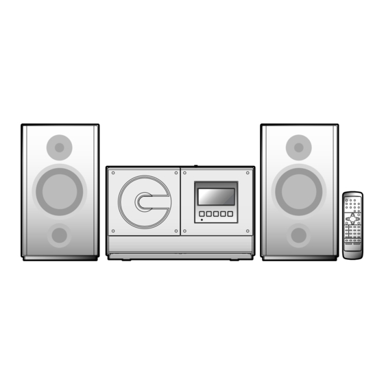
SD-CX1W NAMES OF PARTS SD-CX1W Front panel 1. CD Cover 2. CD Cover Open/Close Button 3. Remote Sensor 4. Function Indicator 5. Timer Indicator 6. On/Stand-by Button 7. MD Compartment 8. MD Eject Button 9. MD Record Mode Button 10.CD/MD Play Mode Select Button 11.MD Stop Button 12.MD Play/Pause Button 13.CD Stop Button... - Page 6 SD-CX1W Remote control 1. Remote Control Transmitter 2. CD/MD Play Mode Select Button 3. MD Record Mode Button 4. On/Stand-by Button 5. MD Record Button 6. Top Position Button 7. Track Edit Button 8. Sound Synchronise Record Button 9. Volume Up or Down Button 10.CD/MD Fast Reverse, Tuning Down Button 11.Extra Bass Button 12.CD/MD Programme Button...
-
Page 7: Operation Manual
SD-CX1W OPERATION MANUAL Setting the Clock Press the REC LEVEL/CURSOR button to adjust the date, and then press the ENTER button. Press the REC LEVEL/CURSOR button to adjust the hour, and then press the ENTER button. Press the REC LEVEL/CURSOR or button to adjust the minutes, In this example, the clock is set for 9:30 15. - Page 8 SD-CX1W Setting the FM/AM span selector The International Telecommunication Union (ITU) has established that member coun- tries should maintain either a 100 kHz or a 50 kHz interval between broadcasting fre- quencies of FM stations and 10 kHz or 9 kHz for AM station. The illustration shows the 50/9 kHz zones (regions 1 and 3), and the 100/10 kHz zone (region 2).
- Page 9 SD-CX1W Error Messages When an error message is displayed, proceed as follows: Error messages Meaning Remedy Error messages Meaning Remedy BLANK MD Nothing is recorded. (Neither Replace it with another disc. MD NO DISC A MiniDisc has not been load- Load a MiniDisc.
-
Page 10: Disassembly
SD-CX1W DISASSEMBLY Caution on Disassembly SD-CX1W Follow the below-mentioned notes when disassembling the unit and reassembling it, to keep it safe and ensure Front Panel excellent performance: 1. Take compact disc and mini disc out of the unit. (A1)x3 ø3x12mm 2. - Page 11 SD-CX1W (M1)x1 (E1)x1 (M3)x2 ø3x8mm ø3x6mm (E2)x1 (E2)x1 LED PWB (E3)x1 (M1)x2 (N2)x1 Eject ø3x8mm (N1)x4 (F2)x1 Main Trans Power (M1)x8 ø3x8mm Headphons Tuner Front Panel Sub Trans (M2)x1 Display PWB (F1)x1 Main PWB ø3x10mm Figure 11-4 MD Unit (P9)x2 Figure 11-1 ø3x8mm (G2)x1...
- Page 12 SD-CX1W SD-CX1W (MD MECHANISM UNIT) CP-CX1W STEP REMOVAL PROCEDURE FIGURE STEP REMOVAL PROCEDURE FIGURE Rear Cabinet 1. Screw ....(A1) x6 12-2 MD Mechanism 1. Screw ....(Q1) x4 12-1 holder (Left/Right) Tweeter 1. Screw ....(B1) x4 12-3 Shield Cover 1.
-
Page 13: Removing And Reinstalling The Main Parts
SD-CX1W REMOVING AND REINSTALLING THE MAIN PARTS MD MECHANISM SECTION (A1)x1 For details about the procedure to remove the MD mechanism ø1.7x5mm from the main unit, refer to the Disassembly Procedure, Steps 1-8 and 15-18 in the main unit and also the MD section. (Referring to pages 10 and 12.) Magnetic Head Caution:... - Page 14 SD-CX1W How to remove the MD spindle motor (D1)x3 ø1.4x3mm (See Fig. 14-1) 1. Remove the screws (D1) x 3 pcs., and remove the MD MD Spindle Motor spindle motor. Caution: Be careful so that the gear is not damaged. (The damaged gear emits noise during searching.) Figure 14-1 CD MECHANISM SECTION...
-
Page 15: Description Of Circuit For 1-Bit Amp. Unit
SD-CX1W DESCRIPTION OF CIRCUIT FOR 1-BIT AMP. UNIT (SEE THE SCHEMATIC DIAGRAMS ON PAGES 50 AND 51.) Input Low-pass filter circuit Signals over certain level input from BIA106 are sliced into 1-bit signals switched at FET are converted into analog waveforms by RA173 (RA174), DA126, and DA127 (DA128, signals via the low-pass filter consisting of LA100 (LA102, DA129). -
Page 16: To Check And Cancel Protect Circuit Detection Line
SD-CX1W TO CHECK AND CANCEL PROTECT CIRCUIT DETECTION LINE 1. After power supply, the microcomputer (ICD01) built in this 4. Abnormalities of cooling fan motor and its driving model consecutively monitors the following errors 1 to 4. If circuit (stop, etc.) any error occurs, 'Er_AP00' is displayed and all power Turn on the unit to visually inspect the cooling fan motor till the protective operation starts. -
Page 17: Test Mode
SD-CX1W 1-BIT AMP. SECTION Wiring diagram of the 1-bit Amp. unit After the wires from the 1-bit amp PWB are wound around the cores as shown in Fig. 17, secure them to the chassis of amp unit with nylon bands (4 pcs). Nylon Band Core Nylon Band... - Page 18 SD-CX1W Test mode Version display SKIP-DWN With SKIP-UP button Version display to CD-PLAY SKIP-UP SKIP-DWN Version display to MD-PLAY SKIP-DWN SKIP-UP Version display to ERASE SKIP-DWN SKIP-UP Version display to MD-REC SKIP-DWN SKIP-UP Version display to AUX(DEMO) SKIP-DWN SKIP-UP Version display to CD-STOP SKIP-DWN SKIP-UP...
- Page 19 SD-CX1W 1. CD test Outline: Readout of the set value after automatic adjustment (for judging difference from initial value). Forced operation of pickup (Inner/Outer circumference feed). During the PLAY mode, the number of errors accumulated for 10 seconds (750 frames) is displayed. Basic CD operation by CD-PLAY button During the TEST mode, the display is turned on and the following buttons become effective.
- Page 20 SD-CX1W Double-speed mode Press the MD-REC button in the stop mode to switch to the double/constant-speed mode cyclically. During the double-speed mode, a flag mark lights up. CD TEST N:NORMAL SPEED H:HIGH SPEED STEP NO Display Time Display TNO Display [CD] Flashing STEP NO Display Time Display...
- Page 21 SD-CX1W 7. KEY test Outline: To check if KEY data are input to the microcomputer accurately. Operation All lights of segments on FL go off while the keys are not effective. Segments corresponding to the keys are lit up as shown below. The power button is an exception;...
-
Page 22: Adjustment
SD-CX1W ADJUSTMENT • Setting the Test Mode TUNER SECTION When setting the tuner test mode, the frequencies are initialized fL: Low-range frequency in the memory as shown in Table 22. Refer to the microcomputer fH: High-range frequency test mode function on pages 17 and 21. If the initialization is executed, the frequencies registered by •... - Page 23 SD-CX1W CD SECTION Since this CD system has the built-in automatic adjustment function, readjustment is not necessary when replacing the pickup. Therefore, any combinations of PWB and pickup can be made. Since automatic adjustment is executed every time the disc is changed, each disc can be played in the most appropriate condition. MD SECTION Enter the test mode, adjust or set as shown in the following table according to the repair operations.
- Page 24 SD-CX1W 1. Preparation for adjustment Test disc Type Test disc Part No. High reflection disc TGYS1 (SONY) [for Playback] RRCDT0101AFZZ Low reflection disc MiniDisc for checking the recording operation –––––––––––– (commercially available MD) Head Adjusting transparent RRCDT0103AFZZ Low reflection disc Pre-adjustment disc [TEAC Test MD] 88GMMD-213AS or 88GMMD-318 2.
- Page 25 SD-CX1W 1. EJECT mode Step No. Setting Method Remarks Display Step 1 Test mode EJECT state [ _ _ E J E C T _ _ _ ] Step 2 Press the CD STOP button. Playback power output state [ p p w _ _ _ _ _ _ _ ] Step 3 Press the CD STOP button.
- Page 26 SD-CX1W 4. AUTO AFB adjustment mode Step No. Setting Method Remarks Display Step 1 Test mode STOP state [ t s m Step 2 Press the CD PLAY button two times. AUTO AFB adjustment menu [ _ A U T _ A F B _ _ ] Step 3 Press once the MD PLAY button.
- Page 27 SD-CX1W c) Tracking setting Step No. Setting Method Display Step 1 Test mode STOP state [ t s m Step 2 Press the CD PLAY button eight times. [ E E P R O M_ S E T ] Step 3 Press the MD PLAY button.
- Page 28 SD-CX1W e) TEMP setting Setting Method Display Step No. Step 1 EJECT state (or state without mechanism) [ _ _ E J E C T _ _ _ ] Step 2 Press the TUNER (BAND) button. [ T E M P_ •...
- Page 29 SD-CX1W h) REC bit setting Setting Method Display Step No. Step 1 Test mode STOP state [ t s m Step 2 Press the CD PLAY button eight times. [ E E P R O M_ S E T ] Step 3 Press the MD PLAY button.
- Page 30 SD-CX1W 1. Adjustment Load a high-reflective TGYS1 test disc. Note: Adjust the position of the lead-in switch between FF85 to (A1)x1 FFD2. 1. Loosen the screw (A1) x 1 pc., fixing the mechanism switch PWB. 2. Retighten the screw while pushing the PWB in the direction of arrow A if the switch position is at FF85 or lower, or in the direction of arrow B if it is at FFD2 or higher, and measure its position again.
-
Page 31: Error Message List
SD-CX1W ERROR MESSAGE LIST MD error messages Error Display Error Message Remarks Can't REC • Errors occurred 10 times continuously in the REC-PLAY • Check for scratch, dust, fingerprints, or black spots on mode. the disc. Check that the disc is not eccentric or largely •... -
Page 32: Eeprom Writing Procedure
SD-CX1W The details description of mechanism error HINF Error Display Error Message (93 Pin of IC1401) E r - M D 1 Ejection is not completed. EJECT complete position < 1.0 V E r - M D 2 Head-up is not completed. LOAD/EJECT halfway position >... - Page 33 SD-CX1W Tracking setting Control setting Item indication Setting Item indication Setting C O N T R L 1 C O N T R L 2 T G 2 A D J T T M T F 0 H D E Q A D T F 1 T F 2 L D E Q A D...
- Page 34 SD-CX1W – 34 –...
-
Page 35: Notes On Schematic Diagram
SD-CX1W NOTES ON SCHEMATIC DIAGRAM • Resistor: • Schematic diagram and Wiring Side of P.W.Board for this To differentiate the units of resistors, such symbol as K and model are subject to change for improvement without prior M are used: the symbol K means 1000 ohm and the symbol notice. -
Page 36: Block Diagram
SD-CX1W FE301 FM IF TP302 CF302 FM FRONTEND 75ohms AM IF CF351 FM IF SO301B T351 CF352 X351 ANTENNA AM IF 456kHz TERMINALS FM IF IC303 MUTE LA1832 LELEL FM IF DET./FM MPX./AM IF AM OSC VR351 10K(B) PHASE VOLTAGE REGURATOR TP301 IC302 LC72131... - Page 37 SD-CX1W L-CH ANALOG IN L-CH L-CH_IN L-CH TO MAIN SECTION R-CH ANALOG IN R-CH R-CH R-CH_IN ICA101~ICA104 GATE DRIVER DA126 DA129 TO DISPLAY HIP2100 SECTION TEST +11V R-CH_OUT(+) GNDX DA128 DA127 OUTPUT FET ICA100 NFR1(+) QA100 1 BIT AD NFR2(–) SLA5001 CXA100 VRA100...
- Page 38 SD-CX1W SW601 FLD01 SPAN SELECTOR FL DISPLAY 50/9 57 59 100/10 8.3886MHz XLD01 HEADPHONES +B12 +B13 –VP MAIN SECTION JHP01 HEADPHONES 10 0 SPAN MD_LOADSW MD SECTION H.P_SW MD_ST CD_OP/CL_SENS MD_SERCH DR_OP_IN MD_RESET CD SECTION DR_CL_IN MD_D_STB_ TIMER_LED MD_DSCK ICD01 MD_KDATA LEDD02 MD_DATA_...
- Page 39 SD-CX1W TO MAIN UNIT TO CD UNIT 1 2 3 4 5 6 7 8 9 10 11 12 13 14 15 16 17 18 19 20 21 22 23 24 25 26 27 28 CN1501 1 2 3 4 CN1502 MECHANISM +4.75~5.25V...
-
Page 40: Schematic Diagram
SD-CX1W MAIN PWB-A1 CU34 RU30 ZDU02 100P(CH) DZ10BSB ICU01 CU33 100/10 (OS-CON) AUDIO PROCESSOR RU32 CU32 100/16 LC75341M CU35 RU31 CU31 0.022 100P(CH) RU33 220(1/2W) 4.8V RU34 220(1/2W) CU36 8.4V DU01 100P(CH) CU45 (OS-CON) DS1SS133 100/10 4.2V CS02 CU30 RU12 CU17 4.2V 0.082(ML) - Page 41 SD-CX1W RU19 L-CH CU21 RU17 470P JTU01 AUX INPUT RU18 CU22 470P R-CH RU20 ICP01 PRE AMP. CP10 CP04 CP02 RP02 RS06 RS04 NJM4565M 2.2/50 22P(CH) 2.2/50 4.7K RS12 RS26 CS08 MUTING RS24 RS10 0.22/50 CU43 CS06 100K QP02 RP04 100K CP06 0.001...
- Page 42 SD-CX1W TUNER PWB-A2 AM TRACKING fL C331 0.047 C330 15P(UJ) C338 C324 C323 T302 C332 0.0022 0.022 0.022 0.47/50 AM ANTENNA L353 2.8V(1.3V) VD301 C339 SVC348S AM BAND 100P(CH) COVERAGE BI303 C335 330P C337 C334 R323 T306 0.022 AM OSC. (UJ) R336 2.2V...
- Page 43 SD-CX1W TP302 R364 R363 4.7K 4.7K C372 R362 1/50 R350 2.7K C367 1/50 X351 R361 C371 456kHz 1/50 IC303 LA1832 FM IF DET./ IC303 FM MPX./AM IF LA1832 4 5 6 3.9V 2.1V (1.3V) R352 T351 5.1V C358 1/50 R353 R355 3.3K R354...
- Page 44 SD-CX1W CD PWB-A3 8 7 6 5 IC101 – OPE AMP. KIA358P – 1 2 3 4 C101 CNS102 R103 BI102 TO POWER PWB 2.2K CNP102 R101 C102 R102 100K P48 1-D CD PICKUP UNIT R107 A_3R3V A 3.3V GH6C605B3A1 0.022 SERVO PRE AMP.
- Page 45 SD-CX1W CD SIGNAL R108 R104 FROM MAIN 7 6 5 D_OUT CNSU01 – 14 13 12 11 10 9 8 P41 12-G – 2 3 4 R111 CNP8 C103 DATA 1 2 3 4 5 6 7 DATA FROM MD CDGND1 100mA CW1502B...
- Page 46 SD-CX1W DISPLAY PWB-B1 FLD01 FL DISPLAY 10 11 12 13 14 15 16 17 18 19 20 21 22 23 24 25 26 27 28 29 30 31 32 33 34 35 36 37 38 39 40 41 42 43 44 70 69 68 67 66 65 64 63 62 61 RE02 SEG15 -25V...
- Page 47 SD-CX1W FWD03 GND_D BUS3 BUS2 BUS1 BUS0 41 42 43 44 45 46 47 48 49 50 51 52 53 54 55 56 57 58 59 BUCK PU_IN TO CD PWB DR_OP_IN QD01 CNPD1 DR_CL_IN KRC107 M P45 12-C CD_RESET DR_M+ DR_M- CD_FUNC...
- Page 48 SD-CX1W CV92 330P FWM01 GND_MD CV97 CV99 FROM 0.001(ML) 0.001(ML) GND_MD 1 BIT AMP. L– +12V(A) CV98 +5V_MD_D 0.001(ML) CNSA110 R– P51 12-D GND_D +6V(A_MD) Q803 R823 GND_A KTC3199 GR 100K 0.7V GND_A D821 R822 –12V_A –B RV85 DS1SS133 R824 4.7K (1W) SUR_ON/OFF...
- Page 49 SD-CX1W L-CH L– SOV99 R– SPEAKER TERMINALS R-CH RV73 RV63 RV61 180K RLV99 RV64 RV62 RELAY RV82 RV78 CV80 0.0022 RV67 4.6V ICV98 DV93 KIA4558P -0.3V DS1SS133 RV83 RV79 4.6V OPE AMP. DV92 ICV98 -9.8V DS1SS133 CV81 4.7V -11.2V 0.022 QV87,QV88,QV90,QV91,QV93,QV94: FAN CONTROL 10.9V...
- Page 50 SD-CX1W RA176 RA174 2.2K 8.2K R-CH ANALOG IN R-CH –B R-CH RA173 8.2K ANALOG IN L-CH L-CH L-CH CA165 100/10 RA101 RA100 1.2V 2.2K 2.2K CA164 DA126 DA129 100/10 1SS361 1SS361 RA178 CA196 1.2V 47/25 2.5V DA127 DA128 CA182 RA180 TEST 1SS361 1SS361...
- Page 51 SD-CX1W CNSA106 R-CH_IN TO MAIN PWB LA127 LA124 AGND CNPP01 L-CH_IN P41 12-B CA211 CA214 0.001 LFA01 6.75µH CORA02 CNSA112 CA196 A+5V 47/25 AGND_AD TO POWER PWB D+5V CNP802 DGND_AD CA197 P48 3-C 47/25 RESET LFA02 6.75µH RA153 FM SIGNAL 1 BIT AMP.
- Page 52 SD-CX1W MD MAIN PWB-E TP1131 C1117 TP1116 0.7V 1.1V 1.3V 1.3V 1.8V 1.7V 2.6V 1.3V 1234 VCC1 EFMAGC SYRS 0.7V 1.3V 1.3V TP1201 EFMMON C1123 C1201 0.7V 1.3V AVCC1 EFMO-I EFMO-I ADAGI EFMI C1121 C1261 AGND1 0.7V 0.22 ADAGC 220P(CH) AVCC2 R1266 C1211...
- Page 53 SD-CX1W MD SIGNAL CD SIGNAL PLAYBACK SIGNAL 1.6V RECORD SIGNAL TP1212 SYRS 1.6V EFMMON DADATA DADATA AVCC1 2.6V ADDATA 1.3V EFMI ADDATA 1.6V R1211 DFCK AGND1 DFCK 1.6V BCLK AVCC2 2.6V BCLK 1.6V LRCK VREF 1.3V LRCK C1206 1.3V DGND PLLBVC 1.3V R1212...
-
Page 54: Wiring Side Of P.w.board
SD-CX1W MAIN PWB-A1 (TOP VIEW) COLOR TABLE BROWN R D ( R ) ORANGE YELLOW GREEN BLUE VIOLET GRAY W H ( W ) WHITE BLACK PINK Figure 54 WIRING SIDE OF P.W.BOARD (1/13) – 54 –... - Page 55 SD-CX1W FROM 1 BIT AMP. PWB P63 7-G MAIN PWB-A1 (BOTTOM VIEW) CNSA106 RS19 QS01 RP27 CNPP01 1 2 3 1 2 3 RS05 CP09 RS11 RP01 RP03 CS09 CS05 RU20 R-CH CP05 RS03 RS13 RP06 RP05 RS01 RS09 ICP01 RS18 JTU01 ICS01...
- Page 56 SD-CX1W TUNER PWB-A2 (TOP VIEW) Figure 56 WIRING SIDE OF P.W.BOARD (3/13) – 56 –...
- Page 57 SD-CX1W SO301B ANTENNA TERMINALS COLOR TABLE BROWN RD(R) ORANGE BI303 YELLOW C338 GREEN T302 D302 BLUE VIOLET D301 GRAY C394 WH(W) WHITE C332 C330 R369 C331 C393 D304 BLACK VD301 C339 D303 X352 C335 R336 PINK C301 C334 R381 R380 C397 TP301 R374...
- Page 58 SD-CX1W CD PWB-A3 (TOP VIEW) PICKUP UNIT COLOR TABLE BROWN R D ( R ) ORANGE YELLOW GREEN BLUE VIOLET GRAY W H ( W ) WHITE 7 6 5 4 3 2 1 BLACK 8 7 6 5 4 3 2 1 PINK Figure 58 WIRING SIDE OF P.W.BOARD (5/13) –...
- Page 59 SD-CX1W FROM MD PWB FROM MAIN PWB TO POWER PWB CNP102 P60 1-G P64 6-C P55 12-E CW1502B CNSU01 CD PWB-A3 CNS102 (BOTTOM VIEW) E C B BI102 CNP8 CNP7 FWD03 CNPD1 R108 ZD101 R102 R107 1 2 3 4 R106 C101 IC101...
- Page 60 SD-CX1W BI800 POWER PWB-B2 CNS800 D804 C800 D803 C801 C809 C807 D802 C810 D801 D805 D806 D823 IC804 C833 C806 D808 BI02 D807 C831 C813 C832 C828 IC803 ZD801 C826 ZD800 R804 C827 R801 C824 R803 C818 R800 D815 IC802 B C E Q800 D814...
- Page 61 SD-CX1W MAIN TRANS PWB-B3 COLOR TABLE CN902 BROWN RD(R) ORANGE YELLOW GREEN BLUE F801 VIOLET T5A L 250V GRAY WH(W) WHITE BLACK PINK T901 MAIN POWER TRANSFORMER CNS900 CNS901 BI901 T.F. AC POWER SUPPLY CORD AC 110/127/220/230-240 V, 50/60 Hz SUB TRANS PWB-B4 T900 L900...
- Page 62 SD-CX1W LA100 LA104 ICA101 ICA102 ICA103 ICA104 CA121 CA128 CA118 CA131 RA170 CA126 ICA110 RA120 CA115 DA107 CA112 DA106 CA113 RA119 CA114 CA104 RA108 1 BIT AMP. PWB-C (TOP VIEW) • The numbers are waveform numbers shown in page 67. Figure 62 WIRING SIDE OF P.W.BOARD (9/13) –...
- Page 63 SD-CX1W TO POWER PWB TO POWER PWB P60 1-E P60 6-E CNP801 CNPV99 CNSA111 CNSA110 CORA03 CORA01 LFA04 LFA05 BIA111 BIA110 RA341 LFA03 LFA06 CA224 RA340 CA223 ICA105 CA150 QA103 DA131 CA179 QA102 RA130 CA192 LA130 LA132 DA114 DA117 DA113 QA100 QA101 9 8 7 6 5 4 3 2 1...
- Page 64 SD-CX1W COLOR TABLE BROWN MAGNETIC HEAD(34) R D ( R ) P55 11-H (RECORD) ORANGE CNPU04 TO MAIN PWB YELLOW GREEN BLUE VIOLET CW1501 GRAY W H ( W ) WHITE BLACK PINK 1 2 3 4 TP1543 CN1300 TP1702 CN1501 TP1301 TP1524...
- Page 65 SD-CX1W MD LOADING M903 MD LOADING MOTOR PWB-F2 MOTOR TP1971 SW1934 PLAY TP1972 R1932 TP1973 TP1975 SW1933 SW1931 RECORD DISC MEDIA CN1931 TP1974 SW1930 SW1932 WRITE PRO LOADING IC1702 C1707 C1509 R1704 C1606 L1552 Q1700 Q1702 R1705 R1516 C1304 R1513 R1561 L1551 R1511...
- Page 66 SD-CX1W HEADPHONES PWB-B6 CD EJECT PWB-B5 COLOR TABLE BROWN R D ( R ) SWD07 CD EJECT ORANGE JHP01 YELLOW HEADPHONES CD56 BID03 GREEN DD07 BLUE DD08 LD04 (251) VIOLET BID02 GRAY TO POWER PWB W H ( W ) WHITE TO CD PWB P60 1-H...
-
Page 67: Waveforms Of 1 Bit Amp. Circuit
SD-CX1W WAVEFORMS OF 1-BIT AMP. CIRCUIT 2.00V/div 2.00V/div 2.00V/div 2.00V/div AD IC Output LEVEL SHIFT OUT + Side POWER SUPPLY - Side 500ns/div 194.545465µs 520mV 500ns/div 194.545465µs -12.47V Amplitude Waveform after level shift from 0 to 5 V On the reference side, 5 V amplitude is observed at + 2 V (negative supply voltage), corresponding to VINH and VINL of gate driver during 9 V operation. -
Page 68: Waveforms Of Md Circuit
SD-CX1W WAVEFORMS OF MD CIRCUIT POWER ON TOC READ (Low reflection disc) TP1122 (F+) TP1518 (RESET) TP1207 (TEMON) TP1603 TP1800 (3.2V) (SP+) TP1602 TP1511 (SP-) (PCONT0) TOC READ (High reflection disc) TOC READ (Low reflection disc) TP1122 TP1122 (F+) (F+) TP1207 TP1212 (TEMON) - Page 69 SD-CX1W PLAY (Low reflection disc) TP1201 (EFMMON) TP1300 (REC HEAD) TP1207 (TEMON) TP1302 (EFMO) TP1121 (T+) TP1105 (LDVAL) TP1421 (CIN) TP1113 (R/P) Analog REC PLAY (High reflection disc) TP1201 (EFMMON) IC1201 (DFCK) TP1207 (TEMON) IC1201 (ADDATA) TP1121 (T+) IC1201 (BCLK) TP1421 (CIN) IC1201...
-
Page 70: Waveforms Of Cd Circuit
SD-CX1W WAVEFORMS OF CD CIRCUIT Tracking error Focus servo on Stopped 2000/09/18 16:56:26 Stopped 2000/09/18 15:29:21 CH1=200mV 5ms/div CH1=500mV CH2=2V CH3=2V 2ms/div When a cap was DC 10:1 (5ms/div) DC 10:1 DC 10:1 DC 10:1 (2ms/div) closed, disc, NORM:200kS/s NORM:500kS/s dovetail IC2 15 pin IC2 11pin... - Page 71 SD-CX1W Feed motor and tracking output Normal tracking actuator drive during the track jump Stopped 2000/09/18 17:16:55 Stopped 2000/09/18 17:12:20 CH1=1V CH1=200mV CH2=1V 500us/div 100ms/div Track jump DC 10:1 (500us/div) DC 10:1 DC 10:1 (100ms/div) NORM:2MS/s NORM:10kS/s When there is no wound in the disk.
-
Page 72: Troubleshooting
SD-CX1W TROUBLESHOOTING CD SECTION When the CD does not function When the CD section does not operate when the objective lens of the optical pickup is dirty, this section may not operate. Clean the objective lens, and check the playback operation. When this section does not operate even after the above step is taken, check the following items. - Page 73 SD-CX1W When a disc is loaded, the power is turned on, and the CD (stop) button is pressed, is +7.2 V applied to the collector of Q5 and +5.0 V to the emitter ? Is +3.3 V applied to pin 22 on IC1 ? Is the voltage applied as shown in the wiring diagram ? Check the power circuit in the main unit.
- Page 74 SD-CX1W • Out of focus. Does the pickup lens go up and down when removing the Refer to "The triangular wave for focus servo does not disc ? appear". Is the waveform inputted at pin 15 on IC2 when loading a Check the optical pickup wires.
- Page 75 SD-CX1W • The triangular wave for focus servo does not appear. Is +3.3 V applied to pin 6 on IC3 ? The +3.3 V line of IC3 is defective. Does the triangular wave appear at pin 33 on IC3 ? Check the parts around pin 33 on IC3.
- Page 76 SD-CX1W • No sound is heard. Is the digital signal outputted from the pin 4 (digital OUT) of Check the parts around IC3. If OK, IC3 is defective. IC3 ? Is digital signal outputted from the pin 8 (digital OUT) of IC4 ? Check the parts around IC4.
- Page 77 SD-CX1W MD SECTION Preparations If dusts and foreign materials are accumulated on the pickup lens, playback sounds can be skipped or the TOC (Table of Contents) can't be displayed. Clean the object lens and check the playback. When lens are dirty, do the following. Turn off the power and wipe lens softly with a cleaning paper and a little cleaning solution so as not to damage it.
- Page 78 SD-CX1W • Disc loading is not normal. Is disc loaded when it is inserted ? Check the power PWB, main PWB, and Is +5 V to +6 V applied to the pins 17 and 18 of CN1501 ? CN1501. Is pulse input in the pin 6 of CN1501 when reset power Check the main PWB and CN1501.
- Page 79 SD-CX1W • Normal playback. When it has been confirmed that EEPROM value is normal in the TEST mode Is initialization performed normally when high reflection disc is Does the playback time display advance ? played back ? Check IC1201. Does disc rotate normally ? Is lead-in switch turned on in the TEST mode when the pickup is on the innermost periphery ? (Is the pin 63 of IC1401 on L level ?) Check SW1936, soldered joints of mechanism switch PWB, and...
- Page 80 SD-CX1W Check in the test mode • The spindle motor does not rotate. Check the pins 25 of IC1201, soldering of peripheral circuit, and Is waveform output from the pins 25 of IC1201 in the step 4 of parts. AUTO auxiliary adjustment mode of TEST mode ? Is waveform output from the pins 9 and 10 of IC1601 and the Check IC1601, CN1401, and soldering of mechanism switch PWB.
-
Page 81: Function Table Of Ic
SD-CX1W FUNCTION TABLE OF IC IC3 VHiTC9490F/-1: Servo/Signal Control (TC9490F) (1/2) Function Terminal Name Input/Output Pin No. Output Bit clock output terminal. 32 fs, 48 fs or 64fs can be selected by command. LRCK Output L/R channel clock output terminal. L channel: "L", R channel: "H". the output polarity can be inverted by command. - Page 82 SD-CX1W IC3 VHiTC9490F/-1: Servo/Signal Control (TC9490F) (2/2) Function Terminal Name Input/Output Pin No. AVDD3 Input Analog 3.3 V power supply terminal. Output Feed equalizer output terminal. Output Disc equalizer output terminal. VSS3 — Digital GND terminal. VDD3 Input Digital 3.3 V power supply terminal. TESIN Input Test input terminal.
- Page 83 SD-CX1W ICU01 VHiLC75341M-1: Audio Processor (LC75341M) Pin No. Terminal Name Function Serial data and clock input terminal for control. Chip enable terminal. When changing from "H" to "L", data is written in the internal latch and each analog switch is turned on. Data transmission is enabled at "H"...
- Page 84 SD-CX1W ICA100 RH-iX2815AFZZ: 1 Bit AD Converter (IX2815AF) Pin No. Port Name Input/Output Function VDDL Input L channel digital output section power terminal. OUTL (+) Output L channel forward output terminal. OUTL (–) Output L channel reverse output terminal. GNDD —...
- Page 85 SD-CX1W ICD01 RH-iX0376AWZZ: System Microcomputer (IX0376AW) (1/2) Terminal Name Port Name Input/Output Remarks P77/AN7 — Input (A/D Input) “L” = Output fixed. P76/AN6 KEY1 Input (A/D Input) A/D KEY input 1. P75/AN5 KEY2 Input (A/D Input) A/D KEY input 2. P74/AN4 KEY3 Input (A/D Input)
- Page 86 SD-CX1W ICD01 RH-iX0376AWZZ: System Microcomputer (IX0376AW) (2/2) Terminal Name Port Name Input/Output Remarks X_IN Input Reference oscillation input. 8.38 MHz crystal connection. XOUT X_OUT Output Reference oscillation output. 8.38 MHz crystal connection. — Connected to GND. IC_LCK2 Output External control IC related latch clock output. For input/output expander No.2 CD_PU_IN Input...
- Page 87 SD-CX1W ICD01 RH-iX0376AWZZ: System Microcomputer (IX0376AW) P90/SEG16 SEG17 P77/AN7 KEY1 P91/SEG17 SEG18 P76/AN6 KEY2 P75/AN5 P92/SEG18 SEG19 KEY3 P74/AN4 P93/SEG19 SEG20 P_DOWN P73/AN3 P94/SEG20 SEG21 TUNER_SM P72/AN2 P95/SEG21 SEG22 PROTECT P96/SEG22 SEG23 P71/AN1 SPAN P97/SEG23 SEG24 P70/AN0 POWER P30/SEG24 SEG25 H.
- Page 88 SD-CX1W IC2 VHiTA2147F/-1:Servo Pre Amp. (TA2147F) Function Pin No. Terminal Name Input/Output Input 3.3 V power supply terminal. Input Main beam amp input terminal. Input Main beam amp input terminal. Input Sub-beam amp input terminal. Input Sub-beam amp input terminal. Input Monitor photodiode amplifier input terminal.
- Page 89 SD-CX1W IC1 VHiLA6558++-1: Focus/Tracking/Spin/Sled Driver (LA6558) Function Terminal Name Pin No. VO3- CH3 (-) output. VO3+ CH3 (+) output. VO5- CH5 (-) output. Inversion against input. VO5+ CH5 (+) output. Non-inversion against input. VO4- CH4 (-) output. Inversion against input. VO4+ CH4 (+) output.
- Page 90 SD-CX1W IC1101 VHiiR3R58M/-1: RF Signal Processor (IR3R58M) Function Terminal Name Pin No. RF signal input terminal 1. Input of RF signal output of pickup. RF signal input terminal 2. Input of RF signal output of pickup. RF signal input terminal 3. Input of RF signal output of pickup. RF signal input terminal 4.
- Page 91 SD-CX1W IC1101 VHiiR3R58M/-1: RF Signal Processor (IR3R58M) ADAGI EFM AGC ADAGC DIFF ADIPNF ADIP AGC REFI ADIPO BIAS REFO GND2 AOUT VCC2 OPICPW MODE DISC SGAIN BOUT DTEMP IC1201 VHiLR37816A-1: Endec/Atrac (LR37816A) 75 74 73 72 71 70 69 68 67 66 65 64 63 62 61 60 59 58 57 56 55 54 53 52 51 TOTMON EFMO PLCK...
- Page 92 SD-CX1W IC1201 VHiLR37816A-1: Endec/Atrac (LR37816A) (1/2) Terminal Name Input/Output Function Pin No. EFMMON Output EFM monitor output. AVCC1 Input Analog power supply (for EFM system 8AD, 8DA). EFMI Input EFM signal input from RF amplifier. AGND1 — Analog GND. AVCC2 Input Analog power supply (for servo system, ADIP system 1bit AD).
- Page 93 SD-CX1W IC1201 VHiLR37816A-1: Endec/Atrac (LR37816A) (2/2) Terminal Name Input/Output Function Pin No. TCRS Output Track cross signal. TEST0 Input Input for test. Connected to GND if used normally. TEST1 Input Input for test. Connected to GND if used normally. DILOCK Output DIN lock detection.
- Page 94 SD-CX1W IC1202 RH-iX2474AFZZ: 4Mbit D-RAM (IX2474AF) Function Terminal Name Pin No. 1, 2 DQ0, DQ1 Data input/Data output. Write enable. Row address storobe. Address input. A0-A3 Address input. Power (3.3 V). 11-15 A4-A8 Address input. Output enable. Column address storobe. 18, 19 DQ2, DQ3 Data input/Data output.
- Page 95 SD-CX1W IC1401 RH-iX0410AWZZ: MD System Microcomputer (IX0410AW) (1/2) Terminal Name Input/Output Function Pin No. 4M/16M Input 4M/16M DRAM selection input. Input 64M DRAM selection input. LDVAR Output LDVAR (laser power adjustment output). ADJS Output ADJS (for automatic adjustment step check). Input CIN (track count signal input).
- Page 96 SD-CX1W IC1401 RH-iX0410AWZZ: MD System Microcomputer (IX0410AW) (2/2) Terminal Name Input/Output Function Pin No. SYS D2 Input/Output SYS D2 (data bus 2). SYS D1 Input/Output SYS D1 (data bus 1.) SYS D0 Input/Output SYS D0 (data bus 0). Output Input output port P37. Output Input/output port P36.
- Page 97 SD-CX1W IC1701 VHiUDA1345/-1: AD/DA Converter (UDA1345) Terminal Name Pin No. Function AD converter analog ground. SSA(ADC) AD converter analog power. DDA(ADC) VINL AD converter input (left). Vref(A) AD converter reference voltage. VINR AD converter input (right). AD converter reference voltage N. ADCN AD converter reference voltage P.
-
Page 98: Fl Display
SD-CX1W FL DISPLAY FLD01: VVKHNA13LS3-1 13G 12G 11G 10G 9G DISC – 12 – 4 GROUP TRACK TOTAL CLOCK DATE OVER SURROUND RANDOM STEREO PROGRAM SLEEP MONO GROUP S-SYNC T-EDIT TIMER PTYI PLAY REC (3G – 13G) CONNECTION PIN No. 59 CONNECTION PIN No. - Page 99 “HOW TO ORDER REPLACEMENT PARTS” To have your order filled promptly and correctly, please furnish the For U.S.A. only following information. Contact your nearest SHARP Parts Distributor to order. 1. MODEL NUMBER 2. REF. No. 3. PART NO. 4. DESCRIPTION For location of SHARP Parts Distributor, Please call Toll-Free;...
- Page 100 SD-CX1W PRICE PRICE PARTS CODE DESCRIPTION PARTS CODE DESCRIPTION RANK RANK QD06 VSKRC104M//-1 AC Digital,NPN,KRC104 M SD-CX1W QD07 VSKRC107M//-1 AC Digital,NPN,KRC107 M QD08 VSKTC3199GR-1 AB Silicon,NPN,KTC3199 GR INTEGRATED CIRCUITS QD09 VSKRA107M//-1 AE Digital,PNP,KRA107 M QD10 VSKRC104M//-1 AC Digital,NPN,KRC104 M QP02 VSKTC3199GR-1 AB Silicon,NPN,KTC3199 GR VHILA6558++-1...
- Page 101 SD-CX1W PRICE PRICE DESCRIPTION PARTS CODE DESCRIPTION PARTS CODE RANK RANK AB 100 µF,10V,Electrolytic CF352 RFILA0009AWZZ AE AM IF VCEAZA1AW107M J AB 0.047 µF,50V VCKYPA1HF473Z VCCCCY1HH4R0C J AA 4 pF (CH),50V TRANSFORMERS VCCCCY1HH270J AA 27 pF (CH),50V VCCCCY1HH220J AA 22 pF (CH),50V T302 RCILA0062AWZZ AC AM Antenna...
- Page 102 SD-CX1W PRICE PRICE PARTS CODE DESCRIPTION PARTS CODE DESCRIPTION RANK RANK AA 0.022 µF,16V AA 0.1 µF,25V C373,374 VCTYPA1CX223K C1211 VCKYCY1EF104Z AA 0.022 µF,25V AB 1 µF,16V C376 VCTYBT1EF223Z C1230 VCKYTV1CF105Z AB 0.022 µF,25V C377 VCKYCY1EF223Z C1261~1265 VCCCCY1HH221J AA 220 pF (CH),50V AB 10 µF,16V,Electrolytic C380 VCEAEA1CW106M J...
- Page 103 SD-CX1W PRICE PRICE DESCRIPTION PARTS CODE DESCRIPTION PARTS CODE RANK RANK AB 100 µF,10V,Electrolytic AA 0.001 µF,50V CA164,165 RC-EZD107AF1A CU48 VCKYCY1HB102K AA 0.01 µF,25V CA177~180 VCKYCY1EB103K CU49 VCKYCY1HB471K AA 470 pF,50V AA 0.001 µF,50V CA181 VCCCCY1HH101J AA 100 pF (CH),50V CU50 VCKYCY1HB102K AA 0.1 µF,25V...
- Page 104 SD-CX1W PRICE PRICE DESCRIPTION PARTS CODE PARTS CODE DESCRIPTION RANK RANK R323 VRS-CY1JB683J AA 68 kohms,1/16W R1207 VRS-CY1JB393J AA 39 kohms,1/16W R336 VRS-CY1JB103J AA 10 kohm,1/16W R1208 VRS-CY1JB221J AA 220 ohms,1/16W R345 VRS-CY1JB472J AA 4.7 kohms,1/16W R1209 VRS-CY1JB101J AA 100 ohm,1/16W R350 VRS-CY1JB272J AA 2.7 kohms,1/16W...
- Page 105 SD-CX1W PRICE PRICE DESCRIPTION PARTS CODE DESCRIPTION PARTS CODE RANK RANK R1933 VRS-TV2AB271J AA 270 ohms,1/10W RD95 VRD-ST2CD102J AA 1 kohm,1/6W RA100,101 VRS-CY1JB222J AA 2.2 kohms,1/16W RD96 VRD-ST2CD122J AA 1.2 kohms,1/6W RA102,103 VRS-CY1JB203J AA 20 kohms,1/16W RD97 VRD-ST2CD152J AA 1.5 kohms,1/6W RA104,105 VRS-CY1JB753D AA 75 kohms,1/16W...
- Page 106 SD-CX1W PRICE PRICE PARTS CODE DESCRIPTION PARTS CODE DESCRIPTION RANK RANK 1 F803 RV69 VRD-ST2EE221J AA 220 ohms,1/4W QFS-D252CAWNI AC Fuse,T2.5A L 250V 1 F901 RV70 VRD-MN2BD122J AA 1.2 kohms,1/8W QFS-D202CAWNI AC Fuse,T2A L 250V RV71 VRD-MN2BD391J AA 390 ohms,1/8W FE301 RTUNS0014AWZZ J AR FM Front End...
- Page 107 SD-CX1W PRICE PRICE DESCRIPTION PARTS CODE DESCRIPTION PARTS CODE RANK RANK PCOVS3031AWFW J AG Cover,Shield,Bottom DUNTZ3666AW01 CD Lid Gear Unit Ass’y PCUSG0045AWZZ J AC Cushion,Shield Cover 203- 1 LHLDZ1342AWZZ Gear Box,A RCILH0113AFZZ AS Magnetic Head 203- 2 LHLDZ1343AWZZ AE Gear Box,B 1 35 RCTRH8198AFZZ BM MD Pickup Unit Ass’y...
- Page 108 SD-CX1W PRICE PRICE PARTS CODE DESCRIPTION PARTS CODE DESCRIPTION RANK RANK XHSSD30P06000 AA Screw,ø3×6mm OTHER SERVICE PARTS XJBSD30P06000 AA Screw,ø3×6mm XHBSD30P20000 AA Screw,ø3×20mm QCNWK0108AFZZ J AL Extension Flat Cable (28Pin) XHBSD30P06000 AA Screw,ø3×6mm QCNWK0109AFZZ J AH Extension Flat Cable (5Pin) XJBSD30P08000 AA Screw,ø3×8mm QCNWK0129AFZZ J...
- Page 109 SD-CX1W SD-CX1W 512x2 33x2 33x2 M903 SW1932 SW1934 SW1933 PWB-F2 SW1931 SW1930 510x2 PWB-E 506x2 505x3 M901 PWB-F1 SW1936 M902 501x2 Figure 10 MD MECHANISM EXPLODED VIEW – 10 –...
- Page 110 SD-CX1W SD-CX1W 306-2 306-1 306-3 702x2 703x2 NM802 NM801 NSW801 PWB-D Figure 11 CD MECHANISM EXPLODED VIEW – 11 –...
- Page 111 SD-CX1W SD-CX1W PWB-A3 201-18 609x3 613x3 201-19 609x8 201-20 201-17 PWB-B1 FLD01 609x2 612x2 CD Mechanism 601x4 609x2 201-14 612x2 607x5 203-3 203-2 609x2 234x2 609x2 PWB-A4 610x3 203-4x2 231x2 609x2 203-1 PWB-B6 615x2 201-7 PWB-B5 201-9 203-8x2 203-6 201-8 203-5 201-5 203-7(M01)
- Page 112 SD-CX1W SD-CX1W 616x2 616x2 611x3 Silicon 619x4 grease 621x6 617x4 244x2 617x4 QA100 617x2 Silicon grease QA101 PWB-A1 609x3 244x2 PWB-C 605x4 605x3 616x2 PWB-A2 IC806 616x2 Silicon grease PWB-B8 IC802 IC801 MD Mechanism 617x5 IC803 IC804 D800 616x3 PWB-B2 616x2 608x2 616x2...
- Page 113 SD-CX1W CP-CX1W TWEETER SP3(L-CH) Capacitor (913) SP4(R-CH) 3.3µF,Mylar TWEETER SPEAKER Capacitor SP3(L-CH) TERMINAL (912) SP4(R-CH) Coil 0.82mH Coil WOOFER SP1(L-CH) SP2(R-CH) WOOFER SP1(L-CH) SPEAKER SP2(R-CH) TERMINAL (912) 921x4 SP3(L-CH) SP4(R-CH) 921x4 SP1(L-CH) SP2(R-CH) 920x2 917x3 918x2 917x3 919x2 Figure 14 SPEAKER EXPLODED VIEW –...
- Page 114 SD-CX1W — M E M O — – 15 –...
- Page 115 SD-CX1W — M E M O — – 16 –...
- Page 116 SD-CX1W © COPYRIGHT 2001 BY SHARP CORPORATION ALL RIGHTS RESERVED. No part of this publication may be reproduced, stored in a retrieval system, or transmitted in any form or by any means, electronic, mechanical, photocopying, recording, or otherwise, without prior written permission of the publisher.