Table of Contents
Advertisement
SERVICE MANUAL
Main Section
I Specifications
I Preparation for Servicing
I Adjustment Procedures
I Schematic Diagrams
I CBA's
I Exploded Views
I Parts List
VIDEO CASSETTE RECORDER
DVD RECORDER &
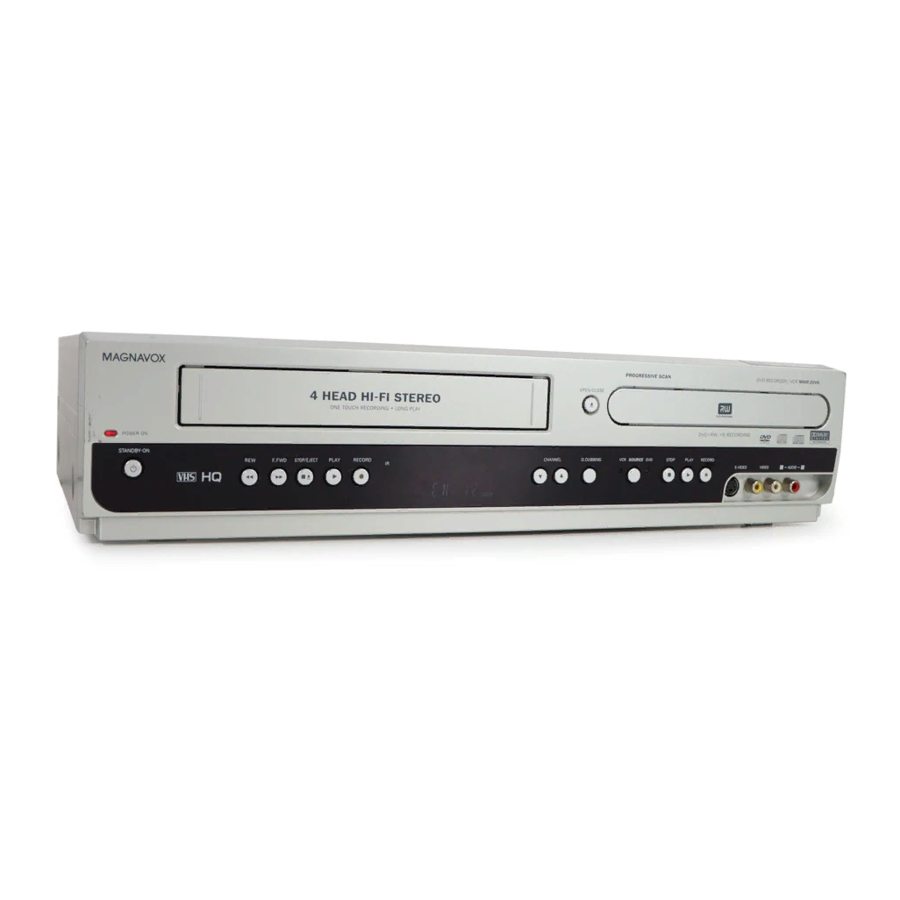
MWR20V6
When servicing the deck
mechanism, refer to MK14 Deck
Mechanism Section.
Deck Mechanism Part No.:
N2460FL
Advertisement
Table of Contents

Related Manuals for Magnavox MWR20V6


Summary of Contents for Magnavox MWR20V6
- Page 1 When servicing the deck I Specifications mechanism, refer to MK14 Deck I Preparation for Servicing Mechanism Section. I Adjustment Procedures I Schematic Diagrams Deck Mechanism Part No.: I CBA’s I Exploded Views N2460FL I Parts List DVD RECORDER & VIDEO CASSETTE RECORDER MWR20V6...
- Page 2 IMPORTANT SAFETY NOTICE Proper service and repair is important to the safe, reliable operation of all Funai Equipment. The service procedures recommended by Funai and described in this service manual are effective methods of performing service operations. Some of these service special tools should be used when and as recommended.
-
Page 3: Table Of Contents
MAIN SECTION DVD RECORDER & VIDEO CASSETTE RECORDER MWR20V6 Main Section I Specifications I Preparation for Servicing I Adjustment Procedures I Schematic Diagrams I CBA’s I Exploded Views I Parts List TABLE OF CONTENTS Specifications ................1-1-1 Laser Beam Safety Precautions . -
Page 4: Specifications
SPECIFICATIONS < VCR Section > Description Unit Minimum Nominal Maximum Remark 1. Video 1-1. Video Output (PB) Vp-p SP Mode 1-2. Video Output (R/P) Vp-p SP Mode, 1-3. Video S/N Y (R/P) W/O Burst 1-4. Video Color S/N AM (R/P) SP Mode 1-5. - Page 5 < DVD Section > ITEM CONDITIONS UNIT NOMINAL LIMIT 1. VIDEO 1-1. Video Output 75 ohm load Vp-p 1-2. S-Video Output Y (Luminance) 75 ohm load Vp-p C (Chrominance) 75 ohm load Vp-p 0.286 1-3. Component Output Y (Luminance) 75 ohm load Vp-p Cb (Chrominance) 75 ohm load...
-
Page 6: Laser Beam Safety Precautions
LASER BEAM SAFETY PRECAUTIONS This DVD player uses a pickup that emits a laser beam. Do not look directly at the laser beam coming from the pickup or allow it to strike against your skin. The laser beam is emitted from the location shown in the figure. When checking the laser diode, be sure to keep your eyes at least 30 cm away from the pickup lens when the diode is turned on. -
Page 7: Important Safety Precautions
IMPORTANT SAFETY PRECAUTIONS Product Safety Notice Also check areas surrounding repaired locations. J. Be careful that foreign objects (screws, solder Some electrical and mechanical parts have special droplets, etc.) do not remain inside the set. safety-related characteristics which are often not K. - Page 8 Safety Check after Servicing Examine the area surrounding the repaired location for damage or deterioration. Observe that screws, parts, and wires have been returned to their original positions. Afterwards, do the following tests and confirm the specified values to verify compliance with safety standards. 1.
-
Page 9: Standard Notes For Servicing
STANDARD NOTES FOR SERVICING Circuit Board Indications Pb (Lead) Free Solder 1. The output pin of the 3 pin Regulator ICs is When soldering, be sure to use the Pb free solder. indicated as shown. How to Remove / Install Flat Pack-IC Top View Bottom View 1. - Page 10 3. The flat pack-IC on the CBA is affixed with glue, so With Soldering Iron: be careful not to break or damage the foil of each 1. Using desoldering braid, remove the solder from pin or the solder lands under the IC when all pins of the flat pack-IC.
- Page 11 2. Installation With Iron Wire: 1. Using desoldering braid, remove the solder from 1. Using desoldering braid, remove the solder from all pins of the flat pack-IC. When you use solder the foil of each pin of the flat pack-IC on the CBA flux which is applied to all pins of the flat pack-IC, so you can install a replacement flat pack-IC more you can remove it easily.
- Page 12 Instructions for Handling Semi- conductors Electrostatic breakdown of the semi-conductors may occur due to a potential difference caused by electrostatic charge during unpacking or repair work. 1. Ground for Human Body Be sure to wear a grounding band (1 MΩ) that is properly grounded to remove any static electricity that may be charged on the body.
-
Page 13: Preparation For Servicing
PREPARATION FOR SERVICING How to Enter the Service Mode About Optical Sensors Caution: An optical sensor system is used for the Tape Start and End Sensors on this equipment. Carefully read and follow the instructions below. Otherwise the unit may operate erratically. What to do for preparation Insert a tape into the Deck Mechanism Assembly and press the PLAY button. -
Page 14: Cabinet Disassembly Instructions
CABINET DISASSEMBLY INSTRUCTIONS 1. Disassembly Flowchart REMOVAL This flowchart indicates the disassembly steps to gain REMOVE/*UNHOOK/ LOC. PART Fig. access to item(s) to be serviced. When reassembling, UNLOCK/RELEASE/ Note follow the steps in reverse order. Bend, route, and UNPLUG/DESOLDER dress the cables as they were originally. Rear Panel 6(S-6), 3(S-7), (S-8), Unit... - Page 15 Reference Notes CAUTION 1: Locking Tabs (L-1) and (L-2) are fragile. [5] Jack Bracket Be careful not to break them. (S-4) 1-1. Release five Locking Tabs (L-1). 1-2. Release three Locking Tabs (L-2) 1-3. Disconnect Connector (CN1609), and remove the Front Assembly. 2.
- Page 16 (S-7) (S-14) (S-13) (S-14) (S-8) (S-13) (S-6) (S-13) (S-14) (S-15) [8] Rear (S-7) (S-14) Panel Unit (S-14) (S-14) (S-16) (S-7) (S-12) [14] VCR Chassis Unit CN102 CN101 [13] Bracket R Fig. D5 Fig. D7 [12] Rear Panel (S-11) (S-10) (S-11) [10] DC Fan Motor AC Cord Hook...
- Page 17 Cylinder Assembly FE Head ACE Head Assembly SW512 LD-SW [15] Deck Assembly [16] Power SW CBA [17] Function [18] Main CBA [15] Deck Assembly (S-17) Cam Gear [18] Main Hole Lead Shaft with (S-18) blue Desolder stripe Hole LD-SW [18] Main CBA Desolder Lead with blue stripe...
- Page 18 (S-19) (S-19) [19] Deck Pedestal [20] Front Bracket R (S-20) Fig. D9 3. How to Eject Manually Note: When rotating the gear, be careful not to damage the gear. 1. Remove the Top Cover. 2. Rotate the gear in the direction of the arrow manually as shown below until the tray descends. 3.
-
Page 19: Electrical Adjustment Instructions
ELECTRICAL ADJUSTMENT INSTRUCTIONS General Note: “CBA” is abbreviation for Head Switching Position “Circuit Board Assembly.” Adjustment NOTE: Purpose: To determine the Head Switching position 1. Electrical adjustments are required after replacing during playback. circuit components and certain mechanical parts. Symptom of Misadjustment: May cause Head It is important to do these adjustments only after Switching noise or vertical jitter in the picture. -
Page 20: How To Initialize The Dvd Recorder & Vcr
HOW TO INITIALIZE THE DVD RECORDER & VCR To put the program back at the factory-default, initialize the DVD recorder & VCR as the following procedure. < DVD Section > 1. Turn the DVD recorder on. 2. Confirm that no disc is loaded or that the disc tray is open. -
Page 21: Firmware Renewal Mode
FIRMWARE RENEWAL MODE 1. Turn the power on and remove the disc on the tray. 4. Select the firmware version pressing arrow buttons, then press [OK]. 2. To put the DVD recorder into version up mode, Fig. d appears on the screen and Fig. e appears press [DVD], [CM SKIP], [6], [5], and [4] buttons on on the VFD. -
Page 22: Function Indicator Symbols
FUNCTION INDICATOR SYMBOLS < VCR Section > Note: If a mechanical malfunction occurs, the power is turned off. When the power comes on again after that by pressing [STANDBY-ON] button, an error message is displayed on the TV screen for 5 seconds. Led Mode Indicator Active When reel or capstan mechanism is not... - Page 23 < DVD Section > Note: If an error occurs, a message with the error number appears on the screen. Recording Error Error message You cannot record on this disc as Power Calibration Area is full. Error No. Error Message Solution Error Description Priority An error occurs during data reading.
- Page 24 Error Message Solution Error Description Priority During the CGMS picture (possible to This program is not allowed to Insert a ver.1.1 CPRM record once) input. (Disc which is not for be recorded on this disc. compatible DVD-RW disc. the correspondence to VR Format CPRM) Release the disc protect This disc is protected and not...
-
Page 25: Block Diagrams
BLOCK DIAGRAMS System Control Block Diagram 1-11-1 E9A80BLS... - Page 26 Servo Block Diagram 1-11-2 E9A80BLSV...
- Page 27 Digital Signal Process Block Diagram 1-11-3 E9A80BLD...
- Page 28 Video Block Diagram 1-11-4 E9A80BLV...
- Page 29 Video Input Select Block Diagram 1-11-5 E9A80BLVIS...
- Page 30 Video Output Select Block Diagram 1-11-6 E9A80BLVOS...
- Page 31 Audio Block Diagram E9A80BLA 1-11-7...
- Page 32 Audio Input/Output Select Block Diagram 1-11-8 E9A80BLAS...
- Page 33 Hi-Fi Audio Block Diagram E9A80BLH 1-11-9...
- Page 34 Power Supply Block Diagram 1-11-10 E9A80BLP...
-
Page 35: Schematic Diagrams / Cba's And Test Points
SCHEMATIC DIAGRAMS / CBA’S AND TEST POINTS Standard Notes WARNING Many electrical and mechanical parts in this chassis have special characteristics. These characteristics often pass unnoticed and the protection afforded by them cannot necessarily be obtained by using replacement components rated for higher voltage, wattage, etc. - Page 36 LIST OF CAUTION, NOTES, AND SYMBOLS USED IN THE SCHEMATIC DIAGRAMS ON THE FOLLOWING PAGES: 1. CAUTION: FOR CONTINUED PROTECTION AGAINST FIRE HAZARD, REPLACE ONLY WITH THE SAME TYPE FUSE. ATTENTION: POUR UNE PROTECTION CONTINUE LES RISQES D'INCELE N'UTILISER QUE DES FUSIBLE DE MÊME TYPE. RISK OF FIRE-REPLACE FUSE AS MARKED.
- Page 37 Main 1/7 Schematic Diagram < VCR Section > 1-12-3 E9A80SCM1...
- Page 38 Main 2/7, Power SW, DVD Open/Close SW & Sensor Schematic Diagram < VCR Section > FIP501 MATRIX CHART P.SCAN VCD VCR REPEAT VCD VCR XP SP LP EP REPEAT P.SCAN 1-12-4 E9A80SCM2...
- Page 39 Main 3/7 Schematic Diagram < VCR Section > 1-12-5 E9A80SCM3...
- Page 40 Main 4/7 Schematic Diagram < VCR Section > 1-12-6 E9A80SCM4...
- Page 41 Main 5/7 Schematic Diagram < VCR Section > 1-12-7 E9A80SCM5...
- Page 42 Main 6/7 Schematic Diagram < VCR Section > 1-12-8 E9A80SCM6...
- Page 43 Main 7/7 Schematic Diagram < VCR Section > 1-12-9 E9A80SCM7...
- Page 44 Power Supply & Junction Schematic Diagram < VCR Section > CAUTION ! CAUTION ! NOTE: For continued protection against fire hazard, Fixed voltage (or Auto voltage selectable) power supply circuit is used in this unit. The voltage for parts in hot circuit is measured using replace only with the same type fuse.
- Page 45 Front Jack Schematic Diagram < VCR Section > 1-12-11 E9A80SCJK...
- Page 46 DVD Main 1/5 Schematic Diagram < DVD Section > NOTE: 1. The order of pins shown in this diagram is different from that of actual IC101. 2. IC101 is divided into five and shown as IC101 (1/5) ~ IC101 (5/5) in this DVD Main Schematic Diagram Section. 1-12-12 E9A80SCD1...
- Page 47 DVD Main 2/5 Schematic Diagram < DVD Section > NOTE: 1. The order of pins shown in this diagram is different from that of actual IC101. 2. IC101 is divided into five and shown as IC101 (1/5) ~ IC101 (5/5) in this DVD Main Schematic Diagram Section. 1-12-13 E9A80SCD2...
- Page 48 DVD Main 3/5 Schematic Diagram < DVD Section > NOTE: 1. The order of pins shown in this diagram is different from that of actual IC101. 2. IC101 is divided into five and shown as IC101 (1/5) ~ IC101 (5/5) in this DVD Main Schematic Diagram Section. 1-12-14 E9A80SCD3...
- Page 49 DVD Main 4/5 Schematic Diagram < DVD Section > NOTE: 1. The order of pins shown in this diagram is different from that of actual IC101. 2. IC101 is divided into five and shown as IC101 (1/5) ~ IC101 (5/5) in this DVD Main Schematic Diagram Section. 1-12-15 E9A80SCD4...
- Page 50 DVD Main 5/5 Schematic Diagram < DVD Section > NOTE: 1. The order of pins shown in this diagram is different from that of actual IC101. 2. IC101 is divided into five and shown as IC101 (1/5) ~ IC101 (5/5) in this DVD Main Schematic Diagram Section. 1-12-16 E9A80SCD5...
- Page 51 Main CBA Top View Sensor CBA Top View TO SENSOR CBA (END-SENSOR) TP751 BHF300F01012A TO SENSOR CBA V-OUT (START-SENSOR) BHF300F01012B TP301 C-PB VR501 SW-P TP513 TP302 RF-SW TP502 S-INH 1-12-17 BE9A00F01011A...
- Page 52 Main CBA Bottom View PIN 2 OF IC1406 WF11 PIN 1 OF TU900 WF12 PIN 5 OF TU900 WF13 PIN 10OF TU900 WF14 PIN 11 OF TU900 WF15 PIN 17 OF TU900 WF10 PIN 28 OF CN2204 PIN 14 OF CN201 PIN 22 OF CN201...
- Page 53 Power Supply CBA Top View CAUTION ! CAUTION ! For continued protection against fire hazard, Fixed voltage (or Auto voltage selectable) power supply circuit is used in this unit. replace only with the same type fuse. If Main Fuse (F1001) is blown , check to see that all components in the power supply ATTENTION : Pour une protection continue les risqes circuit are not defective before you connect the AC plug to the AC power supply.
- Page 54 Power Supply CBA Bottom View CAUTION ! CAUTION ! For continued protection against fire hazard, Fixed voltage (or Auto voltage selectable) power supply circuit is used in this unit. replace only with the same type fuse. If Main Fuse (F1001) is blown , check to see that all components in the power supply ATTENTION : Pour une protection continue les risqes circuit are not defective before you connect the AC plug to the AC power supply.
- Page 55 Power SW CBA Top View Power SW CBA Bottom View DVD Open/Close SW CBA Top View DVD Open/Close SW CBA Bottom View BE9A00F01011B BE9A00F01011C Front Jack CBA Top View Front Jack CBA Bottom View Junction CBA Top View Junction CBA Bottom View BE9A00F01011D BE9A00F01021B 1-12-21...
-
Page 56: Waveforms
WAVEFORMS NOTE: Input: COLOR BAR SIGNAL (WITH 1KHz AUDIO SIGNAL) TP751 WF11 Pin 1 of TU900 Pin 2 of IC1406 MOD-A 0.5V 0.2ms V-OUT E-E 0.2V 20µs VIDEO-CVBS 0.5V 20µs TP751 UPPER WF12 Pin 28 of CN201 Pin 5 of TU900 TP302 LOWER V-OUT... -
Page 57: Wiring Diagram < Vcr Section
WIRING DIAGRAM < VCR SECTION > 1-14-1 E9A80WI... -
Page 58: Wiring Diagram < Dvd Section
WIRING DIAGRAM < DVD SECTION > 1-14-2 E9A80WID... -
Page 59: System Control Timing Charts
SYSTEM CONTROL TIMING CHARTS < VCR Section > Mode SW: LD-SW LD-SW Position detection A/D Input voltage Limit Symbol (Calculated voltage) 3.76 V ~ 4.50 V (4.12 V) 4.51 V ~ 5.00 V (5.00 V) 0.00 V ~ 0.25 V (0.00 V) 1.06 V ~ 1.50 V (1.21 V) 0.66 V ~ 1.05 V (0.91 V) 1.99 V ~ 2.60 V (2.17 V) - Page 60 Still/Slow Control Frame Advance Timing Chart 1) SP Mode 23 RF-SW The first rise of RF-SW after a rise in F-AD signal F-AD (Internal Signal) "H" "H" "Z" C-DRIVE "L" "L" Stop detection (T2) Acceleration Detection (T1) Slow Tracking Value PB CTL Reversal Limit Value 20ms...
- Page 61 2) LP/SLP Mode 23 RF-SW The first rise of RF-SW after a rise in F-AD signal F-AD (Internal Signal) "H" "H" "Z" C-DRIVE "L" "L" Stop detection (T2) Acceleration Detection (T1) Slow Tracking Value PB CTL Reversal Limit Value 20ms 32 C-F/R 99 H-A-SW 98 C-ROTA...
- Page 62 EJECT ST-S/ END-S "OFF" CASS.LOAD LD-FWD 0.2S LD-REV 0.7S LD-FWD 0.4S LD-FWD 0.2S LD-REV 0.2S LD-FWD 0.5S LD-REV STOP(A) PLAY LD-FWD PLAY LD-FWD LD-REV 0.2S LD-FWD PLAY PLAY PAUSE (SLOW) LD-FWD STILL(SLOW) PLAY LD-REV 0.2S LD-FWD PLAY STOP /EJECT LD-REV STOP(A) Fig.
- Page 63 STOP(A) STOP LD-REV 0.2S LD-FWD STOP /EJECT 1.0S LD-FWD 0.5S LD-REV STOP(A) LD-REV 0.2S LD-FWD STOP /EJECT LD-REV 1.0S LD-FWD 0.5S LD-REV STOP(A) LD-FWD PAUSE LD-FWD 2.5S Short REV LD-REV 0.2S LD-FWD REC PAUSE REC or PAUSE STOP /EJECT LD-FWD 1.5S LD-REV 0.2S...
- Page 64 < DVD Section > [ Tray Open ] Power on Push Close button is pressed. Tray insertion INNER-SW Case 3 open? [ open ] button is pressed. Is Timer Case 1 Is slit S5 ET3 passed? passed? Rezero 1 Rezero 2 Case 4 Is Timer [ open ] button is pressed.
- Page 65 Parameter S*: Encoder pulse ET*: Error V*: Voltage (HEX) T*: Event timer (HEX) detection timer V0: 2.0 V (00d) S1: 300 (12c) T1: 0.1 s ET1: 5.0 s V1: 4.5 V (022) S2: 3300 (ce4) T2: 3.0 s ET2: 5.0 s V2: 2.2 V (010) S3: 3935 (f5f) T3: 3.0 s...
- Page 66 Tray close Tray ejection direction SLED Tray insersion direction open INNER-SW close Timer Push close Push Close Encoder pulse SLED Tray insersion direction open INNER-SW close Timer 1-15-8 W3N4HTI...
- Page 67 Case 1 SLED Tray insersion direction open INNER-SW close Timer Rezero 1 Case 2 Tray ejection direction SLED Tray insersion direction open INNER-SW close Rezero 2 Case 3 (When [OPEN] button is pressed before the S5 passage.) Encoder pulse Tray ejection direction SLED Timer Case 4 (When [OPEN] button is pressed after the S5 passage.)
- Page 68 Case 5 (Retry.) Tray ejection direction SLED Tray insersion direction open INNER-SW close Start retry. Retry frequency 1st time retry 2nd time retry 3rd time retry 4th time retry 5th time retry 6th time retry 1-15-10 W3N4HTI...
-
Page 69: Ic Pin Function Descriptions
IC PIN FUNCTION DESCRIPTIONS < VCR Section > Signal Function Name IC501 (SERVO/SYSTEM CONTROL/OSD) System Reset Signal IN RESET (Reset=”L”) “H” ≥ 4.5 V, “L” ≤ 1.0 V LM-FWD/ Loading Motor FWD/ REV 26 OUT Signal Output Function Name 27 OUT P-ON-L Power On Signal to Low P-DOWN Power Voltage Down Detector... - Page 70 Signal Signal Function Function Name Name Low Path Filter Input Signal IN AFCC VCR Power Supply Safety For AFC POWER- Signal SAFETY Low Path Filter Output Signal 53 OUT AFCLPF For AFC Tape End Position Detect IN END-S Signal VIDEO- 54 OUT Video Mute Control Signal MUTE...
- Page 71 < DVD Section > IC571 (FIP DRIVER IC) Signal Function Name IN CLK Clock Input IN STB Serial Interface Strobe Not Used Not Used Power Supply Segment Output Pull Down Level 16 OUT i Segment Output Grid Output Power Supply IN OSC Oscillator Input Not Used...
-
Page 72: Lead Identifications
LEAD IDENTIFICATIONS KRA103M-AT/P KTC3198-Y-AT/P PQ070XF01SZH 2SK3563 KRC103M-AT/P KTC3203-Y-AT/P KTA1267Y-AT/P 2SC3266-GR(TPE2 F) KTC3193-Y-AT/P KTC3199-(BL,Y)-AT/P KTA1266-Y-AT/P PS2561A-1(W) 1: Anode 1 2 3 4 2: Cathode G D S 3: Emitter E C B E C B 4: Collector CD4052BNSR MM1636XWRE PT6313-S-TP(L) MM1697AJBE KIA4558P/P CD4053BNSR RC4580IP... -
Page 73: Exploded Views
EXPLODED VIEWS Cabinet 2L011 2L011 2L071 See Electrical Parts List 2L071 2L071 for parts with this mark. 2L071 2L081 2B35 2L011 AC1001 2L082 2L062 2L044 2L100 FM1001 2L081 2L044 2L044 2L033 Sensor CBA 2L011 2L045 2L033 2B14 2L033 Power Supply CBA Sensor CBA Power SW CBA 2L045... - Page 74 Packing Unit Some Ref. Numbers are not in sequence. 2B64 1-18-2 E9A80PEX...
-
Page 75: Mechanical Parts List
MECHANICAL PARTS LIST PRODUCT SAFETY NOTE: Products marked with a Ref. No. Description Part No. # have special characteristics important to safety. FM1001 DC FAN MOTOR D06K-12TS7 01(AX) MMEZR12NH003 Before replacing any of these components, read PACKING carefully the product safety notice in this service GIFT BOX CARTON E9A80UD 1VM322230 manual. -
Page 76: Electrical Parts List
ELECTRICAL PARTS LIST PRODUCT SAFETY NOTE: Products marked with a Ref. No. Description Part No. # have special characteristics important to safety. C308 ELECTROLYTIC CAP . 47µF/6.3V M H7 CE0KMAVSL470 Before replacing any of these components, read C309 CHIP CERAMIC CAP .(1608) F Z 0.1µF/50V CHD1JZ30F104 carefully the product safety notice in this service C310... - Page 77 Ref. No. Description Part No. Ref. No. Description Part No. C461 CHIP CERAMIC CAP .(1608) B K 0.01µF/50V CHD1JK30B103 C839 ELECTROLYTIC CAP . 1µF/50V M CE1JMASDL1R0 C462 CHIP CERAMIC CAP .(1608) B K 0.01µF/50V CHD1JK30B103 C840 CHIP CERAMIC CAP .(1608) B K 0.1µF/50V CHD1JK30B104 C465 ELECTROLYTIC CAP .
- Page 78 Ref. No. Description Part No. Ref. No. Description Part No. C1536 ELECTROLYTIC CAP . 22µF/6.3V M H7 CE0KMASSL220 L771 PCB JUMPER D0.6-P5.0 JW5.0T C1537 CHIP CERAMIC CAP .(1608) F Z 0.1µF/50V CHD1JZ30F104 L800 PCB JUMPER D0.6-P5.0 JW5.0T CONNECTORS L801 PCB JUMPER D0.6-P5.0 JW5.0T L900 PCB JUMPER D0.6-P5.0...
- Page 79 Ref. No. Description Part No. Ref. No. Description Part No. CHIP RES. 1/10W J 4.7k Ω CHIP RES. 1/10W J 3.3k Ω R117 RRXAJR5Z0472 R458 RRXAJR5Z0332 CHIP RES. 1/10W J 47k Ω CHIP RES. 1/10W J 39k Ω R118 RRXAJR5Z0473 R459 RRXAJR5Z0393 CARBON RES.
- Page 80 Ref. No. Description Part No. Ref. No. Description Part No. CHIP RES. 1/10W J 3.9k Ω CHIP RES. 1/10W J 4.7k Ω R606 RRXAJR5Z0392 R875 RRXAJR5Z0472 CHIP RES. 1/10W J 8.2k Ω CHIP RES. 1/10W J 4.7k Ω R607 RRXAJR5Z0822 R876 RRXAJR5Z0472 CHIP RES.
- Page 81 Ref. No. Description Part No. Ref. No. Description Part No. CHIP RES.(1608) 1/10W 0 Ω CHIP RES. 1/10W J 75 Ω JC31 RRXAJR5Z0000 R815 RRXAJR5Z0750 CHIP RES.(1608) 1/10W 0 Ω JC38 RRXAJR5Z0000 MISCELLANEOUS JK751 RCA JACK MSP-213V1-324-B NI L JXRL030LY104 JK800 RCA JACK(RED) MTJ-032-11A-31 FE01 JYRL010LY024...
- Page 82 Ref. No. Description Part No. Ref. No. Description Part No. D021 SCHOTTKY BARRIER DIODE SB340 NDQZ000SB340 FH1001 FUSE HOLDER MSF-015 LF (B110) XH01Z00LY002 D022 SCHOTTKY BARRIER DIODE SB140 NDQZ000SB140 FH1002 FUSE HOLDER MSF-015 LF (B110) XH01Z00LY002 D023 RECTIFIER DIODE FR101 NDWZ000FR101 T001# TRANS POWER BCK-28-0663...
- Page 83 MWR20V6 E9A80UD 2006-03-24...