Table of Contents
Advertisement
SERVICE MANUAL
Ver. 1.0 2017.03
Note:
Be sure to keep your PC used for service and
checking of this unit always updated with the
latest version of your anti-virus software.
In case a virus affected unit was found during
service, contact your Service Headquarters.
AUDIO POWER SPECIFICATIONS
POWER OUTPUT AND TOTAL
HARMONIC DISTORTION:
(US models only)
With 5 ohm loads, both channels driven,
from 280 Hz – 20,000 Hz; rated 70 watts per
channel minimum RMS power, with no more
than 0.7% total harmonic distortion from 250
milliwatts to rated output.
Speaker section
Speaker system:
3-way, Sound Pressure Horn
Speaker unit:
Tweeter L/R: 40 mm (1
5
/
in), cone type
8
Midrange L/R: 80 mm (3
/
in), cone type
1
4
Woofer: 200 mm (7
7
/
in), cone type
8
Rated impedance:
Tweeter L/R: 5 ohms
Midrange L/R: 5 ohms
Woofer: 2 ohms
Inputs
AUDIO/PARTY CHAIN IN L/R (V50):
Voltage 2 V, impedance
47 kilohms
AUDIO/PARTY CHAIN IN (TV) L/R (V50D):
Voltage 2 V, impedance
47 kilohms
TV (ARC) (V50D):
Supported audio signal:
2-channel Linear PCM
MIC1:
Sensitivity 1 mV, impedance
10 kilohms
MIC2/GUITAR:
Sensitivity 1 mV, impedance
10 kilohms (When guitar mode is
turned off.)
Sensitivity 200 mV, impedance
1 Megaohm (When guitar mode is
turned on.)
Outputs
AUDIO/PARTY CHAIN OUT L/R:
Voltage 2 V, impedance 1 kilohm
VIDEO OUT (V50D):
Max. output level 1 Vp-p,
unbalanced, Sync. negative load
impedance 75 ohms
HDMI OUT (TV) (V50D):
Supported audio signal:
2-channel Linear PCM (up to 48 kHz),
Dolby Digital
9-890-684-01
Sony Corporation
2017C81-1
©
2017.03
Published by Sony EMCS (Malaysia) PG Tec
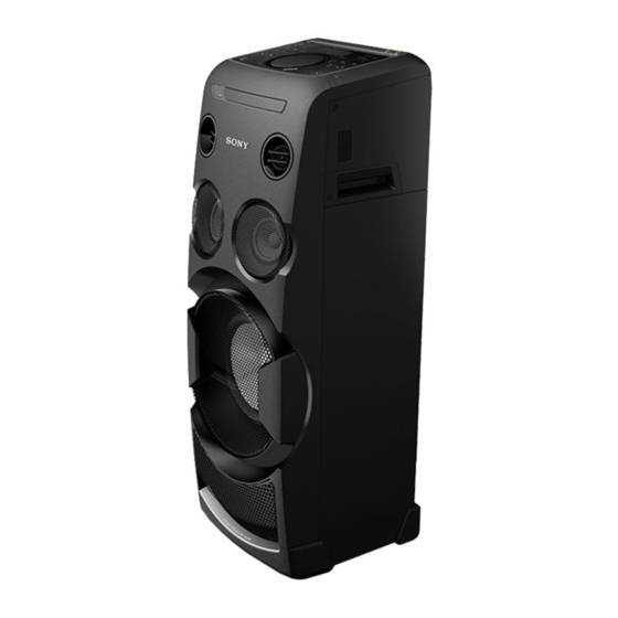
MHC-V50/V50D
Photo: MHC-V50D
Model Name Using Similar Mechanism
CD/DVD Section
CD Mechanism Type
Optical Pick-up Name
SPECIFICATIONS
HDMI section (V50D)
Connector:
Type A (19 pin)
Disc player section
System:
Compact disc and digital audio
system (V50)
Compact disc and digital audio and
video system (V50D)
Laser Diode Properties
Emission Duration: Continuous
Laser Output*: Less than 44.6 μW
* This output is the value measure-
ment at a distance of 200 mm
from the objective lens surface on
the Optical Pick-up Block with
7 mm aperture.
Frequency response:
20 Hz – 20 kHz
Video color system format
Latin American model:
NTSC
Other models:
NTSC and PAL
USB section
Supported USB device:
Mass Storage Class
Maximum current:
1 A
(USB) port:
Type A
FM Tuner section
FM stereo, FM superheterodyne tuner
Antenna:
FM lead antenna
Tuning range:
87.5 MHz – 108.0 MHz (50 kHz step)
BLUETOOTH section
Communication system:
BLUETOOTH Standard version 3.0
Output:
BLUETOOTH Standard Power
Class 2
Maximum communication range:
Line of sight approx. 10 m (33 ft)*
1
Frequency band:
2.4 GHz band (2.4000 GHz –
2.4835 GHz)
Modulation method:
FHSS (Freq Hopping Spread
Spectrum)
MHC-V44D
CDM90-DVBU204//C
CMS-S76RFS7G1 or CMS-S76RFS7GP
Compatible BLUETOOTH profiles*
2
:
A2DP (Advanced Audio Distribu-
tion Profile)
AVRCP (Audio Video Remote
Control Profile)
SPP (Serial Port Profile)
Supported codecs:
SBC (Subband Codec)
AAC (Advanced Audio Coding)
LDAC
*
1
The actual range will vary depending on
factors such as obstacles between devices,
magnetic fields around a microwave oven,
static electricity, reception sensitivity,
antenna's performance, operating system,
software application, etc.
*
BLUETOOTH standard profiles indicate
2
the purpose of BLUETOOTH communica-
tion between devices.
Supported audio formats
Supported bit rate and sampling frequencies:
MP3:
32/44.1/48 kHz, 32 kbps –
320 kbps (VBR)
AAC:
44.1 kHz, 48 kbps – 320 kbps
(CBR/VBR)
WMA:
44.1 kHz, 48 kbps – 192 kbps
(CBR/VBR)
WAV:
44.1/48 kHz (16 bit)
Supported video formats (V50D)
Xvid:
Video codec: Xvid video
Bit rate: 4.854 Mbps (MAX)
Resolution/Frame rate:
720 × 480, 30 fps
720 × 576, 25 fps (except for Latin
American model)
Audio codec: MP3
MPEG4
File format: MP4 File Format
Video codec: MPEG4 Simple Profi le
(AVC is not compatible.)
Bit rate: 4 Mbps
Resolution/Frame rate:
HOME AUDIO SYSTEM
720 × 480, 30 fps
US Model
Canadian Model
MHC-V50
AEP Model
UK Model
E Model
Australian Model
MHC-V50D
720 × 576, 25 fps (except for Latin
American model)
Audio codec: AAC-LC (HE-AAC is
not compatible.)
DRM: Not compatible
General
Power requirements:
US, CND models:
AC 120 V, 60 Hz
Except US, CND models:
AC 120 V – 240 V, 50/60 Hz
Power consumption:
120 W
Power consumption (at the Power Saving
mode) (V50D):
0.5 W (When "BT STBY" is set to
"OFF" and [CONTROL FOR HDMI]
is set to [OFF].)
3 W* (When "BT STBY" is set to
"ON" and [CONTROL FOR HDMI]
is set to [ON].)
Dimensions (W/H/D) (Approx.):
293 mm × 798 mm × 300 mm
(11
5
/
in x 31
1
/
in x 11
7
/
in)
8
2
8
Mass (Approx.):
14 kg (30 lb 14 oz)
* The power consumption of the system will
be less than 0.5 W when there is no HDMI
connection and "BT STBY" is set to "OFF".
Unpacking
• This unit (MHC-V50/V50D) (1)
• Remote control (1)
• R03 (size AAA) batteries (2)
• FM lead antenna (1)
• AC power cord (mains lead) (1)
• AC plug adaptor* (1) (supplied only for
certain areas) (V50D)
* This plug adaptor is not for the use
in Chile, Paraguay and Uruguay. Use
this plug adaptor in the countries
where it is necessary.
Design and specifications are subject to
change without notice.
– Continued on next page –
Advertisement
Table of Contents

Related Manuals for Sony MHC-V50


Summary of Contents for Sony MHC-V50
- Page 1 720 × 480, 30 fps HDMI OUT (TV) (V50D): 2.4835 GHz) Supported audio signal: Modulation method: 2-channel Linear PCM (up to 48 kHz), FHSS (Freq Hopping Spread Spectrum) Dolby Digital 9-890-684-01 Sony Corporation 2017C81-1 © 2017.03 Published by Sony EMCS (Malaysia) PG Tec...
- Page 2 3. Measuring the voltage drop across a resistor by means of a • “BRAVIA” is a trademark of Sony Corporation. VOM or battery-operated AC voltmeter. The “limit” indication • LDAC™ and LDAC logo are trademarks of Sony Corporation. is 0.75 V, so analog meters must have an accurate low-voltage ®...
-
Page 3: Table Of Contents
MHC-V50/V50D TABLE OF CONTENTS ..........6-17. Printed Wiring Board - IR Board - ........49 SERVICING NOTES 6-18. Schematic Diagram - IR Board - ........49 6-19. Printed Wiring Board DISASSEMBLY 2-1. Disassembly Flow ............10 - TOP PARTY LIGHT Board - ........49 2-2. -
Page 4: Servicing Notes
MHC-V50/V50D SECTION 1 SERVICING NOTES UNLEADED SOLDER MODEL IDENTIFICATION Boards requiring use of unleaded solder are printed with the – Rear View – leadfree mark (LF) indicating the solder contains no lead. (Caution: Some printed circuit boards may not come printed with... - Page 5 (TIG2000) After you have checked and found no problems, reconnect the AC power cord (mains lead), and turn on the system. If the issue persists, contact your IC2003 nearest Sony dealer. thermal compound (TIG2000) IC2002...
- Page 6 6. Select model’s name on the display of the Bluetooth device. Start playback of an audio source on the smartphone. For For example, select “MHC-V50 or MHC-V50D”. If passkey details on playback, refer to the operating instructions of your is required on the Bluetooth device, enter “0000”.
- Page 7 MHC-V50/V50D HOW TO OPEN THE TRAY WHEN POWER SWITCH TURN OFF Note 1: After the side panel and top panel are removed, this work is done. Note 2: Please prepare the thin wire (clip etc. processed to the length of 8 cm or more).
- Page 8 MHC-V50/V50D CAPACITOR DISCHARGE FOR ELECTRIC SHOCK PREVENTION SMPS Board (Conductor side view) In checking the SMPS board, make 3 capacitors discharge of C914, C1003 and C1006 for eletrical shock prevention. C1003 800 /5 W C914 C1006 800 /5 W 800 /5 W DAMP Board (Conductor side view) In checking the DAMP board, make 1 capacitor discharge of C2076 for electrical shock prevention.
- Page 9 MHC-V50/V50D SERVICE POSITION top panel section VOLUME board CDM section IR board MIC board stand LCD board USB board stand SMPS board DAMP board insulating sheet MOTHERBOARD board...
-
Page 10: Disassembly
MHC-V50/V50D SECTION 2 DISASSEMBLY Note: Disassemble the unit in the order as shown below. 2-1. DISASSEMBLY FLOW 2-2. SIDE (L) PANEL, SIDE (R) PANEL (Page 11) 2-3. TOP PANEL SECTION (Page 12) 2-4. LOADING PANEL ASSY (Page 13) 2-5. CDM SECTION (Page 14) 2-6. -
Page 11: Side (L) Panel, Side (R) Panel
MHC-V50/V50D Note: Follow the disassembly procedure in the numerical order given. 2-2. SIDE (L) PANEL, SIDE (R) PANEL 1 one screw (SCREW, TAPPING) 3 two screws (+BVTP 3 x 8) 4 three claws 6 panel, side (R) 3 two screws... -
Page 12: Top Panel Section
MHC-V50/V50D 2-3. TOP PANEL SECTION ire ettin rear side MIC board TOP PARTY 1 one screw (+BVTP 3 x 8) LED board 1 one screw (+BVTP 3 x 8) q; flexible flat cable (6 core) (CN105) qg panel, top section... -
Page 13: Loading Panel Assy
MHC-V50/V50D 2-4. LOADING PANEL ASSY 3 three claws 4 panel, loading assy hole – Left view – Insert the clip etc. processed to the length of 8 cm or more in the hole on the side of the CDM and push. -
Page 14: Cdm Section
MHC-V50/V50D 2-5. CDM SECTION q; four screws (+BVTP 3 x 8) Note 1: When installing the flexible flat cable, ensure that the colored line is not slanted after insertion. Insert is straight to the interior. flexible flat cable qs CDM90-DVBU204//C... -
Page 15: Back Panel Section, Module Cover
MHC-V50/V50D 2-6. BACK PANEL SECTION, MODULE COVER Note: When you install the connector, please install them correctly. There is a possibility that this machine damages when not correctly installing it. hemilon, 10XLX0.4 Insert is straight Insert is shallow Insert is incline to the interior. -
Page 16: Damp Board
MHC-V50/V50D 2-7. DAMP BOARD 6 four screws (+BVTP 3 x 8) qa heatsink (AMP) Note: When you install the heatsink (AMP), spread the compound referring to ire e i “NOTE OF REPLACING THE IC2002 front side AND IC2003 ON THE DAMP BOARD AND THE COMPLETE DAMP BOARD”... -
Page 17: Bracket Chassis
MHC-V50/V50D 2-8. BRACKET CHASSIS 1 hemilon, 10XLX0.4 5 five screws (+BV3 (3-CR)) front side 3 Remove the wires from 8 CN2002 (11P) clip, coating. 9 bracket, chassis MOTHERBOARD board clip, coating front side 6 Remove bracket, 7 Draw out the wire from chassis in the bracket, chassis. -
Page 18: Motherboard Board
MHC-V50/V50D 2-9. MOTHERBOARD BOARD Note: When the MOTHERBOARD BOARD is replaced, refer to “NOTE OF REPLACING MOTHERBOARD BOARD OR BLUE- TOOTH MODULE OR RC-S730 (WW) BOARD” on page 6. 1 five screws (+BVTP 3 x 8) 2 clip, coating 2 clip, coating... -
Page 19: Smps Board
MHC-V50/V50D 2-10. SMPS BOARD 2 three screws (+PWH 3 x 8 (SUMITITE)) 1 six screws (+PWH 3 x 8 (SUMITITE)) 3 SMPS board – Rear view – 2-11. CHASSIS 1 six screws (STEP SCREW M4) 2 one claw 2 one claw 3 chassis –... -
Page 20: Front Panel Section
MHC-V50/V50D 2-12. FRONT PANEL SECTION 1 one screw ((3.5 x 16), TAPPING) total sixteen bosses 3 Insert the jig into a space and slowly 3 Insert the jig into a space and slowly remove the front panel section. Note 1: When using a jig, please work remove the front panel section. -
Page 21: Loudspeaker (20Cm)
MHC-V50/V50D 2-13. LOUDSPEAKER (20CM) 3 Push the protrusion, and remove the terminal (wide side). top side protrusion 3 Push the protrusion, and remove loudspeaker the terminal (narrow side). (20CM) terminal (narrow side) terminal (wide side) loudspeaker (20CM) terminal position 2 Remove the loudspeaker (20CM) in the direction of the arrow. -
Page 22: Loudspeaker (8Cm)
MHC-V50/V50D 2-14. LOUDSPEAKER (8CM) 4 Push the protrusion, and remove the terminal (wide side). hook hook terminal (wide side) terminal (narrow side) 1 Remove the speaker cable. protrusion 4 Push the protrusion, and remove the terminal (narrow side). 3 Remove the loudspeaker... -
Page 23: Service Optical Device (7G), Flexible Flat Cable
MHC-V50/V50D 2-15. SERVICE OPTICAL DEVICE (7G), FLEXIBLE FLAT CABLE 2 chuck holder assy (MB) qf cushion (H) 1 three claws qj filament tape qg filament tape 1 three claws 7 four insulator screws qa insulator qk cushion (H) w; holder, flexible flat cable... -
Page 24: Test Mode
3. “COLD RST” appears on the screen display panel. After that, This is the display check mode. “SONY DEMO” appears on the screen display panel. The Touch [ENTER] touch key repeatedly to toggle different system automatically turn on and off once. Please be sure that display mode as below: the system stay at demo mode fi... -
Page 25: Electrical Check
MHC-V50/V50D SECTION 4 ELECTRICAL CHECK FOCUS BIAS CHECK TUNER SECTION 0 dB = 1 V oscilloscope FM AUTO STOP CHECK (DC range) signal MOTHERBOARD board generator CN302 pin 17 (RF) CN302 pin 1 (GND) – Procedure: 1. Connect the oscilloscope to CN302 pin 17 (RF) and CN302 pin 1 (GND) on the MOTHERBOARD board. -
Page 26: Troubleshooting
MHC-V50/V50D SECTION 5 TROUBLESHOOTING... - Page 27 MHC-V50/V50D...
- Page 28 MHC-V50/V50D...
- Page 29 MHC-V50/V50D...
- Page 30 MHC-V50/V50D...
- Page 31 MHC-V50/V50D...
-
Page 32: Diagrams
MHC-V50/V50D SECTION 6 DIAGRAMS • Circuit Boards Location TOP PARTY LIGHT board LCD board BACK PARTY LIGHT L board USB board PARTY LIGHT DRIVER board VOLUME board BACK PARTY LIGHT R board SENSOR board MIC board IR board MOTHERBOARD board... -
Page 33: Block Diagram - Cd/Usb/Hdmi Section
MHC-V50/V50D 6-1. BLOCK DIAGRAM - CD/USB/HDMI Section - >001B MAIN SECTION (Page 34) >002B MAIN SECTION (Page 34) V D D RF_D V50D F R D F _ D_ D F _ D_ F R DVD F _ D_DVD 50... -
Page 34: Block Diagram - Main Section
MHC-V50/V50D 6-2. BLOCK DIAGRAM - MAIN Section - STEREO A/D CONVERTER NFC MODULE (RC-S730 (WW)) IC904 >002B NFC-SCL RXIN0 CD/USB/HDMI SECTION MKT-BCK MKT-BCK NFC-SDA (Page 33) RXIN5/ABCK0I MKT-LRCK MKT-LRCK NFC-INT RXIN6/ALRCK0I ASDATA0 ASDATA0 NFC-RF-DET RXIN7/ADIN0 J602 MKT-MCK VINL VINR BUS BUFFER... -
Page 35: Block Diagram - Damp Section
MHC-V50/V50D 6-3. BLOCK DIAGRAM - DAMP Section - STREAM PROCESSOR POWER AMP IC2001 IC2002 >003B MAIN SECTION 11 MCLK PWM_P_4 5 INPUT_A OUT_D_27 (Page 34) LRCK TWEETER 22 LRCLK PWM_M_4 6 INPUT_B OUT_D_28 L-CH SCLK 23 SCLK PWM_P_3 14 INPUT_C... -
Page 36: Block Diagram - Touch/Led Driver Section
MHC-V50/V50D 6-4. BLOCK DIAGRAM - TOUCH/LED DRIVER Section - SYSTEM CONTROLLER LED DRIVER LED DRIVER IC109 (4/5) IC1000 IC1003 SIN_VOL D1211 - D1225 SOUT 22 VOL_WLED_8 D1002,D1004,D1005 M+5.2V OUT8 13 RGB1_RED VOL_WLED_4 OUT9 14 M+13V OUT9 14 TOUCH SENSOR CONTROLER... -
Page 37: Block Diagram - Panel/Power Supply Section
MHC-V50/V50D 6-5. BLOCK DIAGRAM - PANEL/POWER SUPPLY Section - SYSTEM CONTROLLER IC109 (5/5) REMOTE CONTROL RECEIVER IC2200 PROTECTION CONTROL PCONT-DAMP Q576 SIRCS PROTECTION CONTROL Q575 +5V/ +5.2V REG. IC001 S1252 PROTECTION CONTROL POWER-KEY SPM-C-MON Q574 USB +5V VIN1 PROTECTION CONTROL M +5.2V... - Page 38 MHC-V50/V50D • Note for Printed Wiring Boards and Schematic Diagrams Note on Printed Wiring Board: Note on Schematic Diagram: • X : parts extracted from the component side. • All capacitors are in μF unless otherwise noted. (p: pF) •...
-
Page 39: Printed Wiring Board - Motherboard Board
MHC-V50/V50D 6-6. PRINTED WIRING BOARD - MOTHERBOARD Board - • See page 32 for Circuit Boards Location. • : Uses unleaded solder. MOTHERBOARD BOARD AUDIO/ MOTHERBOARD BOARD ANTENNA PARTY CHAIN HDMI OUT VIDEO (TV) ARC SERVICE ONLY (COMPONENT SIDE) (CONDUCTOR SIDE) -
Page 40: Printed Wiring Board - Damp Board
MHC-V50/V50D 6-7. PRINTED WIRING BOARD - DAMP Board - • See page 32 for Circuit Boards Location. • : Uses unleaded solder. DAMP BOARD DAMP BOARD (COMPONENT SIDE) (CONDUCTOR SIDE) LOUDSPEAKER CN2003 C2090 C2082 CL2033 CL2031 CN2003 (CHASSIS) (CHASSIS) CL2032... -
Page 41: Printed Wiring Board - Volume Board
MHC-V50/V50D 6-8. PRINTED WIRING BOARD - VOLUME Board - • See page 32 for Circuit Boards Location. • : Uses unleaded solder. VOLUME BOARD (COMPONENT SIDE) D1211 D1220 D1212 D1221 D1213 D1222 EN1251 VOLUME / DJ CONTROL S1252 (11) 1-981-706-... -
Page 42: Schematic Diagram - Volume Board (1/2)
MHC-V50/V50D 6-9. SCHEMATIC DIAGRAM - VOLUME Board (1/2) - • See page 55 for IC Block Diagram. >003S VOLUME BOARD (2/2) (Page 43) >002S C L 1 2 1 9 D 1 2 2 5 H L - P S T - 1 6 0 8 H 2 3 3 W ( W H I T E ) -
Page 43: Schematic Diagram - Volume Board (2/2)
MHC-V50/V50D 6-10. SCHEMATIC DIAGRAM - VOLUME Board (2/2) - • See page 55 for IC Block Diagram. C N 1 0 0 2 VOLUME BOARD (2/2) C L 1 0 0 0 M+13V M+5.2V C L 1 0 3 3... -
Page 44: Printed Wiring Board - Smps Board
MHC-V50/V50D 6-11. PRINTED WIRING BOARD - SMPS Board - • See page 32 for Circuit Boards Location. • : Uses unleaded solder. SMPS BOARD ET905 Q1019 C909 JL1032 ET902 R1037 R923 (CHASSIS) PH934 C910 (CHASSIS) JL921 CL2021 JL1026 R1016 C1008... -
Page 45: Printed Wiring Board - Mic Board
MHC-V50/V50D 6-12. PRINTED WIRING BOARD - MIC Board - • See page 32 for Circuit Boards Location. • : Uses unleaded solder. MIC BOARD MIC2/GUITAR MIC1 J2101 J2100 W2100 CL2118 FB2101 JR2011 FB2100 D2104 D2105 JR2012 CL2117 CL2104 R2103 CL2119... -
Page 46: Printed Wiring Board - Lcd Board
MHC-V50/V50D 6-14. PRINTED WIRING BOARD - LCD Board - • See page 32 for Circuit Boards Location. • : Uses unleaded solder. LCD BOARD CL3244 ND3200 CL3200 CL3243 CL3242 CL3202 CL3259 CL3260 CL3201 R3206 CL3241 D3200 CL3208 CN3202 CL3290 IC3206... -
Page 47: Sensor Board (Component Side)
MHC-V50/V50D 6-15. PRINTED WIRING BOARD - SENSOR Board (Component Side) - • See page 32 for Circuit Boards Location. • : Uses unleaded solder. SENSOR BOARD (COMPONENT SIDE) D1006 D1000 D1012 D1001 D1010 D1003 D1009 D1002 D1008 D1011 D1005 D1004... -
Page 48: Sensor Board (Conductor Side)
MHC-V50/V50D 6-16. PRINTED WIRING BOARD - SENSOR Board (Conductor Side) - • See page 32 for Circuit Boards Location. • : Uses unleaded solder. SENSOR BOARD (CONDUCTOR SIDE) JL1206 JL1221 R E C T O U S B M I C E C H O... -
Page 49: Printed Wiring Board - Ir Board
MHC-V50/V50D 6-17. PRINTED WIRING BOARD - IR Board - 6-19. PRINTED WIRING BOARD - TOP PARTY LIGHT Board - • See page 32 for Circuit Boards Location. • : Uses unleaded solder. • See page 32 for Circuit Boards Location. -
Page 50: Printed Wiring Board
MHC-V50/V50D 6-21. PRINTED WIRING BOARD - PARTY LIGHT DRIVER Board - • See page 32 for Circuit Boards Location. • : Uses unleaded solder. PARTY LIGHT DRIVER BOARD PARTY LIGHT DRIVER BOARD (COMPONENT SIDE) (CONDUCTOR SIDE) BACK PARTY LIGHT R BOARD... -
Page 51: Schematic Diagram - Party Light Driver Board
MHC-V50/V50D 6-22. SCHEMATIC DIAGRAM - PARTY LIGHT DRIVER Board - • See page 55 for IC Block Diagram. PARTY LIGHT DRIVER BOARD C1402 C1404 C1407 C1416 C1418 C1420 0.01 0.01 0.01 0.01 0.01 0.01 IC1401 C1401 C1403 C1405 TC62D723FNG C1417... -
Page 52: Printed Wiring Board
MHC-V50/V50D 6-23. PRINTED WIRING BOARD - BACK PARTY LIGHT L Board - 6-25. PRINTED WIRING BOARD - BACK PARTY LIGHT R Board - • See page 32 for Circuit Boards Location. • : Uses unleaded solder. • See page 32 for Circuit Boards Location. -
Page 53: Printed Wiring Board - Spk Rgb L Board
MHC-V50/V50D 6-27. PRINTED WIRING BOARD - SPK RGB L Board - 6-29. PRINTED WIRING BOARD - SPK RGB R Board - • See page 32 for Circuit Boards Location. • : Uses unleaded solder. • See page 32 for Circuit Boards Location. -
Page 54: Printed Wiring Board - Usb Board
MHC-V50/V50D 6-31. PRINTED WIRING BOARD - USB Board - • See page 32 for Circuit Boards Location. • : Uses unleaded solder. USB BOARD USB BOARD (COMPONENT SIDE) (CONDUCTOR SIDE) C1601 D1500 C1605 D1501 CL1501 CL1503 REC/PLAY 5V D1502 R1602 >016P... - Page 55 MHC-V50/V50D • IC Block Diagram IC1401 TC62D723FNG (PARTY LIGHT DRIVER BOARD) IC1000, IC1001 TC62D723FNG (VOLUME BOARD (2/2)) IC1003 TC62D723FNG (VOLUME BOARD (1/2)) REXT GND 1 CIRCUIT SOUT SELECTION SOUT CIRCUIT 16-bit SHIFT REGISTER COMMAND 16-bit ×2 DATA TRANSFER TRANS 4...
-
Page 56: Exploded Views
MHC-V50/V50D SECTION 7 EXPLODED VIEWS Note: • Abbreviation • The mechanical parts with no reference The components identifi ed by mark 9 con- : Australian model number in the exploded views are not sup- tain confi dential information. CND : Canadian model plied. -
Page 57: Loading Panel Section
MHC-V50/V50D 7-2. LOADING PANEL SECTION top panel section CDM section back panel section Ref. No. Part No. Description Remark Ref. No. Part No. Description Remark 4-569-030-01 SPRING (LP) 7-685-646-79 SCREW +BVTP 3X8 TYPE2 IT-3 4-588-651-01 LOADING, BASE not supplied 4-581-300-01... -
Page 58: Back Panel Section
MHC-V50/V50D 7-3. BACK PANEL SECTION PARTY LIGHT board section (V50D) (V50D) MOTHERBOARD board section Ref. No. Part No. Description Remark 0 101 1-855-006-41 FAN, DC 7-685-646-79 SCREW +BVTP 3X8 TYPE2 IT-3 7-682-547-04 SCREW +B 3X6 not supplied... -
Page 59: Top Panel, Party Light Board Section-1
MHC-V50/V50D 7-4. TOP PANEL, PARTY LIGHT BOARD SECTION-1 SENSOR board (ns) USB board (ns) ND3200 EN1251 MIC board (ns) Note 2: When the RC-S730 (WW) board is replaced, re- fer to “NOTE OF REPLACING MOTHERBOARD Note 1: If fl exible fl at cable is replaced, install it after bend- BOARD OR BLUETOOTH MODULE OR RC- ing it in the same form as that before replacement. -
Page 60: Top Panel, Party Light Board Section-2
MHC-V50/V50D 7-4. TOP PANEL, PARTY LIGHT BOARD SECTION-2 SENSOR board (ns) USB board (ns) ND3200 EN1251 MIC board (ns) Note 2: When the RC-S730 (WW) board is replaced, re- fer to “NOTE OF REPLACING MOTHERBOARD Note 1: If fl exible fl at cable is replaced, install it after bend- BOARD OR BLUETOOTH MODULE OR RC- ing it in the same form as that before replacement. -
Page 61: Motherboard Board Section
MHC-V50/V50D 7-5. MOTHERBOARD BOARD SECTION (V50D) chassis section Note 1: If fl exible fl at cable is replaced, install it after bend- ing it in the same form as that before replacement. Note 2: When the MOTHERBOARD board is replaced, re- Note 3: When the complete DAMP board is replaced, re- fer to “NOTE OF REPLACING MOTHERBOARD... -
Page 62: Chassis Section
MHC-V50/V50D 7-6. CHASSIS SECTION front panel section speaker cabinet section Ref. No. Part No. Description Remark 2-677-839-01 +PWH 3X8 (SUMITITE) 4-589-647-01 STEP SCREW M4 4-874-614-62 SCREW (1) (3.5X16), TAPPING 0 254 A-2144-068-A SMPS BOARD, COMPLETE 7-685-646-71 SCREW +BVTP 3X8 TYPE2 IT-3... -
Page 63: Front Panel Section
MHC-V50/V50D 7-7. FRONT PANEL SECTION IR board (ns) Note 2: When the BLUETOOTH MODULE is replaced, refer “NOTE OF REPLACING MOTHERBOARD Note 1: If fl exible fl at cable is replaced, install it after bend- BOARD OR BLUETOOTH MODULE OR RC- ing it in the same form as that before replacement. -
Page 64: Speaker Cabinet Section
MHC-V50/V50D 7-8. SPEAKER CABINET SECTION Ref. No. Part No. Description Remark 4-238-407-12 SCREW (1) (4X20), +BV TAPPING 4-874-614-12 SCREW (1) (3.5X14), TAPPING 1-859-222-11 LOUDSPEAKER (20CM) 1-859-221-11 LOUDSPEAKER (8CM) 4-592-164-01 FOOT, RUBBER not supplied... -
Page 65: Cdm Section
MHC-V50/V50D 7-9. CDM SECTION CD mechanism section (CDM90-DVBU204//C) Ref. No. Part No. Description Remark Ref. No. Part No. Description Remark 2-345-115-01 SCREW (S), FLOAT 7-685-646-71 SCREW +BVTP 3X8 TYPE2 IT-3 4-533-702-01 STEP SCREW not supplied 4-533-939-01 SPRING, INSULATOR (F) 4-533-940-01... -
Page 66: Cd/Dvd Mechanism Section (Cdm90-Dvbu204//C)
MHC-V50/V50D 7-10. CD/DVD MECHANISM SECTION (CDM90-DVBU204//C) (including MS-476 board) MS-476 board (ns) Note: If fl exible fl at cable is replaced, install it after bend- ing it in the same form as that before replacement. Ref. No. Part No. Description Remark Ref. -
Page 67: Electrical Parts List
MHC-V50/V50D SECTION 8 BACK PARTY LIGHT L ELECTRICAL PARTS LIST BACK PARTY LIGHT R DAMP MOTHERBOARD Note: • Due to standardization, replacements in • SEMICONDUCTORS The components identifi ed by mark 0 the parts list may be different from the In each case, u: μ, for example:... - Page 68 MHC-V50/V50D MOTHERBOARD MS-476 PARTY LIGHT DRIVER SENSOR SMPS SPK RGB L SPK RGB R TOP PARTY LIGHT VOLUME Ref. No. Part No. Description Remark Ref. No. Part No. Description Remark USB BOARD A-2181-062-A MOTHERBOARD BOARD, COMPLETE (for SERVICE) (V50D: AUS)
- Page 69 MHC-V50/V50D Ref. No. Part No. Description Remark 8-989-602-00 RC-S730 (WW) 1-912-100-11 FLEXIBLE FLAT CABLE (9 CORE) 1-912-097-11 FLEXIBLE FLAT CABLE (19 CORE) 1-912-107-11 FLEXIBLE FLAT CABLE (29 CORE) 1-912-096-11 FLEXIBLE FLAT CABLE (11 CORE) 1-912-095-11 FLEXIBLE FLAT CABLE (9 CORE)
- Page 70 MHC-V50/V50D REVISION HISTORY Ver. Date Description of Revision 2017.03 How to search for a contact point of signal lines or the like in DIAGRAMS SECTION If a contact point of a BLOCK DIAGRAM, PRINTED WIRING BOARD or SCHEMATIC DIAGRAM is shown in a different page, use the PDF fi...