Table of Contents
Advertisement
Quick Links
USER'S MANUAL
FOR
NF91 MOTHERBOARD
NO. G03-NF91-F
:
Rev
1.0
Release date: Aug, 2008
Trademark:
* Specifications and Information contained in this documentation are furnished for information use only, and are
subject to change at any time without notice, and should not be construed as a commitment by manufacturer.
i
Advertisement
Table of Contents

Related Manuals for JETWAY NF91


Summary of Contents for JETWAY NF91
- Page 1 USER'S MANUAL NF91 MOTHERBOARD NO. G03-NF91-F : Release date: Aug, 2008 Trademark: * Specifications and Information contained in this documentation are furnished for information use only, and are subject to change at any time without notice, and should not be construed as a commitment by manufacturer.
- Page 2 Environmental Protection Announcement Do not dispose this electronic device into the trash while discarding. To minimize pollution and ensure environment protection of mother earth, please recycle.
-
Page 3: Table Of Contents
TABLE OF CONTENT USER’S NOTICE ..........................MANUAL REVISION INFORMATION .................... ITEM CHECKLIST..........................CHAPTER 1 INTRODUCTION FEATURE OF MOTHERBOARD ..................1 SPECIFICATION........................2 LAYOUT DIAGRAM ......................3 CHAPTER 2 HARDWARE INSTALLATION CHECKING MOTHERBOARD'S JUMPER SETTING ..........6 CONNECTORS ........................7 HEADERS .......................... -
Page 4: User's Notice
USER’S NOTICE COPYRIGHT OF THIS MANUAL BELONGS TO THE MANUFACTURER. NO PART OF THIS MANUAL, INCLUDING THE PRODUCTS AND SOFTWARE DESCRIBED IN IT MAY BE REPRODUCED, TRANSMITTED OR TRANSLATED INTO ANY LANGUAGE IN ANY FORM OR BY ANY MEANS WITHOUT WRITTEN PERMISSION OF THE MANUFACTURER. -
Page 5: Chapter 1 Introduction
Chapter 1 Introduction Feature of motherboard The Intel 910 GMLE chipset motherboard series are based on Intel 910 GMLE Express Chipset and Intel FW82801FBM ICH Chipset technology which supports optional Intel ULV Celeron M600MHz and ULV Celeron M 1GHz. The motherboard is optimized to deliver innovative features and professional desktop platform solution with the advantages of the new-generation dual core processor for those who demand the best experience of personal computing. -
Page 6: Specification
Specification Spec Description ∗ Design Mini ITX form factor 6 layers PCB size: 17.0x17.0cm ∗ Intel 910 GMLE Memory Controller Hub (MCH) Chipset Chipset ∗ Intel 82801FBM I/O Controller Hub (ICH6M) Chipset ∗ CPU Type Intel ULV Celeron M600MHz for ∗... -
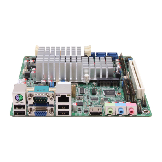
Page 7: Layout Diagram
Layout Diagram For 910 GMLE Gigabit LAN Line-OUT PS/2 Mouse PS/2 Keyboard MIC-IN Line-IN ATX Power Connector PS/2 Mouse Keyboard Intel 910 GMLE Express Chipset SFAN2 COM/VGA Connector LVDS Connector RJ45 LAN Intel LVDS Inverter. Over USB Port SFAN1 l USB 2.0 Port CPU FAN USB 2.0 Port ATA100... - Page 8 200-pin DDRII SODIMM NOTE! We strongly suggest there be a gap of at lease 5mm height reserved between this IPC board and the button of the chassis for the space needed to install a DDRII SODIMM at the back of the board.
- Page 9 Jumper Jumper Name Description Page Clear CMOS Function Setting 3-pin Block KB/USB Power On Function Setting 3-pin Block USB1/2 Power On Function Setting 3-pin Block LVDS Inverter Power On Setting 3-pin Block LVDS 5V/3.3 V Select 3-pin Block Connectors Connector Name Description Page...
-
Page 10: Checking Motherboard's Jumper Setting
Chapter 2 Jumper Setting, Connector & Header Checking Motherboard’s Jumper Setting (1) CMOS RAM Clear (3-pin): JP2 2-3 closed Clear CMOS 1-2 closed Normal (Default) CMOS Clear Setting (2) USB Power On function Enabled/Disabled (3-pin): JP3 When setting Enabled you can use USB Device to power on system. 1-2 closed KB/USB Power On Disabled (Default) 2-3 closed... -
Page 11: Connectors
(4) LVDS Inverter Function setting (3-pin): JP5 1-2 closed :Inverter Black Lighters On 2-3 closed: Inverter Black Lighters Off LVDS Inverter Function Setting (5) LVDS Function setting (3-pin): JP6 1-2 closed: LCD Powered by 5V 2-3 closed : LCD powered by 3.3V LVDS Function Setting Connectors Power Connector (20-pin block): ATXPWR1... - Page 12 (3) Primary IDE Connector (40-pin block): IDE1 IDE1 Pin 1 • Two hard disks can be connected to each connector. The first HDD is referred to as the “Master” and the second HDD is referred to as the “Slave”. • For performance issues, we strongly suggest you don’t install a CD-ROM or DVD-ROM drive on the same IDE channel as a hard disk.
-
Page 13: Headers
2-3 Headers (1) Line-Out, MIC-In Header (9-pin): AUDIO This header connects to Front Panel Line-out, MIC-In connector with cable. AUDIO Pin 1 Line-Out, MIC Headers (2) CD Audio-In Headers (4-pin): CDIN CDIN are the connectors for CD-Audio Input signal. Please connect it to CD-ROM CD-Audio output connector. - Page 14 (4) Serial Port Connector (9-pin female): COM2 COM2 is a 9-pin RS232 D-Subminiature serial port connector. Pin1 Pin6 Serial COM Port 9-pin Block (5) Speaker connector: SPEAK This 4-pin connector connects to the case-mounted speaker. See the figure below. (6) Power LED: PWR LED The Power LED is light on while the system power is on.
- Page 15 SFAN2 SFAN1 CPUFAN (11) SPDIF Out header: SPDIF SPDIF_OUT SPDIF_OUT (12) LVDS Pin-Headers: LVDS PIN No. Symbol PIN NO. Symbol These Headers can connect with the LVDS devices. CK2IN- CK2IN+ R2IN2- R2IN2+ R2IN1- R2IN1+ R2IN0- R2IN0+ LVDS_DDC_DATA LVDS_DDC-CLK CK1IN+ CK1IN- R1IN2+ R1IN2- R1IN1+...
-
Page 16: Chapter 3 Introducing Bios
(13) Pin-headers of LVDS Inverter: Inverter Panel Backlight Control LVDS Inverter Panel Backlight Enable Pin 1 Pin 2 (14) Expansion Daughter Board Headers: CN1/CN2 Press Down Directly To install a daughter board into CN1, CN2 is very easy, user just press down the daughter board directly into these two connectors, in the direction shown as the above picture. -
Page 17: Entering Setup
• Press Page Up/Page Down or +/– keys when you want to modify the BIOS parameters for the active option. Entering Setup Power on the computer and by pressing <Del> immediately allows you to enter Setup. If the message disappears before your respond and you still wish to enter Setup, restart the system to try again by turning it OFF then ON or pressing the “RESET”... - Page 18 Advanced BIOS Features Use this menu to set the Advanced Features available on your system. Advanced Chipset Features Use this menu to change the values in the chipset registers and optimize your system’s performance. Integrated Peripherals Use this menu to specify your settings for integrated peripherals. Power Management Setup Use this menu to specify your settings for power management.
-
Page 19: Standard Cmos Features
Standard CMOS Features The items in Standard CMOS Setup Menu are divided into several categories. Each category includes no, one or more than one setup items. Use the arrow keys to highlight the item and then use the <PgUp> or <PgDn> keys to select the value you want in each item. Phoenix –... -
Page 20: Advanced Bios Features
Advanced BIOS Features Phoenix – AwardBIOS CMOS Setup Utility Advanced BIOS Features Virus Warning Disabled Item Help CPU Feature Press Enter Hard Disk Boot Priority Press Enter Quick Power On Self Test Enabled Menu Level > First Boot Device Hard Disk Second Boot Device CDROM Third Boot Device... - Page 21 On (default) Keypad is numeric keys. Keypad is arrow keys. Typematic Rate Setting Keystrokes repeat at a rate determined by the keyboard controller. When enabled, the typematic rate and typematic delay can be selected. The settings are: Enabled/Disabled. Typematic Rate (Chars/Sec) Sets the number of times a second to repeat a keystroke when you hold the key down.
-
Page 22: Advanced Chipset Features
Advanced Chipset Features The Advanced Chipset Features Setup option is used to change the values of the chipset registers. These registers control most of the system options in the computer. Phoenix – AwardBIOS CMOS Setup Utility Advanced Chipset Features DRAM Timing Selectable By SPD Item Help * SDRAM CAS Latency Time... -
Page 23: Integrated Peripherals
You can reserve this area of system memory for ISA adapter ROM. When this area is reserved, it cannot be cached. The user information of peripherals that need to use this area of system memory usually discusses their memory requirements. The settings are: Enabled and Disabled. -
Page 24: Onboard Device Function
IDE Primary Master/Slave UDMA Ultra DMA100 implementation is possible only if your IDE hard drive supports it and the operating environment includes a DMA driver (Windows 95 OSR2 or a third-party IDE bus master driver). If your hard drive and system software both support Ultra DMA 100 and Ultra DMA/66, select Auto to enable BIOS support. -
Page 25: Power Management Setup
Onboard Serial Port 1 / 2 Select an address and corresponding interrupt for the serial ports. The optional settings are: 3F8/IRQ4, 2F8/IRQ3, 3E8/IRQ4, 2E8/IRQ3, 4E8/IRQ4,4E8/IRQ3,Disabled, and Auto. UART 2 Mold Select The optional settings are Normal and IRDA. Power Management Setup The Power Management Setup allows you to configure your system to most effectively save energy saving while operating in a manner consistent with your own style of computer use. -
Page 26: Pnp/Pci Configuration Setup
You can choose which month the system will boot up. Set to 0, to boot every day. Time(hh:mm:ss) Alarm You can choose what hour, minute and second the system will boot up. Note:If you have change the setting, you must let the system boot up until it goes to the operating system, before this function will work PnP/PCI Configuration Setup This section describes configuring the PCI bus system. -
Page 27: Smart Fan Configurations
Shutdown Temperature The optional settings are: Disabled, 60°C/140°F,65°C/149°F,70°C/158°F. Vcc 3V/ Vcore/+1.05V/+5V/+12V/5VSB/ VDIMM/ VSB3V/CPU Temperature /System Temperature/ CPU FAN Speed These are to show the current voltage of relative items, CPU/system temperature and current CPU fan speed. 3-10-1 Smart Fan Configurations Phoenix –... -
Page 28: Load Standard/Optimized Defaults
Users can select from a category of 1.1484V ~ 2.1563V. VRAM Select Users can select from a category of 1.8000V(Default )~2.5000V. Flash Part Write Protect The optional settings are Enabled and Disabled. 3-12 Load Standard/Optimized Defaults Load Standard Defaults When you press <Enter> on this item, you get confirmation dialog box with a message similar Load Standard Defaults (Y/N)? N Pressing <Y>...