Table of Contents
Advertisement
Quick Links
SERVICE MANUAL
Ver. 1.0 2013.01
SPECIFICATIONS
Frequency range
DAB (Band-III): 174. 928 MHz
239 .200 MHz
FM: 87.5 MHz
108 MHz (0.05 MHz step)
Intermediate frequency
DAB (Band-III): 2. 048 MHz
FM: 1.943 MHz
DAB (Band-III) frequency table (MHz)
Channel
Frequency
Channel
Frequency
5A
174.928
8C
5B
176.640
8D
5C
178.352
9A
5D
180.064
9B
6A
181.936
9C
6B
183.648
9D
6C
185.360
10A
6D
187.072
10N
7A
188.928
10B
7B
190.640
10C
7C
192.352
10D
7D
194.064
11A
8A
195.936
11N
8B
197.648
11B
Approx . 6.6 cm dia., 8 Ω, monaural
Speaker:
Audio power output:
0 .3 W
Output:
(headphones) jack (ø 3.5 mm, stereo mini jack)
Power requirements:
6 V DC, four LR6 (size AA) alkaline batteries
External power source:
DC IN 6 V
Battery life (JEITA)*:
Approx . 13 hours for DAB, 10 hours for FM (Using Sony (LR6SG) alkaline batteries)
Approx . 11 hours for DAB, 9 hours for FM (Using Sony (NH-AA) Ni-MH batteries)
Dimensions:
Approx . 180 mm × 95 mm × 36 mm (W/H/D) excl. projecting parts and controls
Mass:
Approx . 445 g incl. batteries
Supplied accessories:
AC adaptor (1)
* When listening through the speaker. Measured by JEITA (Japan Electronics and Information Technology
Industries Association) standards. The actual battery life may va ry depending on usage and circumstances.
Design and specifications are subject to change without notice.
9-893-659-01
Sony Corporation
2013A33-1
©
2013.01
Published by Sony Techno Create Corporation
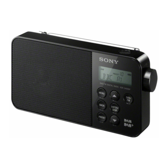
XDR-S40DBP
Channel
Frequency
199.360
11C
220.352
201.072
11D
222.064
202.928
12A
223.936
204.640
12N
224.096
206.352
12B
225.648
208.064
12C
227.360
209.936
12D
229.072
210.096
13A
230.784
211.648
13B
232.496
213.360
13C
234.208
215.072
13D
235.776
216.928
13E
237.488
217.088
13F
239.200
218.640
Operate the unit only on the power sources specified in "Specific ations. " For battery oper ation,
use four LR6 (size AA) alkaline batteries. For AC operation, use only the supplied AC adaptor.
Do not use any other type of AC adaptor.
Failure to use the supplied AC adaptor may cause the unit to malfunction, as
the polarity of the plugs of other manufacturers may be different.
When operating the unit on batteries, it is recommended that you remove the AC adaptor from
the wall outlet and the DC IN 6 V jack. Disconnect the plug of the external power source before
operating the unit.
NOTES ON CHIP COMPONENT REPLACEMENT
•
Never reuse a disconnected chip component.
•
Notice that the minus side of a tantalum capacitor may be dam-
aged by heat.
SAFETY-RELATED COMPONENT WARNING!
COMPONENTS IDENTIFIED BY MARK 0 OR DOTTED LINE
WITH MARK 0 ON THE SCHEMATIC DIAGRAMS AND IN
THE PARTS LIST ARE CRITICAL TO SAFE OPERATION.
REPLACE
THESE
COMPONENTS
WHOSE PART NUMBERS APPEAR AS SHOWN IN THIS
MANUAL OR IN SUPPLEMENTS PUBLISHED BY SONY.
DIGITAL RADIO DAB/FM
AEP Model
UK Model
Australian Model
WITH
SONY
PARTS
Advertisement
Table of Contents

Related Manuals for Sony XDR-S40DBP


Summary of Contents for Sony XDR-S40DBP
- Page 1 MANUAL OR IN SUPPLEMENTS PUBLISHED BY SONY. Battery life (JEITA)*: Approx . 13 hours for DAB, 10 hours for FM (Using Sony (LR6SG) alkaline batteries) Approx . 11 hours for DAB, 9 hours for FM (Using Sony (NH-AA) Ni-MH batteries) Dimensions: Approx .
-
Page 2: Table Of Contents
XDR-S40DBP SECTION 1 SERVICING NOTES TABLE OF CONTENTS UNLEADED SOLDER Boards requiring use of unleaded solder are printed with the lead- free mark (LF) indicating the solder contains no lead. SERVICING NOTES ..........(Caution: Some printed circuit boards may not come printed with... -
Page 3: Disassembly
XDR-S40DBP SECTION 2 DISASSEMBLY • This set can be disassembled in the order shown below. 2-1. DISASSEMBLY FLOW 2-2. CABINET REAR BLOCK 2-3. VOL KNOB BLOCK (Page 4) (Page 4) 2-4. CABINET FRONT ASSY (CAB1) (Page 5) 2-6. JACK BOARD 2-5. -
Page 4: Cabinet Rear Block
XDR-S40DBP Note: Follow the disassembly procedure in the numerical order given. 2-2. CABINET REAR BLOCK Note 1: Before removing the cabinet rear block, remove the always telescopic antenna (ANT1). Note 2: When installing the telescopic antenna (ANT1), install it on after installing the cabinet rear block. -
Page 5: Cabinet Front Assy (Cab1)
XDR-S40DBP 2-4. CABINET FRONT ASSY (CAB1) 1 tape 3 tapping screw JACK board 2 Remove solder. (B2.6) 2 Remove solder. (white) (red) Note: Wire must not run a ground into the solder portion of J201. tape [red] [white] 3 tapping screw (B2.6) -
Page 6: Lcddab Board
XDR-S40DBP 2-5. LCDDAB BOARD 1 two craws 1 two craws – – 2 Remove the LCDDAB board in the direction of an arrow. 4 LCDDAB board 3 Remove twelve solders. Note: Arrange a wire in order of arrow A and arrow B. -
Page 7: Jack Board
XDR-S40DBP 2-6. JACK BOARD Battery terminal setting Note 1: Insert only 1 turn in the ditch. battery terminal (minus) battery terminal (plus) chassis 4 battery terminal (plus) 2 battery terminal (minus) 6 screw 1 Remove solder. qs JACK board 5 Remove twelve solders. -
Page 8: Main Board Block
XDR-S40DBP 2-7. MAIN BOARD BLOCK 3 boss 1 screw 4 rib 2 claw 1 screw 4 rib 2 claw 3 boss – – 6 Remove twelve solders. 7 MAIN board block 5 Remove the MAIN board block in the direction of an arrow. -
Page 9: Main Board
XDR-S40DBP 2-8. MAIN BOARD 1 Remove the solder. 2 terminal 1 Remove the solder. (module) module assy (DAB module) 2 terminal (module) (DAB1) 1 Remove the solder. solder terminal (module) 2 terminal (module) 4 DAB module block 1.5 mm 1 Remove the solder. -
Page 10: Test Mode
XDR-S40DBP SECTION 3 TEST MODE 1. PREPARATION OF TEST MODE 3. VERSION, RTC AND CURRENT CONSUMPTION Prepare the following before checking test mode. CHECK • AC adaptor • Regulated DC power supply Procedure: • Dry battery 4PCS. (SIZE “AA”, IEC designation LR6) 1. - Page 11 XDR-S40DBP 4. FM RECEPTION CHECK 17. L channel is outputted from the signal generator, and L-chan- nel waveform is checked with an oscilloscope. Example: Procedure: 1. Input the following signal from signal generator to FM antenna input. L-ch Output frequency: 87.5 MHz...
- Page 12 XDR-S40DBP 5. DAB RECEPTION CHECK 6. INITIALIZE After the completion of repair, execute initialization. Procedure: All the settings, presets and the list of receivable DAB stations will 1. Input the following signal from signal generator to DAB an- be deleted.
-
Page 13: Diagrams
XDR-S40DBP SECTION 4 DIAGRAMS THIS NOTE IS COMMON FOR PRINTED WIRING BOARDS AND SCHEMATIC DIAGRAMS. • IC Block Diagrams (In addition to this, the necessary note is printed in each block.) – MAIN Board – For Schematic Diagrams. For Printed Wiring Boards. -
Page 14: Printed Wiring Board - Main Board
XDR-S40DBP 4-1. PRINTED WIRING BOARD - MAIN Board - • : Uses unleaded solder. MAIN BOARD CL101 S101 CN102 JL106 D103 JL110 CN104 D104 JL109 JL103 JL104 JL105 C128 ANT1 DAB1 TELESCOPIC MODULE ASSY R141 C144 R130 CL110 ANTENNA SL102... -
Page 15: Schematic Diagram - Main Board
XDR-S40DBP 4-2. SCHEMATIC DIAGRAM - MAIN Board - • See page 13 for IC Block Diagrams. MAIN BOARD CN101 CL107 W102 1.2V CL105 LCD_ON LCD_ON 3.3V KEYADIN KEYADIN C126 C127 C129 C132 LCD_RS 0.01 1000 0.01 1000 6.3V 6.3V KEYINT... -
Page 16: Printed Wiring Board - Jack Board
XDR-S40DBP 4-3. PRINTED WIRING BOARD - JACK Board - • : Uses unleaded solder. JACK BOARD CL205 CL206 CL203 SL203 CL202 CL201 CAB1 SL202 CABINET SL201 FRONT ASSY RV201 CL207 R226 R229 JW212 CL208 – VOL + C241 C240 JW213... -
Page 17: Schematic Diagram - Jack Board
XDR-S40DBP 4-4. SCHEMATIC DIAGRAM - JACK Board - JACK BOARD IC203 +3V REGULATOR Q202 IC203 F201 SSM3J305T (T5LSOY,E XC6201P302PR D207 TOTAL CURRENT FM: 134mA DB2J31600L JL201 DAB: 125mA R206 R207 R209 C208 C218 C219 DRY BATTERY 470k 470k SIZE "AA"... -
Page 18: Schematic Diagram - Lcddab Board
XDR-S40DBP 4-5. SCHEMATIC DIAGRAM - LCDDAB Board - • See page 13 for IC Block Diagrams. LCDDAB BOARD R315 R316 R317 Q304 W301 SSM3J15FU (T5LSOY, E LCD_ON KEYADIN LCD_RS R301 R304 KEYINY R319 LIGHT R305 LCD_A0 R361 R326 LCD_CS MAIN... -
Page 19: Printed Wiring Board - Lcddab Board
XDR-S40DBP 4-6. PRINTED WIRING BOARD - LCDDAB Board - • : Uses unleaded solder. LCDDAB BOARD (SHIELD CASE) C308 R319 Q305 R326 R361 R306 C307 D301 R305 IC301 R360 R304 BACK Q302 LIGHT LCD1 LIQUID CRYSTAL DISPLAY W301 JL347 JW301... -
Page 20: Exploded Views
XDR-S40DBP SECTION 5 EXPLODED VIEWS Note: • -XX and -X mean standardized parts, so • Color Indication of Appearance Parts Ex- they may have some difference from the ample: original one. KNOB, BALANCE (WHITE) . . . (RED) ... -
Page 21: Rear Cabinet Section
XDR-S40DBP 5-2. REAR CABINET SECTION • Rear side view Ref. No. Part No. Description Remark Ref. No. Part No. Description Remark 4-437-686-04 LID, BATTERY CASE (for BLACK) 4-459-425-01 CUSHION (BATTERY CASE LID A) (for BLACK) 4-437-686-24 LID, BATTERY CASE (for WHITE, RED) -
Page 22: Chassis Section
XDR-S40DBP 5-3. CHASSIS SECTION • Rear side view not supplied (MAIN board) CN104 DAB1 not supplied not supplied not supplied supplied J202 CAB1 not supplied (JACK board) not supplied LCDDAB board section Ref. No. Part No. Description Remark Ref. No. -
Page 23: Lcddab Board Section
XDR-S40DBP 5-4. LCDDAB BOARD SECTION not supplied (LCDDAB board) D301 LCD1 Ref. No. Part No. Description Remark Ref. No. Part No. Description Remark 4-437-728-01 CASE (LCD, DAB), SHIELD 4-437-691-01 LCD HOLDER (DAB) 4-437-733-01 SHEET, DIFFUSION 4-450-048-01 CUSHION (LIGHT GUIDE PLATE) -
Page 24: Electrical Parts List
XDR-S40DBP SECTION 6 JACK ELECTRICAL PARTS LIST Note: • Due to standardization, replacements in • CAPACITORS When indicating parts by reference num- the parts list may be different from the uF: μF ber, please include the board name. parts specifi ed in the diagrams or the com- •... - Page 25 XDR-S40DBP JACK LCDDAB MAIN Ref. No. Part No. Description Remark Ref. No. Part No. Description Remark R260 1-216-853-11 METAL CHIP 470K 1/10W R360 1-216-849-11 METAL CHIP 220K 1/10W R261 1-216-833-11 METAL CHIP 1/10W R361 1-216-845-11 METAL CHIP 100K 1/10W R262...
- Page 26 XDR-S40DBP MAIN Ref. No. Part No. Description Remark Ref. No. Part No. Description Remark < DIODE > < VARISTOR > D102 6-502-961-01 DIODE DA2J10100L VDR101 1-802-255-11 ESD SUPPRESSOR D103 6-502-961-01 DIODE DA2J10100L ************************************************************* D104 6-502-961-01 DIODE DA2J10100L D105 6-503-716-01 DIODE DB2J31600L...
- Page 27 XDR-S40DBP MEMO...
- Page 28 XDR-S40DBP REVISION HISTORY Checking the version allows you to jump to the revised page. Also, clicking the version at the top of the revised page allows you to jump to the next revised page. Ver. Date Description of Revision 2013.01...