Table of Contents
Advertisement
Quick Links
Oct.2001
SPECIFICATIONS.....................................................................................2
LOCATION OF CONTROLS ..................................................................4
LOCATION OF CONTROLS PARTS LIST ...........................................5
EXPLODED VIEW ....................................................................................6
EXPLODED VIEW PARTS LIST .............................................................7
PARTS LIST................................................................................................8
CHECKING THE VERSION NUMBER...............................................14
USERS DATA SAVE AND LOAD........................................................14
RESTORING THE FACTORY SETTINGS...........................................15
SYSTEM SOFTWARE UPDATE PROCEDURE..................................16
Updating by SMF ....................................................................................16
TEST MODE.............................................................................................17
BLOCK DIAGRAM.................................................................................22
Copyright © 2001 ROLAND CORPORATION
All rights reserved. No part of this publication may be reproduced in any form without the written permission
of ROLAND CORPORATION.
CIRCUIT BOARD (MAIN BOARD ASSY) ..........................................24
CIRCUIT BOARD (MAIN BOARD ASSY) ..........................................26
CIRCUIT BOARD (MAIN BOARD ASSY) ..........................................28
CIRCUIT BOARD (MAIN BOARD ASSY) ..........................................30
CIRCUIT BOARD (SW SHEET ASSY) .................................................32
CIRCUIT BOARD (SW SHEET ASSY) .................................................34
CIRCUIT DIAGRAM (MAIN BOARD ASSY/DIGITAL 1) ..............36
CIRCUIT DIAGRAM (MAIN BOARD ASSY/DIGITAL 2) ..............38
CIRCUIT DIAGRAM (MAIN BOARD ASSY/ANALOG)................40
CIRCUIT DIAGRAM (MAIN BOARD ASSY/POWER) ...................42
CIRCUIT DIAGRAM (SW SHEET ASSY) ..........................................44
ERROR MESSAGES ................................................................................46
17058021E0
SERVICE NOTES
Issued by RJA
Printed in Japan (0830) (AS)
SP-505
Advertisement
Table of Contents

Related Manuals for Roland SP-505


Summary of Contents for Roland SP-505
-
Page 1: Table Of Contents
CIRCUIT DIAGRAM (SW SHEET ASSY) ..........44 TEST MODE.....................17 ERROR MESSAGES ................46 BLOCK DIAGRAM.................22 Copyright © 2001 ROLAND CORPORATION All rights reserved. No part of this publication may be reproduced in any form without the written permission of ROLAND CORPORATION. 17058021E0... -
Page 2: Specifications
Oct.2001 SPECIFICATIONS Display 128 x 64 pixels Graphic LCD with backlight SP-505: Groove Sampling Connectors Workstation PHONES jack (Stereo 1/4 inch phone type) MIC jack (1/4 inch phone type) Maximum Polyphony LINE OUT jacks L/R (RCA phono type) LINE IN jacks L/R (RCA phono type) - Page 3 SP-505...
-
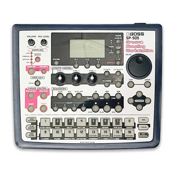
Page 4: Location Of Controls
Oct.2001 LOCATION OF CONTROLS fig.panel... -
Page 5: Location Of Controls Parts List
SP-505 LOCATION OF CONTROLS PARTS LIST PART CODE PART NAME DESCRIPTION Q’TY 22365714 CORD HOOK 13449728 ADAPTOR JACK HEC0740-010010 12499175 G S-BUTTON S1H BLK 249-175 00569278 6.5MM JACK LGR4609-7100 13429676 MIDI CONNECTOR YKF51-5048 (TWIN) 02236990 IC (OPTICAL CONNECTOR) GP1F550RZ RX... -
Page 6: Exploded View
Oct.2001 EXPLODED VIEW fig.explo... -
Page 7: Exploded View Parts List
SP-505 EXPLODED VIEW PARTS LIST [Parts] PART CODE PART NAME DESCRIPTION Q’TY 22365714 CORD HOOK 40344445 LABEL FCC CAUTION 02454523 BOTTOM COVER 02780878 LEAF SPRING 3 71788201 MAIN BOARD ASSY WITHOUT SPRING 02458301 WIRING1 (LCD BACKLIGHT) 02565034 F-51320GNY-LY-AA 02891134 LEAF... -
Page 8: Parts List
Oct.2001 PARTS LIST fig.part1e CONSIDERATION ON PARTS ORDRING SAFETY PRECAUTIONS: When ordering any parts listed in the parts list, please specify the following items in the order sheet. The parts marked have PART NUMBER DESCRIPTION MODEL NUMBER safety-related characteristics. Use 22575241 Sharp Key C-20/50... - Page 9 SP-505 02563089 NN51V4400BLTT-60 IC (DRAM) IC52 on MAIN 02781990 LH28F800BJE-PBTL90 IC (FLASH MEMORY) IC36 on MAIN ********** MBM30LV0064-PFTN-FJ IC (FLASH MEMORY) IC29 on MAIN 01780112 AK4522VF IC (AD/DA) IC6 on MAIN 00785245 TC75H00F(TE85L) IC (CMOS) IC64 on MAIN 02892334 IC (CMOS)
- Page 10 Oct.2001 RESISTOR 15399421 RPC10T 103 J 1/10W MTL.FILM RESISTOR R145,R46,R114,R88,R116,R128,R110,R144,R 77,R89,R174,R98,R105,R106,R153,R107,R12 9,R37,R60,R52,R181,R71,R176,R111,R75,R61 ,R76,R35,R34,R14,R11,R10,R4,R109,R73,R18 2,R179,R166,R165,R188,R187,R186,R185,R1 84,R183,R154,R160,R169,R161,R180,R156,R 155,R178,R108,R164 on MAIN R145 on SW 15399445 RPC10T 104 J 1/10W MTL.FILM RESISTOR R32,R33,R103,R1,R21,R139,R100,R140,R102, R95,R157,R158 on MAIN 15399469 RPC10T 105 J 1/10W MTL.FILM RESISTOR R3,R7,R13,R26,R87,R101 on MAIN 15399413 RPC10T 472 J 1/10W MTL.FILM RESISTOR...
- Page 11 SP-505 CAPACITOR 15359206 ECJ2VF1E104Z 100000PF/25V CERAMIC CAPACITOR C163,C135,C179,C177,C175,C174,C173,C17 1,C167,C166,C182,C164,C183,C162,C157,C1 55,C153,C152,C148,C147,C144,C143,C140,C 139,C138,C306,C165,C218,C305,C304,C303, C300,C232,C231,C230,C228,C227,C226,C18 0,C219,C130,C213,C212,C210,C208,C206,C2 05,C189,C188,C187,C186,C185,C184,C223,C 58,C137,C77,C74,C72,C69,C68,C65,C64,C63 ,C62,C81,C60,C82,C57,C56,C55,C53,C40,C2 9,C27,C25,C23,C22,C16,C12,C11,C61,C101, C129,C121,C116,C115,C114,C113,C110,C10 9,C108,C107,C104,C80,C102,C209,C99,C98, C97,C96,C94,C92,C90,C89,C87,C86,C85,C84 ,C83,C103,C207 on MAIN,C166,C167 on SW 15359440 ECJ2VB1H222K CERAMIC CAPACITOR C19,C14 on MAIN 00568456 ECJ1VF1C474Z CERAMIC CAPACITOR C67 on MAIN 01902590...
- Page 12 Oct.2001 SCREW 40011312 SCREW 3X8 BINDING TAPTITE P BZC 40015956 SCREW M3X12 BINDING HEAD S-TIGHT BZC 40235189 RING SE-9 PACKING 02789056 PAD ADAPTOR 02454623 PAD L 02454634 PAD R 02454612 PACKING CASE 02673589 OUTER PACKING CASE MISCELLANEOUS 40122645 NITTO FILAMENT TAPE #3883 W19MM 50M 60P (CM) 22365714 CORD HOOK...
- Page 13 SP-505...
-
Page 14: Checking The Version Number
Please format the card. Press [F1] (SAMPLE). Each pad bank in the SP-505’s internal memory will be saved as one set. When you save the all data, please repeate the action 5 to 8. Use the VALUE dial to select the pad bank that you want to save. -
Page 15: Restoring The Factory Settings
Use the VALUE dial to select the number of the area that you want to load. One bank of the SP-505’s internal memory will be loaded as a set. Never turn off the power while the display indicates “Keep Power On!”... -
Page 16: System Software Update Procedure
Press [SYSTEM] to display the System screen. Notes fig.10-01a Do not turn off the SP-505 while updating. The contents of the flash ROM may be damaged and the SP-505 will stop functioning. In this case, update again using the following [Updating by SmartMedia] procedure below. -
Page 17: Test Mode
Save user area data on the SmartMedia by using [USERS DATA SAVE AND LOAD] in this service note. Connect MIDI OUT if the MIDI sequencer can playback SMF data and SP-505 MIDI IN by MIDI cable. 0. contents Turn on the power while pressing the [F1], [F2] and [F3] buttons. - Page 18 Performs all items of the test mode. Make sure that the SmartMedia with the preset data has a write-protect sticker To enter the test mode, turn the SP-505’s power on while pressing the [WAVE affixed. ZOOM IN] and [PAD BANK] keys.
- Page 19 SP-505 [5] ENCODER CHECK [8] PHONES CHECK Turn the encoder clockwise. Connect an oscilloscope to the PHONES jack so that the output waveform can be observed. When the knob is fully turned until the meter displayed on the LCD reaches MAX, “OK”...
- Page 20 Confirm that “Insert Card” is displayed, and insert a SmartMedia card with a write-protect sticker affixed into the memory card slot. Confirm that “Protected.” is displayed. Next, prepare a SmartMedia formatted with SP-505. Confirm that there is no write-protect sticker on the SmartMedia and insert it into the memory card slot.
- Page 21 SP-505...
-
Page 22: Block Diagram
Oct.2001 BLOCK DIAGRAM fig.block Mai n Board AC IN (BRC-*V ) REGULA TOR REGULA TOR REGULA TOR DRAM FLASH DRAM MEMORY (Work) (Progra m) (MR2) D/A Data A/D Data GATE ARREY MIDI OUT V850 NAND MI DI IN Flash (Wave) FOOT SW Xí... - Page 23 SP-505 fig.block MI C VR Board LIN E IN REC LEVEL VOLUME BNCD-S-P=1.25-K-14-120(GS:7) (P/No. 02784889) PHONES LINE OUT DIGITAL IN...
-
Page 24: Circuit Board (Main Board Assy)
Oct.2001 CIRCUIT BOARD (MAIN BOARD ASSY) 71788201 Up to Serial No. ZP239739... - Page 25 SP-505 View from component side...
-
Page 26: Circuit Board (Main Board Assy)
Oct.2001 CIRCUIT BOARD (MAIN BOARD ASSY) 71788201 Up to Serial No. ZP239739... - Page 27 SP-505 View from foil side...
-
Page 28: Circuit Board (Main Board Assy)
Oct.2001 CIRCUIT BOARD (MAIN BOARD ASSY) 71788201 From Serial No. ZP239740... - Page 29 SP-505 View from component side...
-
Page 30: Circuit Board (Main Board Assy)
Oct.2001 CIRCUIT BOARD (MAIN BOARD ASSY) 71788201 From Serial No. ZP239740... - Page 31 SP-505 View from foil side...
-
Page 32: Circuit Board (Sw Sheet Assy)
Oct.2001 CIRCUIT BOARD (SW SHEET ASSY) 71788212... - Page 33 SP-505 71788212 View from component side...
-
Page 34: Circuit Board (Sw Sheet Assy)
Oct.2001 CIRCUIT BOARD (SW SHEET ASSY) 71788212... - Page 35 SP-505 71788212 View from foil side...
-
Page 36: Circuit Diagram (Main Board Assy/Digital 1)
Oct.2001 CIRCUIT DIAGRAM (MAIN BOARD ASSY/DIGITAL 1) fig.digital1 D 3. 3 C107 D 3. 3 1SS302 D 3. 3 IC27 TC74VHC245F FOOT SW RA3 1 SW-8 SW-7 SW-6 SW-5 N2012Z601T02 SW-10 RA4 1 SW-9 LGR4609-7100 SW-2 SW-1 C300 C108 N2012Z601T02 IC54C N2012Z601T02 TC7W14F... - Page 37 SP-505 fig.digital1 D-IN-F2 D-IN-F2 D-IN-F1 D-IN-F1 D-IN-F0 D-IN-F0 SW SCAN D-IN-VF D-IN-VF D-IN-DO D-IN-DO D-IN-XSTR D-IN-XSTR D-IN-ERR D-IN-ERR D-IN-DI D-IN-DI D-IN-CE D-IN-CE EXBV8V470JV SCAN9 SCAN16 D-IN-CL D-IN-CL SCAN11 SCAN15 DIN-POW-ON DIN-POW-ON SCAN13 SCAN14 SCAN15 SCAN13 GA-DMA-REQ2 GA-DMA-REQ2 EXBV8V470JV SCAN16 SCAN12...
-
Page 38: Circuit Diagram (Main Board Assy/Digital 2)
Oct.2001 CIRCUIT DIAGRAM (MAIN BOARD ASSY/DIGITAL 2) fig.digital2 CONTROL[0-50] D[0-15] A[0-9] D 3. 3 D 3. 3 C304 IC65B CD_XRE TC7WH74FU IC65A D 3. 3 IC66 R179 TC7WH74FU TC74LCX244FT N2012Z601T02 C305 D 3. 3 SM_XWE SM_XRE SM_ALE SM_CLE IC56C R180 D-IN-F2 TC7W32F C223... - Page 39 SP-505 fig.digital2 IC58 AN78L05M C183 D 3. 3 10(ohm) 10/16 N2012Z601T02 N2012Z601T02 (N2012Z601T02) C225 47/6.3(OS) 0.001 C184 0.001 DIGITAL C226 C227 C182 C196 R178 RECEIVER D 3. 3 1.5k(K) C146 0.001 C156 0.001 220/16 (100/16) IC56A TC9246FP TC7W32F SM_CS LOCK...
-
Page 40: Circuit Diagram (Main Board Assy/Analog)
Oct.2001 CIRCUIT DIAGRAM (MAIN BOARD ASSY/ANALOG) fig.analog 0.01 100k MIC IN N2012Z601T02 C190 100p C2 10p 1SS352 N2012Z601T02 LGR4609-7100 10/16 IC1A 30dB UPC4570G N2012Z601T02 1SS352 2SK880GR C193 2SK880GR 1SS352 10/16 C191 C220 IC5A 100p UPC4570G 10/16 100k 2SK880GR LINE IN JK2A N2012Z601T02 C195... - Page 41 SP-505 fig.analog LINE C185 C186 C187 C188 N3216Z501T01 MIC IN C173 D 3. 3 C189 ML_SEL IC3C (0-3.3V) IC8C IC5C NJM2100M UPC4570G UPC4570G RN2307 RN2307 A+9V C5 10/16 RN1307 1SS352 C174 A+4. 5V R141 IC1C IC4C IC1B C181 N2012Z601T02 UPC4570G...
-
Page 42: Circuit Diagram (Main Board Assy/Power)
Oct.2001 CIRCUIT DIAGRAM (MAIN BOARD ASSY/POWER) fig.power 2SA1706S-AN R120 IC45 R121 NJM2360A R123 0.33 VIN- (1/2W) C154 470p N2012ZP121T POWER SW ADAPTOR JK DSS9ND31H223Q SW1A HEC0740-010010 SDKLA1-B C160 C229 1000/25 ERZV07V330 CS S1NB60-4101 SW1B SDKLA1-B... - Page 43 SP-505 fig.power DIGITAL +5V DIGITAL I/F,LED DIGITAL +3.3V ELC10D221E D 3. 3 IC44 UPC29M33T C149 C150 C151 R119 470p 470/6.3 470/6.3 C152 C153 3.6k(K) SB07-03N R122 1.2k(K) ANALOG CODEC,DIGITAL I/F IC47 IC48 AN7809F AN78N05F C159 C163 C161 C162 C164 C165...
-
Page 44: Circuit Diagram (Sw Sheet Assy)
Oct.2001 CIRCUIT DIAGRAM (SW SHEET ASSY) fig.sw 100kA*2 CN12 VR1A EVJY95FB6A15 VR1C EVJY95FB6A15 LEVEL -infinity<-->+15dB VR1B EVJY95FB6A15 50kA*2 VR2C C166 14FE-ST-VK-N EVJY15FB6A54 VR2A EVJY15FB6A54 IC49 M66310FP VOLUME VR2B EVJY15FB6A54 R145 Control EN1A EVEGB1F15 24B C168 D 3. 3 EN1B EVEGB1F15 24B EEVMC1C100R(10/16) CTRL1 CTRL2... - Page 45 SP-505 fig.sw R128 R158 LED31 LNJ208R8ARA LED2 LNJ208R8ARA Pad 2 Pad 5 R157 R143 LED30 LNJ208R8ARA LED17 LNJ208R8ARA Part 2 Pad 6 R142 LED16 LNJ208R8ARA EXT Source by way of R154 R135 LED27 LNJ208R8ARA LED9 LNJ208R8ARA Pad 10 Pad 8...
-
Page 46: Error Messages
Oct.2001 ERROR MESSAGES MIDI Buffer Full! Too many MIDI messages were received all at once, and the SP-505 was unable to process all of them. Sampling related >Reduce the amount of MIDI messages being transmitted to the SP-505. Memory Full! - Page 47 The format of the inserted memory card is a format that the SP-505 cannot use. NAND memory (IC29) error >The SP-505 is able to use only 8-128 MB Smart Media memory cards with a 3.3 V power supply. Please check DRAM the type of card you are using.
- Page 48 Oct.2001 Update Failed Loading of the preset data failed. Delete File The preset data deletion failed. Write File File write failed. Read File File read failed. Verify File File read and write check failed. Not Exist Preset Full/half-line test was executed before the preset data was loaded.