Table of Contents
Advertisement
Please use this manual with the original service manual mentioned on the page 3.
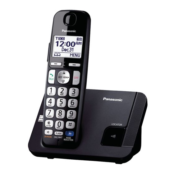
Telephone Equipment
Model No.
KX-TGE210B/KX-TGE212B/
KX-TGE232B/KX-TGE233B/
KX-TGE234B/KX-TGE240B/
KX-TGE242B/KX-TGE243B/
KX-TGE244B/KX-TGE245B/
KX-TGE262S/KX-TGE263S/
KX-TG454SK/KX-TGE272S/
KX-TGE273S/KX-TGE274S/
KX-TG484SK/KX-TGEA20B/
KX-TGEA20S
Digital Cordless Phone
Digital Cordless Answering System
Link-to-Cell Bluetooth Convergence
Solution
B: Black Version
S: Silver Version
T: Black Metallic Version
© Panasonic System Networks Co., Ltd. 2015
Unauthorized copying and distribution is a violation
of law.
ORDER NO. KM41512025SE
Advertisement
Table of Contents

Related Manuals for Panasonic KX-TGE210B


Summary of Contents for Panasonic KX-TGE210B
- Page 1 B: Black Version S: Silver Version T: Black Metallic Version Please use this manual with the original service manual mentioned on the page 3. © Panasonic System Networks Co., Ltd. 2015 Unauthorized copying and distribution is a violation of law.
-
Page 2: Table Of Contents
TABLE OF CONTENTS PAGE 1 ORIGINAL SERVICE MANUAL INFORMATION ----------3 2 REPLACEMENT PARTS LIST ---------------------------------3 2.1. REFERENCE CHART ------------------------------------3 2.2. ORIGINAL AND NEW PARTS COMPARISON LISTS----------------------------------------------------------4 3 CHANGES (Suffix Code: D or later) -------------------------5 3.1. Technical Descriptions ------------------------------------5 3.1.1. Block Diagram (Handset)----------------------------5 3.1.2. -
Page 3: Original Service Manual Information
1 ORIGINAL SERVICE MANUAL INFORMATION Suffix Code Model No. on S/M Destinations Order No. of S/M Base Unit Handset KX-TGE210B/KX-TGE212B/KX-TGE232B/KX-TGE233B/KX- U.S.A. KM41401789CE A to D TGE234B/KX-TGEA20B TGE240B, TGE242B, TGE243B, TGE244B, TGE245B: A to D TGE262S, TGE263S: KX-TGE240B/KX-TGE242B/KX-TGE243B/KX-TGE244B/KX- C to D TGE245B/KX-TGE260S/KX-TGE262S/KX-TGE263S/KX-TGE264S/ U.S.A. -
Page 4: Original And New Parts Comparison Lists
2.2. ORIGINAL AND NEW PARTS COMPARISON LISTS Serial No.Label tells you the suffix code as follows. (Example) Serial No. Label Suffix A Ref. No. Part No. Part Name & Description Pcs/ Remarks Notes Time of Change Original (Old) (Suffix) Cabinet and Electrical Parts (Handset) PNQT2859Z PNQT3384Z LABEL, BATTERY... -
Page 5: Changes (Suffix Code: D Or Later)
3 CHANGES (Suffix Code: D or later) 3.1. Technical Descriptions 3.1.1. Block Diagram (Handset) [Changed from original section “4.7. Block Diagram (Handset)”]... -
Page 6: Circuit Operation (Handset)
3.1.2. Circuit Operation (Handset) [Changed from original section “4.9. Circuit Operation (Handset)”] 3.1.2.1. Outline Handset consists of the following ICs as shown in Block Diagram (Handset) (P.5). • DECT BBIC (Base Band IC): IC1 - All data signals (forming/analyzing ACK or CMD signal) - All interfaces (ex: Key, Detector Circuit, Charge, DC/DC Converter, EEPROM, LCD, RF Power Amp.) - PLL Oscillator - Detector... -
Page 7: Test Mode
3.1.2.5. Speakerphone The hands-free loudspeaker at SP+ and SP- is used to generate the ring alarm. 3.2. Test Mode 3.2.1. Handset [Changed from original section “8.1.2. Handset”] Frequently Used Items (Handset) ex.) Items Address Default Data New Data Possible Adjusted Possible Adjusted Remarks Value MAX (hex) -
Page 8: Troubleshooting Guide
3.3. Troubleshooting Guide 3.3.1. Check Power 3.3.1.1. Handset [Changed from original section “10.1.1.2. Handset”] Is the battery inserted BATT+ and BATT-? (*1) Is the voltage of BATT+ 2.3 V more? Check F1 is not open. Check the battery and around BATT+ and BATT- are not shorted. -
Page 9: Check Link
3.3.2. Check Link 3.3.2.1. Handset [Changed from original section “10.1.5.2. Handset”] Does Handset make link with Base Unit? Handset is OK. Check Base Unit. (Correct working unit) (*1) Is the voltage of "1.8V" about 1.8 V? Adjust 1.8V voltage to 1.8 V. Check around Power Supply Circuit/Reset Circuit . -
Page 10: Check The Rf Part
3.3.3. Check the RF part [Changed from original section “10.1.6. Check the RF part”] Item BU (Base Unit) Check HS (Handset) Check Link Confirmation Normal 1. Register Regular HS to BU (to be 1. Register HS (to be checked) to Regular checked). -
Page 11: Disassembly And Assembly Instructions
3.4. Disassembly and Assembly Instructions 3.4.1. Handset [Changed from original section “11.1.2. Handset”] 2 screws Remove the 2 screws. Insert a plastic card. (Ex. Used SIM card etc.) Cabinet body between the cabinet body and the cabinet cover, then pull it along the gap to open the cabinet. -
Page 12: Measurements And Adjustments
3.5. Measurements and Adjustments 3.5.1. Adjustment Standard (Handset) [Changed from original section “12.4. Adjustment Standard (Handset)”] When connecting the simulator equipment for checking, please refer to below. 3.5.1.1. Component View ANT-Short ANT-Short-GND Green ANT1_TP Orange CP+3.0V 1.8V CP3V 1.8V P N L B 2 5 4 1 Z KX-TGEA20xx REF-2 15 H... -
Page 13: Things To Do After Replacing X'tal
3.5.2. Things to Do after Replacing X'tal 3.5.2.1. Handset [Changed from original section “12.5.1.2. Handset”] First, operate the PC setting according to The Setting Method of JIG. Then download the appropriate data according to the following procedures. Items How to download/Required adjustment FLASH(IC4) Adjusted parameter data is 1) Please be sure to execute the following steps if you have replaced the FLASH... -
Page 14: Miscellaneous
3.6. Miscellaneous 3.6.1. Terminal Guide of the ICs, Transistors and Diodes 3.6.1.1. Handset [Changed from original section “13.3.2. Handset”] Cathode (Reverse View) (Reverse View) Cathode 89 pin (GND) Anode B1ADGE000012, Anode B1ABGE000011, DSA900100L, 2SC6054JSL, PNWITGEA20RY UNR9216J0L C1CB00003837 B3ACB0000190 B3AFB0000370... -
Page 15: Schematic Diagram
3.7. Schematic Diagram 3.7.1. Schematic Diagram (Handset_Main) [Changed from original section “14.5. Schematic Diagram (Handset_Main)”] Charge Current VBAT To Battery VBAT BATT+_ ANT pattern BATT+ ANT-Short C120 K0.1u J68p BATT-_ SOCp BATT- ANT-Short-GND ANT1_TP J68p SOCn SHORT2 For Power Failure *Q10 *R10 Function... -
Page 16: Schematic Diagram (Handset_Module)
3.7.2. Schematic Diagram (Handset_Module) [Added to original section “14.6. Schematic Diagram (Hand_Module)”]... -
Page 17: Printed Circuit Board
3.8. Printed Circuit Board 3.8.1. Circuit Board (Handset_Main) [Changed from original section “15.3. Circuit Board (Handset_Main)”] 3.8.1.1. Component View CP4V Green Orange 1.8V CP3V P N L B 2 5 4 1 Z KX-TGEA20xx REF-2 CKM (10.368MHz) CHG (+) R500 for JIG GND/CHG (-) BATTERY... - Page 18 3.8.1.2. Bottom View REF-1 SOFT_A SOFT_C LEFT TALK RIGHT DOWN SHARP FLASH KX-TGE2xx CIRCUIT BOARD (Handset_Main (Bootom View))
-
Page 19: Circuit Board (Handset_Module)
3.8.2. Circuit Board (Handset_Module) [Added to original section “15.4. Circuit Board (Handset_Module)”] 3.8.2.1. Component View CP4V JTAG C190 C862 P N L B 2 4 3 1 Z * T G D A / T G K A 3 x R 0 KX-TGEA20 MODULE BOARD (Handset (Component View) 3.8.2.2. -
Page 20: Replacement Parts List
3.9. Replacement Parts List Safety Ref. Part No. Part Name & Description Remarks ECUE1H222KBQ 0.0022 3.9.1. Handset ECUE1H102KBQ 0.001 ECUV1C105KBV 1 3.9.1.1. Main P.C. Board Parts F1G0J1050007 1 ECUV1C105KBV 1 3.9.1.1.1. Main P.C. Board F1G1A1040006 0.1 C113 ECUE1H100DCQ 10p [Changed from original section “16.5.2.2. Main P.C. Board C120 ECUE1H680JCQ 68p Parts”]... - Page 21 Safety Ref. Part No. Part Name & Description Remarks ECUE1H100DCQ 10p ECUE1H100DCQ 10p F1G1A1040006 0.1 F1G0J1050007 1 F1G1A1040006 0.1 ECUE1H100DCQ 10p ECUE1H100DCQ 10p C190 F1G1A1040006 0.1 C191 F1G0J1050007 1 C859 ECUE1H100DCQ 10p C860 F1G1H1R2A765 1.2p C862 F1G1H1R5A765 1.5p C863 F1G1H1R8A798 1.8p C865 ECUE1H100DCQ 10p C866...