
Related Manuals for Panasonic SA-HT990E


Summary of Contents for Panasonic SA-HT990E
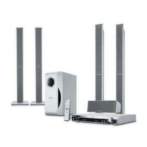
- Page 1 ORDER NO.MD0603064C2 DVD Home Theater Sound System SA-HT990E / SA-HT990EB / SA-HT990EG Colour (S).......Silver Type SPECIFICATIONS Specifications...
- Page 2 General Power Source: E/ EG areas: AC 230V, 50Hz EB area: AC 230V-240V, 50Hz Power consumption: 120 W Dimensions (W×H×D): 430×60×354 mm Mass: 3.35kg Amplifier section RMS Output Power: Dolby Digital Mode Total RMS Dolby 1000 W Digital mode Power: At 1kHz and total harmonic of 10% 125 W/ Channel (3 Front:...
- Page 3 4096 pixels (Sub sampling is 4:0:0, 4:2:0, 4:2:2, 4:4:4). Extremely long and narrow pictures may not be displayed. *4 MPEG4 data recorded with Panasonic SD multi cameras or DVD video recorders. Conforming to SD VIDEO specifications (ASF standard)/ MPEG4 (Simple Profile) video system/G.726 audio system.
- Page 4 DVD (linear audio): 95 dB CD-Audio: 95 dB Total harmonic distortion: CD-Audio: 0.005 % Video section Video system: Signal system: PAL 625/50, PAL 525/60, NTSC Composite video output: Output level: 1 Vp-p (75 Terminal: Pin jack (1 system) Scart jack (1 system) S-video output: Y output level: 1 Vp-p (75...
- Page 5 Refer to the original service manual for *1, *2, *3, *4. 2006 Panasonic AVC Networks Singapore Pte. Ltd. All rights reserved. Unauthorized copying and distribution is a violation of law.
-
Page 6: Safety Precautions
1. Safety Precautions 1.1. GENERAL GUIDELINES 1. When servicing, observe the original lead dress. If a short circuit is found, replace all parts which have been overheated or damaged by the short circuit. 2. After servicing, see to it that all the protective devices such as insulation barriers, insulation papers shields are properly installed. -
Page 7: Before Repair And Adjustment
1.1.2. LEAKAGE CURRENT HOT CHECK (See Figure 1. Plug the AC cord directly into the AC outlet. Do not use an isolation transformer for this check. 2. Connect a 1.5k , 10 watts resistor, in parallel with a 0.15 capacitors, between each exposed metallic part on the set and a good earth ground such as a water pipe, as shown in Figure 3. -
Page 8: Protection Circuitry
Current consumption at AC 220V-230 V, 220V/230V-240V, 50Hz in NO SIGNAL mode volume minimal should be ~ 600 mA (For EB). 1.3. Protection Circuitry The protection circuitry may have operated if either of the following conditions are noticed: - No sound is heard when the power is turned on. - Sound stops during a performance. -
Page 9: Precaution Of Laser Diode
can generate electrical charge sufficient to damage ES devices. 5. Do not use freon-propelled chemicals. These can generate electrical charges sufficient to damage ES devices. 6. Do not remove a replacement ES device from its protective package until immediately before you are ready to install it. (Most replacement ES devices are packaged with leads electrically shorted together by conductive foam, aluminum foil or comparable conductive material). -
Page 10: About Lead Free Solder (Pbf)
4. About Lead Free Solder (PbF) Distinction of PbF PCB: PCBs (manufactured) using lead free solder will have a PbF stamp on the PCB. Caution: - Pb free solder has a higher melting point than standard solder; Typically the melting point is 50 - 70°F (30 - 40°C) higher. Please use a high temperature soldering iron. -
Page 11: Handling Precautions For Traverse Unit
6. Handling Precautions for Traverse Unit The laser diode in the optical pickup unit may break down due to static electricity of clothes or human body. Special care must be taken avoid caution to electrostatic breakdown when servicing and handling the laser diode. 6.1. -
Page 12: Grounding For Electrostatic Breakdown Prevention
2. To prevent the laser diode from the electrostatic discharge damage, the flexible cable of the optical pickup unit removed should be short-circuited with a short pin or a clip. 3. The flexible cable may be cut off if an excessive force is applied to it. - Page 13 6.2.1. Worktable grounding 1. Put a conductive material (sheet) or iron sheet on the area where the optical pickup is placed, and ground the sheet. 6.2.2. Human body grounding 1. Use the anti-static wrist strap to discharge the static electricity form your body.
-
Page 14: Operation Procedures
AC cord / (For EB area) AC cord / (For E, EG areas) Speaker cable Video cable / (For E, EG areas) Speaker label 8. Operation Procedures 8.1. Remote Control Keys Operation... -
Page 15: About Divx Vod Content
8.2. Main Unit Keys Operation 8.3. Disc information 8.3.1. DISC playability (Media) 8.3.2. File Extension Type Support (WMA/JPEG/MP3) 8.4. About DivX VOD Content 9. Self-Diagnosis and special mode setting 9.1. Service Mode Summary Table The service modes can be activated by pressing various button combination on the player and remote control unit. -
Page 16: Service Mode Table
Player buttons Remote control unit Application Note buttons STOP Error code display (Refer to section, Self Diagnostic Function Code”). Jitter checking (Refer to section “ Service Table 1 for information”). Region display and mode (Refer to section “ Micro-processor firmware version check Service Table 1 for information”). -
Page 17: Dvd Self Diagnostic Function-Error Code
when the value of the laser drive current is more than 55. Note: Press the power button to turn on the power, and check the value within three minutes before the unit warms up. (Otherwise, the result will be incorrect.) 9.3. - Page 18 Description of error Automatic FL Display Remarks Error Diagnosis Contents Code Focus coil NG (OPU unit Press [ STOP] Focus servo error abnormal) on main unit for next error. Press [ STOP] Tray loading error / The tray is not able to open on main unit for abnormality next error...
- Page 19 Description of error Automatic FL Display Remarks Error Diagnosis Contents Code Press [ STOP] F504 Abnormal adjusting on main unit for DSC data slice next error offset Press [ STOP] F505 DSC Attention error Similar as F500 on main unit for next error Press [ STOP]...
- Page 20 Description of error Automatic FL Display Remarks Error Diagnosis Contents Code Press [ STOP] F700 MBX overflow When replying message to on main unit for disc manager next error Press [ STOP] F701 Message command Next message is sent before on main unit for does not end replying to disc manager...
-
Page 21: Sales Demonstration Lock Function
next error Note: An error code will be canceled if a power supply is turned OFF. *1: CPPM is the copy guard function beforehand written in the disk for protection of copyrights. *2: CEC is the consumer electronic control used for high-level user control of HDMI-connected devices. -
Page 22: Service Precautions
Player , SELECTOR, , VOLUME KNOB, DISC CHECK, DISC CHANGE, DISC1-DISC5 Remote controller SLEEP, REPEAT, 0~9, , RETURN, TOP MENU, unit , POSITION MEMORY, TUNER/BAND, D.MIX, CH SELECT/ TEST, SET UP/ MUTING, DISPLAY, GROUP, TV, VCR/ AUX, QUICK REPLAY, SUBTITLE, FL DISPLAY, CH &... -
Page 23: Assembling And Disassembling
updating is to be done or not. (Selection of Yes/No) 4. a. If Yes is selected, version updating is performed. b. If No is selected, only recovery is performed. 5. a. When updating is finished, remove the disc according to the message appearing on the screen. - Page 24 major printed circuit boards and main components. 2. Before the disassembly process was carried out, do take special note that all safety precautions are to be carried out. (Ensure that no AC power supply is connected during disassembling.) 3. For assembly after operation checks or replacement, reverse the respective procedures.
-
Page 25: Main Components And P.c.b. Locations
10.2. Main Components and P.C.B. Locations 10.3. Disassembly of Top Cabinet Step 1 Remove 4 screws. -
Page 26: Disassembly Of The Dvd Lid (When Taking Out Disc Manually)
Step 2 Remove 3 screws. (Rear view) Step 3 Lift up and remove the top cabinet. 10.4. Disassembly of the DVD Lid (When taking out disc manually) Step 1 Detach the gear for drawing out tray from the mechanism unit. It inserts a screw driver in the gear. -
Page 27: Disassembly Of Front Panel Assembly
10.5. Disassembly of Front Panel Assembly - Follow the Item 10.3. Step 1 Remove the DVD lid. Step 2 Detach FFC cables at connectors. (CN2006, CN2007) Step 3 Remove 1 screw. Step 4 Release the tabs. -
Page 28: Disassembly Of Music Port P.c.b, Fl P.c.b. & Top Button
Step 5 Detach the front panel assembly. Special Note: Avoid placing the set in a position that might cause damage to the jacks when removing the front panel assembly. 10.6. Disassembly of Music Port P.C.B, FL P.C.B. & Top Button P.C.B. -
Page 29: Disassembly Of Dvd Mechanism Unit
Step 7 Remove 6 screws. Step 8 Remove FL P.C.B. &/or Top Button P.C.B. 10.7. Disassembly of DVD Mechanism Unit - Follow the Item 10.3. - Follow (Step 1) of Item 10.5. Step 1 Remove 2 screws. Step 2 Detach FFC cables at connectors. (CN2004, CN2001). Step 3 Lift up the mechanism unit vertically to remove it. -
Page 30: Disassembly Of Rear Panel
Step 1 Remove 4 screws. Step 2 Detach FFC cables at the connectors.(FP8251, FP8531) Caution: Do not apply or exert excessive force when detaching the FFC cables. 10.9. Disassembly of Rear panel - Follow the Item 10.3. Step 1 Remove 9 screws. Step 2 Detach connector(CN5704) at fan unit. -
Page 31: Disassembly Of Main P.c.b
10.11. Disassembly of Main P.C.B. - Follow the Item 10.7. - Follow the (Step 1) of Item 10.10. Step 1 Remove 5 screws. Step 2 Lift up and remove Main P.C.B. 10.12. Disassembly of Digital Amp IC - Follow (Step 1) to (Step 2) of Item 10.11. Step 1 Desolder all IC5000, IC5200, IC5300 pins. - Page 32 10.13. Disassembly of Digital Amp IC (IC5400) - Follow (Step 1) to (Step 2) of Item 10.11. Step 1 Desolder all pins of IC5400. Step 2 Desolder 2 pins of Heat Sink B. Step 3 Remove the Digital Amp IC (IC5400). Note: Refer to the diagrams of Power P.C.B.
-
Page 33: Service Position
Step 2 Desolder 2 pins of Switch Regulator IC. Step 3 Remove the Switch Regulator IC. Note: Refer to the diagrams of Power P.C.B. (Section 19.2) for location of the parts. Caution: Be careful when removing the Switch Regulator IC which has high temperature after prolonged use. -
Page 34: Assembly And Disassembly Of Mechanism Unit
Step 2 Turn Main P.C.B to vertically position. 11. Assembly and disassembly of Mechanism Unit 11.1. Disassembly Procedure 11.1.1. Disassembly of Traverse Unit Step 1 Slide the lever (A) in the arrow direction (to the opposite side) till it stops. - Page 35 Step 2 Slide the lever (A) further by bending the tab at the right side of the lever A in the right direction. (The right groove opens and the boss becomes seen.) Step 3 Open the lever (B) to left. (The 2 grooves at the left side open.). Step 4 Remove the traverse unit.
- Page 36 Step 2 Raise the loading unit. Step 3 Slide the lever in the arrow direction till it stops and pull the tray out. Step 4 Spread the tabs at the both sides and pull the tray out. (The tray slides a little forword and stops.).
- Page 37 (Assembling the tray unit) Step 1 Insert a part of the tray into the unit sliding over the groove on the mechanical chassis unit. Step 2 Insert the tray to the point before the tab of the mechanical chassis unit. Step 3 Hook the drive arm concave phase over the tray and the tray slider.
- Page 38 11.1.3. Disassembly of Loading section Step 1 Spread the tabs at the both sides and push out the drive arm shaft. Step 2 Hook the lock lever spring on the lock lever projection part temporarly. Step 3 Unlock the tab and remove the lock lever.
- Page 39 Step 4 Remove the belt. Step 5 Unlock the tab and remove the pulley. Step 6 Remove the relay gear. Step 7 Turn the change lever in the arrow direction till it stops. Step 8 Hook the change lever spring on the change lever project part temporarily.
- Page 40 Step 9 Pull the lever (B) in the bottom side to your side and remove the change lever. Step 10 Remove the drive rack, the sub rack and the drive gear. 11.1.4. Disassembly of Tray Loading P.C.B. Step 1 Remove 3 screws...
- Page 41 11.1.5. Disassembly of Optical Pickup Unit Special Note: Anti-static measures are necessary due to handling of OPU unit . Step 1 Spread the tabs to push in the pin. Step 2 Remove 4 pins.
- Page 42 Step 3 Remove the middle chassis. Step 4 Remove the optical pickup unit in the arrow direction till it stops. Step 5 Remove 2 screws.
- Page 43 Step 6 Remove the drive rack. Step 7 Remove 1 screw. Step 8 Slide the shaft in the arrow direction. Step 9 Lift the optical pickup unit with the shaft.
- Page 44 Step 10 Remove the optical pickup unit. Step 11 Pull the shaft and the rubber out. (Assembling the optical pickup unit) Step 1 Pass the intermediate FPC through the frame hole. Step 2 Align the guide section of the optical pickup unit with the rail. Step 3 Install the shaft top to the holder.
-
Page 45: Measurements And Adjustments
12. Measurements and Adjustments 12.1. Service Tools and Equipment Application Name Number Tilt adjustment DVD test disc DVDT-S20 [SPG] TORX screw driver (T6) Available on sales route. (T6) or RFKZ0185 [SPG] Others Grease RFKXPG641 [SPG] Confirmation CD test disc PVCD-K06 or any other commercially available disc VCD test disc PVCD-K06 or any other... -
Page 46: Optical Adjustment
make adjustment if there is a noticeable degradation in picture quality. Optical adjustments cannot be made inside the optical pickup. Adjustment is generally unnecessary after replacing the traverse unit. 12.2.2. Important points in electrical adjustment - Follow the adjustment procedures described in this manual. 12.3. - Page 47 counter, while "zz" is the focus drive value. Note: Jitter value appears on the front display. 3. Play test disc T30 (center periphery). 4. Adjust tangential adjustment screw so that the jitter value is minimized. 5. Play test disc T30 (center periphery). 6.
- Page 48 12.4.1.3. Check after adjustment Play test disc or any other disc to make sure there is no picture degradation in the inner, middle and outer peripheries, and no audio skipping. After adjustment is finished, lock each adjustment screw in position using screw lock. 12.4.1.4.
- Page 49 12.5. Abbreviations INITIAL/LOGO ABBREVIATIONS A0~UP ADDRESS ACLK AUDIO CLOCK AD0~UP ADDRESS BUS ADATA AUDIO PES PACKET DATA ADDRESS LATCH ENABLE AMUTE AUDIO MUTE AREQ AUDIO PES PACKET REQUEST AUDIO RF SERVO AMP INVERTED INPUT SERVO AMP OUTPUT ASYNC AUDIO WORD DISTINCTION SYNC BIT CLOCK (PCM) BCKIN...
- Page 50 INITIAL/LOGO ABBREVIATIONS CONSTANT ANGULAR VELOCITY CBDO CAP. BLACK DROP OUT COMPACT DISC CDSCK CD SERIAL DATA CLOCK CDSRDATA CD SERIAL DATA CD RF (EFM) SIGNAL CDRF COMPACT DISC-VIDEO CHANNEL DATA CHNDATA SYSTEM CLOCK SELECT CKSL CONSTANT LINEAR VELOCITY CAP. OFF TRACK COFTR CPU ADDRESS CPU CHIP SELECT...
- Page 51 INITIAL/LOGO ABBREVIATIONS ERROR TORQUE CONTROL ERROR TORQUE CONTROL REFERENCE ENCODER SELECT ENCSEL EXTERNAL M CLOCK (81MHz/ ETMCLK 40.5MHz) ETSCLK EXTERNAL S CLOCK (54MHz) FBAL FOCUS BALANCE FCLK FRAME CLOCK FOCUS ERROR FOCUS ERROR AMP INVERTED INPUT FOCUS ERROR AMP OUTPUT FREQUENCY GENERATOR FREQUENCY SUB CARRIER FSCK...
- Page 52 INITIAL/LOGO ABBREVIATIONS MA0~UP MEMORY ADDRESS MEMORY CLOCK MCKI MEMORY CLOCK INPUT MCLK MEMORY SERIAL COMMAND CLOCK MDATA MEMORY SERIAL COMMAND MDQ0~UP DATA MDQM MEMORY DATA INPUT/OUTPUT MPEG MEMORY DATA I/O MASK MEMORY SERIAL COMMAND LOAD MOVING PICTURE EXPERTS GROUP OPTICAL DISC CONTROLLER OFTR OFF TRACKING OSCI...
- Page 53 INITIAL/LOGO ABBREVIATIONS READ ENABLE RFENV RF ENVELOPE RF PHASE DIFFERENCE OUTPUT (CD-ROM) REGISTER SELECT RSEL RF POLARITY SELECT RESET RESERVE SBI0, 1 SERIAL DATA INPUT SBO0 SERIAL DATA OUTPUT SBT0, 1 SERIAL CLOCK SERIAL DATA CLOCK SCKR AUDIO SERIAL CLOCK RECEIVER SERIAL CLOCK SCLK...
- Page 54 SUB CODE Q DATA SYSCLK SYSTEM CLOCK INITIAL/LOGO ABBREVIATIONS TRACKING ERROR TIBAL BALANCE CONTROL BALANCE OUTPUT 1 BALANCE INPUT BALANCE INPUT BALANCE OUTPUT 2 TPSN OP AMP INPUT TPSO OP AMP OUTPUT TPSP OP AMP INVERTED INPUT TRCRS TRACK CROSS SIGNAL TRON TRACKING ON TRSON...
-
Page 55: Voltage And Waveform Chart
INITIAL/LOGO ABBREVIATIONS X' TAL XALE X ADDRESS LATCH ENABLE XAREQ X AUDIO DATA REQUEST XCDROM X CD ROM CHIP SELECT X CHIP SELECT XCSYNC X COMPOSITE SYNC X DATA STROBE XHSYNCO X HORIZONTAL SYNC OUTPUT XHINT XH INTERRUPT REQUEST X' TAL OSCILLATOR INPUT XINT X INTERRUPT X MEMORY WRITE ENABLE... - Page 56 Play detection switch. S902: Open detection switch. S6800: Tray open / close switch ( Open / Close). S6805: R. skip, search and Tuning switch ( / TUNING S6801: Stop and TUNE mode /FM mode switch ( TUNE MODE/FM MODE). / S6802: Play and memory switch ( Memory).
-
Page 57: Schematic Diagram
When replacing any of components, be sure to use only manufacturer´s specified parts shown in the parts list. - The supply part number is described alone in the replacement parts list. - Voltage and signal line : +B Signal line : CD-DA signal line : Main signal line : DVD (Video) signal line... -
Page 58: Printed Circuit Board
18.2. (B) Main/Power Circuit 18.3. (C) FL, Music Port, Top Button, Tuner Extent and Tray Motor Circuit 18.4. (D) Scart Circuit 19. Printed Circuit Board 19.1. (A) DVD Module P.C.B. 19.2. (B) Main & Power P.C.B. 19.3. (C)Tuner extent, AC-inlet, FL, Music Port, & Top button P.C.B. 19.4. - Page 59 Terminal Name I/O Function 1 TRY_ / CLOSE I Loading mechanism close SW ( L: SW ON ) 2 TRAY_CCW O Terminal for tray control 1 3 TRAY_CW O Terminal for tray control 2 4 TRY_OPEN I Loading Mechanism open SW ( L: SW ON ) 5 MP_DAC1 - No connection...
- Page 60 Terminal Name I/O Function 31 RF_DET I RF module detection - wireless ready 32 RF_PCON - RF power control 33 RF_LINK I RF link control - wireless ready 34 RF_DATA O RF change direction - wireless ready 35 TUN_SD I CMD signal for the DVD Module 36 TUN_CLK O I2C Clock Data Tuner...
- Page 61 Terminal Name I/O Function 66 MIC_SW O Mic surround 67 HOP_DA O Digital Amp frequency hop control 68 MUTE_S O Mute signal for surround Audio signal 69 MUTE_F O Mute signal output for Front speaker 70 DC_DET I Signal from the DC Detection circuit 71 MOD_DA O Digital amplifier standby...
-
Page 62: Exploded Views
Terminal Name I/O Function 97 KEY1 I Key 1 line input 98 VREF - Reference voltage input 99 AVCC - Analog power supply input 100 BRAKE_H O Terminal for tray control 3 23. Exploded Views 23.1. Cabinet Parts Location... - Page 64 23.2. Packaging...
-
Page 65: Replacement Parts List
24. Replacement Parts List Notes: *Important safety notice: Components identified by mark have special characteristics important for safety purpose. Furthermore, special parts which have purposes of fire-retardant (resistors), high-quality sound (capacitors), low-noise (resistors), etc. are used. When replacing any of components, be sure to use only manufacture’s specified parts shown in the parts list. -
Page 66: Component Parts List
*Resistance values are in ohms, unless specified otherwise, 1K=1,000 (OHM), 1M=1,000K (OHM). *The parenthesized indications in the Remarks columns specify the model names and areas. (Refer to the cover page) *The marking (RTL) indicates the retention time is limited for this item. After the discontinuation of this assembly in production, it will no longer be available. - Page 67 Ref. No. Part No. Part Name & Description Remarks RXXX0070 HEAT SINK B XTB3+10JFJ SCREW XTW3+15TFJ SCREW REEX0506 19P FFC CABLE RMAX0086 PANEL ANGLE CASSETTE DECK TRAVERSE DECK RHM0003-J MAGNET RDG0547 PULLEY GEAR RDG0548-1 RELAY GEAR RDG0549 DRIVE GEAR RDV0070 BELT REM0102 MOTOR UNIT...
- Page 68 Ref. No. Part No. Part Name & Description Remarks INTEGRATED CIRCUITS IC904 C0GAY0000013 IC MOTOR DRIVER IC1101 C9ZB00000461 IC VIDEO BUFFER IC1102 C1AB00001731 IC VIDEO BUFFER IC2005 C1BB00001008 IC RDS IC2018 C2CBYY000195 IC MICRO-PROCESSOR IC2102 C1BB00001098 IC ASP IC2103 C0AABB000125 IC HEADPHONES AMP IC2104 C0ABCB000052...
- Page 69 Q2101 B1GFGCAA0001 TRANSISTOR...
- Page 70 Ref. No. Part No. Part Name & Description Remarks Q2201 B1GDCFGA0018 TRANSISTOR Q2303 B1GDCFGA0018 TRANSISTOR Q2304 B1ABCF000176 TRANSISTOR Q2305 B1GFGCAA0001 TRANSISTOR Q2306 B1GFGCAA0001 TRANSISTOR Q2801 B1GBCFJN0033 TRANSISTOR Q2804 B1GBCFJN0033 TRANSISTOR Q2805 B1GBCFJN0033 TRANSISTOR Q2903 B1BACD000018 TRANSISTOR Q2904 B1AAKD000012 TRANSISTOR Q2906 B1BCCG000002 TRANSISTOR Q2907...
- Page 71 DIODES...
- Page 72 Ref. No. Part No. Part Name & Description Remarks D2005 B0ACCK000005 DIODE D2007 B0ACCK000005 DIODE D2008 B0ACCK000005 DIODE D2600 B0ACCK000005 DIODE D2601 B0ACCK000005 DIODE D2603 B0ACCK000005 DIODE D2800 B0ACCK000005 DIODE D2902 B0BC7R500001 DIODE D2904 B0JCPD000025 DIODE D2906 B0ADCJ000020 DIODE D2907 B0ADCJ000020 DIODE D2915...
- Page 73 Ref. No. Part No. Part Name & Description Remarks D5749 B0EAMM000057 DIODE D5750 B0ACCK000005 DIODE D5752 B0BC5R000009 DIODE D5753 B0ACCK000005 DIODE D5754 B0ACCK000005 DIODE D5903 B0BC01200019 DIODE D5923 B0BC01200019 DIODE D6900 B3AAA0000803 DIODE D6910 B0BC4R3A0006 DIODE D8211 MA2J11100L DIODE D8571 MA2J72800L DIODE CHIP INDUCTORS...
- Page 74 Ref. No. Part No. Part Name & Description Remarks VARIABLE RESISTORS VR6800 EVEKE2F2524M VOLUME JOG SWITCHES S901 RSH1A044-1A SW PLAY S902 RSH1A044-1A SW OPEN S6800 EVQ21405R SW OPEN/CLOSE S6801 EVQ21405R SW STOP S6802 EVQ21405R SW PLAY S6803 EVQ21405R SW SELECTOR S6804 EVQ21405R SW FORWARD...
- Page 75 Ref. No. Part No. Part Name & Description Remarks L2009 G0C220JA0055 COIL L2700 J0JBC0000041 CHIP INDUCTOR L2701 J0JBC0000041 CHIP INDUCTOR L2703 J0JBC0000041 CHIP INDUCTOR L2801 G0C220JA0055 COIL L2802 J0JBC0000015 CHIP INDUCTOR L2803 J0JBC0000015 CHIP INDUCTOR L2804 J0JBC0000015 CHIP INDUCTOR L2805 J0JBC0000015 CHIP INDUCTOR L2806...
- Page 76 Ref. No. Part No. Part Name & Description Remarks OSCILLATORS X2001 H2B100500004 CERAMIC RESONATORS X2700 H0H433400002 CRYSTAL X5500 H2A375300003 CERAMIC RESISTOR X5501 H2A415300001 CERAMIC RESISTOR X8621 H0J270500085 CRYSTAL DISPLAY TUBE FL6901 A2BD00000160 FL DISPLAY FL8101 F1H0J1050022 CHIP CAPACITOR FL8102 F1H0J1050022 CHIP CAPACITOR FL8103 F1H0J1050022...
- Page 77 Ref. No. Part No. Part Name & Description Remarks RQT8601-D O/I BOOK (SP/PO/CZ) [M]EG RQT8602-H O/I BOOK (GE/IT/FR) [M]EG RQT8603-D O/I BOOK (DU/DA/SW) [M]E RQT8604-H O/I BOOK [M]E RSA0007-L FM ANTENNA N1DAAAA00002 AM LOOP ANTENNA K2KA2BA00001 VIDEO CABLE [M]EG/E REEX0449B-1L SPEAKER CORD RQCA0968 SPEAKER LABEL...
- Page 78 Ref. No. Part No. Part Name & Description Remarks R2014 ERJ3GEYJ273V 27K 1/16W R2015 ERJ3GEYJ102V 1K 1/16W R2016 ERJ3GEYJ221V 220 1/16W R2017 ERJ3GEYJ273V 27K 1/16W R2018 ERJ3GEYJ221V 220 1/16W R2020 ERJ3GEYJ221V 220 1/16W R2022 ERJ3GEYJ221V 220 1/16W R2023 ERJ3GEYJ221V 220 1/16W R2024 ERJ3GEYJ221V 220 1/16W...
- Page 79 Ref. No. Part No. Part Name & Description Remarks R2075 ERJ3GEYJ221V 220 1/16W R2076 ERJ3GEYJ103V 10K 1/16W R2077 ERJ3GEYJ332V 3.3K 1/16W R2078 ERJ3GEYJ472V 4.7K 1/16W R2079 ERJ3GEYJ103V 10K 1/16W R2080 ERJ3GEYJ182V 1.8K 1/16W R2081 ERJ3GEYJ103V 10K 1/16W R2082 ERJ3GEYJ682V 6.8K 1/16W R2083 ERJ3GEYJ221V 220 1/16W...
- Page 80 Ref. No. Part No. Part Name & Description Remarks R2215 ERJ3GEYJ222V 2.2K 1/16W R2218 ERJ3GEY0R00V 0 1/16W R2260 ERJ3GEYJ333V 33K 1/16W R2261 ERJ3GEYJ473V 47K 1/16W R2264 ERJ3GEYJ103V 10K 1/16W R2265 ERJ3GEYJ682V 6.8K 1/16W R2268 ERJ3GEYJ222V 2.2K 1/16W R2269 ERJ3GEYJ104V 100K 1/16W R2270 ERJ3GEYJ222V 2.2K 1/16W...
- Page 81 Ref. No. Part No. Part Name & Description Remarks R2336 ERJ3GEYJ123V 12K 1/16W R2338 ERJ3GEYJ182V 1.8K 1/16W R2339 ERJ3GEYJ272V 2.7K 1/16W R2341 ERJ3GEYJ472V 4.7K 1/16W R2342 ERJ3GEYJ102V 1K 1/16W R2400 ERJ3GEYJ223V 22K 1/16W R2401 ERJ3GEYJ473V 47K 1/16W R2402 ERJ3GEYJ223V 22K 1/16W R2403 ERJ3GEYJ332V 3.3K 1/16W...
- Page 82 Ref. No. Part No. Part Name & Description Remarks R2611 ERJ3GEYJ182V 1.8K 1/16W R2612 ERJ3GEYJ683V 68K 1/16W R2617 ERJ3GEYJ682V 6.8K 1/16W R2619 ERJ3GEYJ103V 10K 1/16W R2620 ERJ3GEYJ823V 82K 1/16W R2621 ERJ3GEYJ393V 39K 1/16W R2626 ERJ3GEYJ683V 68K 1/16W R2627 ERJ3GEYJ683V 68K 1/16W R2628 ERJ3GEYJ103V 10K 1/16W...
- Page 83 Ref. No. Part No. Part Name & Description Remarks R2951 ERG2SJ470E 47 2W R2952 ERG2SJ471E 470 2W R2960 ERJ3GEYJ101V 100 1/16W R2964 ERJ3GEYJ220V 22 1/16W R2967 ERJ6GEYJ681V 680 1/10W R2968 ERJ6GEYJ681V 680 1/10W R2969 ERJ6GEYJ681V 680 1/10W R2970 ERJ3GEYJ220V 22 1/16W R2971 ERX2SJ1R5E 1.5 2W...
- Page 84 Ref. No. Part No. Part Name & Description Remarks R5302 ERJ8GEYJ100V 10 1/8W R5305 ERJ8GEYJ100V 10 1/8W R5306 ERJ3GEYJ562V 5.6K 1/16W R5307 ERJ3GEYJ562V 5.6K 1/16W R5310 ERJ8GEYJ100V 10 1/8W R5311 ERJ8GEYJ100V 10 1/8W R5318 ERJ3GEYJ124V 120K 1/16W R5319 ERJ1TYJ220U 22 1/8W R5328 ERJ3GEYJ683V 68K 1/16W...
- Page 85 Ref. No. Part No. Part Name & Description Remarks R5728 ERJ3GEYF182V 1.8K 1/16W R5729 ERJ6GEYJ103V 10K 1/10W R5735 ERJM1WSF10MU 1 1/2W R5736 ERJ3GEYJ152V 1.5K 1/16W R5737 ERJ3GEYJ220V 22 1/16W R5739 ERJ6GEYJ122V 1.2K 1/10W R5745 ERJ3GEY0R00V 0 1/16W R5746 ERJ3GEYJ333V 33K 1/16W R5747 ERJ3GEYJ392V 3.9K 1/16W...
- Page 86 R6922 ERJ3GEYJ182V 1.8K 1/16W...
- Page 87 Ref. No. Part No. Part Name & Description Remarks R6923 ERJ3GEYJ222V 2.2K 1/16W R6924 ERJ3GEYJ272V 2.7K 1/16W R6925 ERJ3GEYJ102V 1K 1/16W R6926 ERJ3GEYJ102V 1K 1/16W R6927 ERJ3GEYJ122V 1.2K 1/16W R6928 ERJ3GEYJ102V 1K 1/16W R6934 ERJ3GEYJ470V 47 1/16W R6935 ERJ3GEYJ151V 150 1/16W R6936 ERJ3GEYJ151V 150 1/16W...
- Page 88 Ref. No. Part No. Part Name & Description Remarks R8553 ERJ2GEJ102X 1K 2W R8554 ERJ2GEJ680X 68 2W R8555 ERJ2GEJ2R2X 2.2 2W R8556 ERJ3GEYJ560V 56 1/16W R8557 ERJ3GEYJ510V 51 1/16W R8558 ERJ2GEJ473X 47K 2W R8559 ERJ2GEJ153X 15K 2W R8561 ERJ2GE0R00X 0 2W R8562 ERJ2GEJ102X 1K 2W...
- Page 89 Ref. No. Part No. Part Name & Description Remarks W1101 ERJ3GEY0R00V CHIP JUMPER W1103 ERJ3GEY0R00V CHIP JUMPER W1104 ERJ6GEY0R00V CHIP RESISTOR W1105 ERJ6GEY0R00V CHIP RESISTOR W1106 ERJ3GEY0R00V CHIP JUMPER W2242 ERJ6GEY0R00V CHIP RESISTOR W2500 ERJ3GEY0R00V CHIP JUMPER W2501 ERJ6GEY0R00V CHIP RESISTOR W2502 ERJ6GEY0R00V CHIP RESISTOR...
- Page 90 Ref. No. Part No. Part Name & Description Remarks W2556 ERJ3GEY0R00V CHIP JUMPER W2557 ERJ3GEY0R00V CHIP JUMPER W2561 ERJ3GEY0R00V CHIP JUMPER W2564 ERJ6GEY0R00V CHIP RESISTOR W2566 ERJ6GEY0R00V CHIP RESISTOR W2567 ERJ3GEY0R00V CHIP JUMPER W2568 ERJ6GEY0R00V CHIP RESISTOR W2569 ERJ3GEY0R00V CHIP JUMPER W2610 ERJ6GEY0R00V CHIP RESISTOR...
- Page 91 Ref. No. Part No. Part Name & Description Remarks W6932 ERJ3GEY0R00V CHIP JUMPER W6933 ERJ3GEY0R00V CHIP JUMPER W6934 ERJ3GEY0R00V CHIP JUMPER W6935 ERJ3GEY0R00V CHIP JUMPER W6936 ERJ3GEY0R00V CHIP JUMPER W6937 ERJ3GEY0R00V CHIP JUMPER W6938 ERJ3GEY0R00V CHIP JUMPER W6939 ERJ3GEY0R00V CHIP JUMPER W6940 ERJ3GEY0R00V CHIP JUMPER...
- Page 92 Ref. No. Part No. Part Name & Description Remarks W6989 ERJ3GEY0R00V CHIP JUMPER WIRES K8251 ERJ3GEY0R00V CHIP JUMPER K8321 ERJ2GE0R00X CHIP JUMPER K8325 ERJ2GE0R00X CHIP JUMPER K8331 ERJ2GE0R00X CHIP JUMPER K8335 ERJ2GE0R00X CHIP JUMPER K8341 ERJ2GE0R00X CHIP JUMPER K8421 ERJ3GEY0R00V CHIP JUMPER CAPACITORS C984...
- Page 93 Ref. No. Part No. Part Name & Description Remarks C2101 ECJ1VB1C105K 1 10V C2111 ECJ1VB1C105K 1 10V C2112 ECJ1VB1H471K 470P 50V C2114 ECJ1VB1H562K 5600P 50V C2115 ECJ1VC1H181J 180P 50V C2117 ECJ1VB1C104K 0.1 16V C2118 ECJ1VB1C104K 0.1 16V C2119 ECJ1VB1C105K 1 16V C2120 ECJ1VB1C823K 0.082 16V...
- Page 94 Ref. No. Part No. Part Name & Description Remarks C2286 ECJ1VB1H102K 1000P 50V C2287 ECJ1VB1H102K 1000P 50V C2288 ECJ1VC1H101J 100P 50V C2289 ECJ1VB1C104K 0.1 16V C2294 ECJ1VB1H331K 330P 50V C2295 ECJ1VB1A105K 1 10V C2300 ECJ1VB0J105K 1 10V C2301 ECJ1VB1A105K 1 10V C2302 ECJ1VB1C333K 0.033 16V...
- Page 95 Ref. No. Part No. Part Name & Description Remarks C2502 ECJ1VB1C393K 0.039 16V C2503 ECJ1VB1C823K 0.082 16V C2506 ECJ1VB1A105K 1 10V C2507 ECJ1VB1H471K 470P 50V C2509 ECJ1VB1H562K 5600P 50V C2600 ECJ1VB1A105K 1 10V C2601 ECJ1VB1C823K 0.082 16V C2602 ECEA1HKA4R7B 4.7 50V C2603 ECJ1VB1A105K 1 10V...
- Page 96 Ref. No. Part No. Part Name & Description Remarks C2826 ECJ1VC1H101J 100P 50V C2827 ECJ1VC1H101J 100P 50V C2828 ECJ1VC1H101J 100P 50V C2829 ECJ1VC1H101J 100P 50V C2830 ECJ1VB1H561K 560P 50V C2831 ECJ1VB1H561K 560P 50V C2832 ECJ1VB1H561K 560P 50V C2833 ECJ1VB1H561K 560P 50V C2840 ECA0JM102B 1000 6.3V...
- Page 97 Ref. No. Part No. Part Name & Description Remarks C5010 ECJ2VC2A221J 220P 100V C5011 ECJ2VC2A221J 220P 100V C5012 ECJ2VC2A221J 220P 100V C5013 ECJ2VC2A221J 220P 100V C5014 ECQV1H474JL3 0.47 50V C5015 ECQV1H474JL3 0.47 50V C5016 ECJ1VB1H104K 0.1 50V C5017 ECJ1VB1H104K 0.1 50V C5018 ECJ3YB2A104K 0.1 100V...
- Page 98 Ref. No. Part No. Part Name & Description Remarks C5216 ECJ1VB1H331K 330P 50V C5217 ECJ3YB2A104K 0.1 100V C5218 ECJ2VC2A221J 220P 100V C5219 ECJ3YB2A104K 0.1 100V C5220 ECJ1VB1H104K 0.1 50V C5221 ECJ1VB1H102K 1000P 50V C5222 ECJ1VB1H104K 0.1 50V C5223 ECJ1VB1H104K 0.1 50V C5224 ECJ1VB1H331K 330P 50V...
- Page 99 Ref. No. Part No. Part Name & Description Remarks C5406 ECJ1VB1H104K 0.1 50V C5407 ECJ2VC2A221J 220P 100V C5408 ECJ3YB2A104K 0.1 100V C5409 ECJ3YB2A104K 0.1 100V C5410 ECJ3YB2A104K 0.1 100V C5411 ECJ2VC2A221J 220P 100V C5412 ECJ1VB1H331K 330P 50V C5413 ECJ1VB1H104K 0.1 50V C5416 ECJ1VB1H104K 0.1 50V...
- Page 100 C5722 ECJ1VB1H104K 0.1 50V...
- Page 101 Ref. No. Part No. Part Name & Description Remarks C5725 ECEA1HKA4R7B 4.7 50V C5727 ECCN3A470KGE 47P 1000V C5729 ECA1HM220B 22 50V C5732 ECJ1VB1H104K 0.1 50V C5733 ECA1CM221B 220 16V C5736 F1BAF1020020 1000P 10V C5737 F1BAF1020020 1000P 10V C5738 ECJ1VB1H681K 680P 50V C5739 ECEA1HKA100B 10 50V...
- Page 102 C6922 ECJ1VB1H473K 0.047 50V...
- Page 103 Ref. No. Part No. Part Name & Description Remarks C6923 ECJ1VB1H473K 0.047 50V C8001 EEE0GA331WP 330P 4V C8003 ECJ0EF1C104Z 0.1 16V C8004 ECJ0EF1C104Z 0.1 16V C8005 ECJ0EF1C104Z 0.1 16V C8006 ECJ0EF1C104Z 0.1 16V C8007 ECJ0EF1C104Z 0.1 16V C8008 ECJ0EF1C104Z 0.1 16V C8011 F2G0J101A066 100P 6.3V...
- Page 104 Ref. No. Part No. Part Name & Description Remarks C8262 ECJ0EF1C104Z 0.1 16V C8301 F2G0J221A031 220P 6.3V C8302 F2G0J330A031 33P 6.3V C8303 ECJ0EB1A104K 0.1 10V C8304 ECJ0EB1A104K 0.1 10V C8305 ECJ0EB1A104K 0.1 10V C8306 ECJ0EB1A104K 0.1 10V C8311 ECJ0EB1A104K 0.1 10V C8312 ECJ1VB0J105K 1 6.3V...
-
Page 105: Schematic Diagram For Printing With Letter Size
Ref. No. Part No. Part Name & Description Remarks C8571 ECJ3YB1A106M 10 10V C8572 ECJ0EF1C104Z 0.1 16V C8601 ECJ0EF1C104Z 0.1 16V C8602 ECJ0EB1C153K 0.015 16V C8606 ECJ0EF1C104Z 0.1 16V C8611 ECJ0EF1C104Z 0.1 16V C8621 ECJ0EC1H120J 12P 50V C8622 ECJ0EC1H120J 12P 50V C8651 ECJ0EF1C104Z 0.1 16V... - Page 106 Item Key Operation FL Display Mode Name Description Front Key Jitter check Jitter check In STOP (no disc) mode, Jitter rate is measured and displayed. press STOP button on the Measurement is repeatedly done in player, and "5" button on the cycle of one second.
- Page 107 Item Key Operation FL Display Mode Name Description Front Key In STOP (no disc) Timer 1 check Timer 1 check mode, press STOP button Laser operation timer Operation time is on the player, and " " measured separately for DVD laser button on the remote and CD laser.
- Page 108 Recorded with Panasonic SD multi cameras or DVD video recorders using the DCF (Design rule for Camera File System) Standard Version 1.0. Recorded with Panasonic SD multi cameras or DVD video recorders [conforming to SD VIDEO MPEG4 specifications (ASF standard)/MPEG4 (Simple Profile) video system/G.726 audio system].
- Page 110 unt of power. SURROUND ENHANCER...
- Page 117 Item Key Operation FL Display Mode Name Description Front Key Micro-processor Micro-processor firmware version In STOP (no disc) firmware version display & EEPROM checksum display. mode, press STOP button display & on the player, and "7" EEPROM checksum is only available EEPROM button on the remote due to existence of EEPROM IC.
- Page 118 C0HBB0000057 (44p) RFKWMHA0B160 C0ABBB000230 (8p) C0ABCB000052 (14p) C1BB00001008 (16p) C1BB00001098 (100p) C0CBCBD00018 (8p) C3EBEG000073 (8p) C2CBYY000195 (100p) C0EBA0000029 (4p) C3ABPG000145 (54p) MN2DS0009AP (256p) C0FBBK000050 (28p) No.1 C9ZB00000461 (132p) MN864701 (164p) C0JBAB000011 (14p) No.1 C0JBAR000326 (16p) C0DABYY00002 C0GAY0000013 C0GBG0000048 C0EBE0000455 B3PBA0000237 C0DBEHG00006 C0AABB000125 C1BA00000407...
- Page 120 S-VIDEO OUT CN2006 OPTICAL CN2004 PICKUP SPINDLE MOTOR ASS'Y FP8531 FP8251 TUNER PACK UNIT FP8101 CP2010 LOADING MOTOR CS901 TUNER EXTENT P.C.B. TRAY LOADING P.C.B. DVD MODULE P.C.B. DVD MODULE P.C.B. (SIDE:B) (SOLDER SIDE) (SOLDER SIDE) (SIDE:A) CN2010 SA-HT990E/EB/EG WIRING CONNECTION...
- Page 121 ACT T+ VOL1- ACT T- LEVEL SHIFT RFINN FOCUS RFINP COIL ACT F+ ACT F- SPMUTE MUTE3 DRV4 MUTE VOL2+ TRVFT MUTE MUTE12 VOL2- CH1,2 LEVEL DRV3 MUTE SHIFT MUTE4 MUTE QR8571 BUFFER TRAVERSE INNER SW DRV2 SA-HT990E/EB/EG BLOCK DIAGRAM...
- Page 122 AND GATE DVD CLK OP CPU CLK NEXOE NEXWE NEXCE OP CPU CMD DVD CMD EXDT0 IC8695 C0JBAA000346 AND GATE DVD STAT OP CPU STAT DATA IC8601 C0EBA0000029 RESET IC8611 NRST EEPROM IC8606 EXDT15 C0EBE0000455 RESET (Not Supplied) SA-HT990E/EB/EG BLOCK DIAGRAM...
- Page 123 Q2006 POWER ON ZFLAG RESET MUTING DVD MUTE DVD CLK DVD CLK DVD CMD IC2018 DVD CMD DVD STAT DVD STAT C2CBYY000195 ST/DO TUN DO SYSTEM CONTROL TUN DI TUN SD TUN CLK POWER SUPPLY (FM:ON) (FM) SA-HT990E/EB/EG BLOCK DIAGRAM...
- Page 124 OP OUT 1 IC5500 C0JBAB000011 INVERTER (CLOCK GENERATOR) IC2600 C0ABBB000230 SUBWOOFER PHASE INVERTER X5500 Q5500 375KHz SWITCH X5501 Q5501 415KHz SWITCH D6900 Q2004 Z6900 VR6800 (REMOTE SENSOR) (VOLUME) DRIVE Q2003 VREF+ X2001 RESET 10MHz IC2018 C2CBYY000195 SYSTEM CONTROL SA-HT990E/EB/EG BLOCK DIAGRAM...
- Page 125 SURROUND R+ CONTROL CONTROL SUBWOOFER + OUT2 OUT2 IN2P SWITCH2 SURROUND R IN2P SWITCH2 HANDSHAKE INPUT HANDSHAKE INPUT DRIVER DRIVER STAGE RELEASE2 STAGE RELEASE2 Q5601-5604 MODULATOR IN2M MODULATOR IN2M MODE 1 MUTING MODE 2 IC2018 C2CBYY000195 SYSTEM CONTROL SA-HT990E/EB/EG BLOCK DIAGRAM...
- Page 126 Q2915 C0GAY0000013 MOTOR DRIVE(LOADING) DETECT LOADING V REF MOTOR IC2004 DRIVE CONTROL EEPROM (Not Supplied) KEY SWITCH KEY SWITCH FL00 (S6801-6805) (S6806) IC6901 X OUT C0HBB0000057 DISPLAY DRIVER X IN S902 S901 IC2018 C2CBYY000195 SYSTEM CONTROL AVSS SA-HT990E/EB/EG BLOCK DIAGRAM...
- Page 127 C0CBCBD00018 +3.3V DC-DC REGULATOR CONVERTER Q2914, D2944 IC5701 C5HABZZ00125 +2.7V SWITCHING REGULATOR Q5701 REGULATOR Q5747 D5748,49 CONT CURRENT SWITCHING LIMMITTING QR8111 SWITCH POWER CONTROL D5741 DRAIN IC8151 PC5701 C0DBEHG00006 FEED BACK FEED BACK +1.2V REGULATOR Q5710 SWITCHING SA-HT990E/EB/EG BLOCK DIAGRAM...
- Page 128 C8531 100P LDGND LB8561 J0JBC0000042 LDDVD LB8551 J0JBC0000042 GND(OEIC) C8533 VREF1 LB8531 ERJ2GE0R00X VREFH SUB2 RX8533 VIN6 (56 x 2) SUB1 VIN5 LPC2 PIN(CD) R8532 2.2K RAM_CD SUBSEL R8533 GND(VRCD) C8532 220P SA-HT990E/EB/EG DVD MODULE (DV3.2)/ OPTICAL PICKUP UNIT CIRCUIT...
- Page 129 AND GATE LOGIC IC C8691 LB8691 ERJ2GEJ101X R8557 C8553 C8551 6.3V47P R8556 C8552 C8554 R8558 R8553 OP_CPU_STAT 16V10P R8555 R8554 R8559 Q8552 C8695 B1ADGB000008 R8551 Q8551 LB8692 SWITCH ERJ2GEJ101X LPC01 2SD1819A0L SWITCH LB8693 R8552 ERJ2GEJ101X OP_CPU_CMD SA-HT990E/EB/EG DVD MODULE (DV3.2) CIRCUIT...
- Page 130 C8055 EXADR12 EXADR11 EXADR10 EXADR9 EXADR8 IC8051 C8022 C3ABPG000145 C8606 EXADR19 64MB SDRAM NEXWE EXADR18 EXADR17 R8601 100K EXADR7 C8601 EXADR6 EXADR5 EXADR4 EXADR3 EXADR2 EXADR1 IC8606 C0EBE0000455 RESET IC8601 C8008 C0EBA0000029 RESET C8602 0.015 SA-HT990E/EB/EG DVD MODULE (DV3.2) CIRCUIT...
- Page 131 VIN5 EXADT3 VIN5 VIN5 EXADT2 VIN9 C8211 VIN6 1200P EXADT1 VIN10 D8211 MA2J11000L L8201 G1C100K00019 D+3.3V 65 66 67 68 69 70 71 72 73 L8501 G1C100K00019 C8528 C8529 R8003 C8201 C8501 6.3V100P 6.3V100P C8505 SA-HT990E/EB/EG DVD MODULE (DV3.2) CIRCUIT...
- Page 132 L2804 J0JBC0000015 R2813 75 L2805 WIDE_OUT J0JBC0000015 R2816 75 C2827 C2826 Q2805 100P 100P WIDE B1GBCFJN0033 C2833 INVERTER 100P L2806 COUT J0JBC0000015 R2817 75 L2807 C2840 6.3V1000 J0JBC0000015 R2818 75 YOUT C2831 C2830 C2832 680P 100P 100P SA-HT990E/EB/EG MAIN CIRCUIT...
- Page 133 RF_PCON BRAKE_H R2092 R2033 RF_DET BRAKE_H RF_DET 5 6 7 8 9 RESET D2005 L2008 B0ACCK000005 3.3uH R2028 R2032 R2026 C2007 C2006 R2001 100K 50V4.7 Q2003 R2095 4.7K B1GBCFLL0037 RESET CNVSS D2008 R2017 B0ACCK000005 X2001 H2B100500004 10MHz SA-HT990E/EB/EG MAIN CIRCUIT...
- Page 134 INL1 SLSELOUT ASP_MICIN C2322 SLVOLIN MICIN SLVOLIN AGND SLNFIN C2295 1 LINEOUT-R R2301 RECOUTR SLVOLOUT LINEOUT-L RECOUTL SLFIN C2195 1 C2303 C2302 0.033 0.033 5 6 7 8 9 C2502 0.039 R2503 5.6K C2503 0.082 R2303 3.3K SA-HT990E/EB/EG MAIN CIRCUIT...
- Page 135 FRFIN R2278 R2280 R2288 2.2K R2324 R2424 SCART_MUTE_S Q2303 B1GDCFGA0018 R2338 BUFFER R2329 Q2304 SLVOLIN Q1009 1.8K 2.2K B1ABCF000176 B1GDCFGA0018 SRVOLIN BUFFER MUTING CONTROL R1021 SCART_MUTE R2342 WIDE_SURR IC2301 C0JBAR000326 SWITCHING Q2305 Q2306 B1GFGCAA0001 B1GFGCAA0001 BUFFER BUFFER SA-HT990E/EB/EG MAIN CIRCUIT...
- Page 136 L2909 R2975 4.7 SCART CIRCUIT GNDE G0A200D00002 VIDEO_MUTE VIDEO_MUTE (CN1001) on DC_18V DC_DET SCHEMATIC GNDE SCART_MUTE_S SCARTMUTE DIAGRAM-15 SYS6V SYS6V SYNC SYNC YC_H YC_H GNDE LINEOUT-R ROUT TV-RCH AGND LB5707 J0JKB0000020 TV-LCH R2935 4.7K LINEOUT-L LOUT DVD_PCONT SA-HT990E/EB/EG MAIN CIRCUIT...
- Page 137 DC_DET L5000 L5002 ETQA15A150T G0B9R5K00001 R5011 Q5102 R5610 B1ABCF000176 8200 Q5603 DC DETECT B1ADCE000012 Q5101 R5611 MUTING 8200 D_AMP+5V B1ABCF000176 DC DETECT Q5601 Q5602 B1ABCF000176 B1ABCF000176 R5021 MUTING MUTING SIGNAL R5022 R5602 MOD_DA Q5604 B1ABCF000176 MUTING SA-HT990E/EB/EG POWER(DIGITAL AMP) CIRCUIT...
- Page 138 220P 220P JK5400 C5311 220P R5311 VDDP CENTER- L5400 L5402 SUBWOOFER- SPEAKERS ETQA15A150T G0B9R5K00001 FRONT L+ FRONT R+ C5310 CENTER+ VSSP SUBWOOFER+ R5310 L5300 L5301 ETQA15A150T G0B9R5K00001 C5327 0.1 R5300 C5301 R5319 R5035 R5034 5.6K 5.6K SA-HT990E/EB/EG POWER(DIGITAL AMP) CIRCUIT...
- Page 139 AM_BP DC_13V DC_18V 2SC3940ARA DC_18V MGND SWITCHING GNDE DC_GND GNDE IC5702 C0DABFC00002 SHUNT REGULATOR DC_DET DC_DET D_AMP+5V D_AMP+5V -30V_M -30V_M C5720 R5715 Q5706 B1BACD000018 REGULATOR D5713 B0BC4R0A0006 D5903 D5923 R5918 R5917 B0BC01200019 B0BC01200019 C5715 10V100 C5916 50V100 SA-HT990E/EB/EG POWER(SMPS) CIRCUIT...
- Page 140 C5711 R5776 C5732 50V56 C5709 IC5721 470P C5757 C0DABYY00002 2200P SWITCHING REGULATOR R5726 R5704 Q5704 0.068 B1ABCF000176 CURRENT LIMITTING SWITCH C5729 50V22 PC5721 Q5745 R5727 B3PBA0000237 2.2K B3PBA0000237 FEED BACK Q5746 B1GBCFLL0037 R5779 PCONT SWITCH D5745 B0EAKM000117 SA-HT990E/EB/EG POWER(SMPS) CIRCUIT...
- Page 141 JOGA 1.8K 2.2K 2.7K J0JBC0000019 DIAGRAM- 9 FLGND FLD_CLK FLD_OUT TOP BUTTON CIRCUIT FLD_STB SW5V R6925 R6926 R6927 1.2K H6901 H6902 KEY2 KEY2 KEY2 DGND DGND KEY2STOP KEY2STOP KEY2STOP SA-HT990E/EB/EG FL/ MUSIC PORT/ TRAY LOADING/ TUNER EXTENT/ TOP BUTTON CIRCUIT...
- Page 142 DVD_A+5V WIDE RGB_S YC_S R_OUT VGND VGND R1200 R1203 MAIN CIRCUIT RCH_OUT (CN2008) on VIDEO_MUTE VIDEO_MUTE_S SCHEMATIC R1201 Q1200 DIAGRAM-9 SCART_MUTE 2SD0601AHL MUTING YC_H YC_S ROUT R1101 Q1100 TV_R 2SD0601AHL AGND MUTING TV_L R1100 R1103 LOUT LCH_OUT SA-HT990E/EB/EG SCART CIRCUIT...
- Page 143 Q1100 R1200 R1100 C1008 C1015 C1007 Q1003 C1014 W1007 C1010 Q1002 S901 C1100 L1005 R1014 R1102 (PLAY SW) JK1001 Q1004 Q1006 R1006 R1204 R1202 R1005 R1103 R1203 W1106 C1004 Q1005 R1020 2462A 2462A R1019 AV OUT SA-HT990E/EB/EG SCART/TRAY LOADING P.C.B.
- Page 144 C8016 C8013 LB8693 C8015 R8011 RX8017 RX8012 LB8692 RX8016 RX8018 RX8015 RX8014 RX8011 RX8019 C8057 C8421 C8422 C8427 IC8421 QR8420 C8424 C8428 C8426 FP8251 (TO SPINDLE/ TRAVERSE MOTOR) 3118A 3118A 3118A 3118A (SIDE A) (SIDE B) SA-HT990E/EB/EG DVD MODULE P.C.B.
- Page 145 1 2 3 4 5 6 7 8 9 W2121 L2701 W2545 IC2005 D2935 CN2002 L2703 C2022 W2258 C2829 W2122 C2706 CN2006 D2936 C2801 L2807 W2102 R2702 Q2805 R2701 C2705 C2707 R2818 W2124 W2510 C2810 W2259 C2818 W2547 Q2801 CN2004 0475A-1 0475A-1 SA-HT990E/EB/EG MAIN/POWER P.C.B.
- Page 146 S6805 S6800 C6923 (FORWARD) (REVERSE) W6904 C6918 (OPEN/CLOSE) R6934 W601 W6903 W6902 W602 0479A-1 R6829 R6926 0479A-1 R6927 D6900 S6807 S6806 (WIDE SURR) C6922 (POWER) R6925 R6928 H6902 Z6900 JK6804 CN6902 SENSOR MUSIC PORT SA-HT990E/EB/EG TUNER EXTENT/AC-INLET/FL/MUSIC PORT/TOP BUTTON P.C.B.
- Page 147 18 Schematic Diagram 18.1. (A) DVD Module (DV3.2) Circuit SCHEMATIC DIAGRAM-1 OPTICAL PICKUP UNIT CIRCUIT J0JBC0000105 J0JBC0000105 HFM PCB TO ACT FP8251 TRV_I GND (IM) DGND SPINDLE TRVM TRAVERSE VREF2(RF-) MOTOR TRVM DVD MODULE PIN (DVD) ASS’Y SPM+ CIRCUIT LD (CD) SPM- (FP8531) ON LD GND...
- Page 148 C8531 100P LDGND LB8561 J0JBC0000042 LDDVD LB8551 J0JBC0000042 GND(OEIC) C8533 VREF1 VREFH LB8531 ERJ2GE0R00X SUB2 VIN6 RX8533 (56 x 2) VIN5 SUB1 LPC2 R8532 2.2K PIN(CD) RAM_CD SUBSEL R8533 GND(VRCD) C8532 220P SA-HT990E/EB/EG DVD MODULE (DV3.2)/ OPTICAL PICKUP UNIT CIRCUIT...
- Page 149 SCHEMATIC DIAGRAM-2 : DVD AUDIO SIGNAL LINE : MAIN SIGNAL LINE : +B SIGNAL LINE : DVD VIDEO SIGNAL LINE DVD MODULE (DV3.2) CIRCUIT IC8151 C0DBEHG00006 REGULATOR CTL VCC GND OUT R8153 R8154 Y/PY/G VDD12 2R7V CB/PB/B C8152 C8151 CR/PR/R D+3.3V IC8111 C0CBCBD00018...
- Page 150 C0FBBK000050 DGND 5-CH DAC IC M+9V FL8104 QR8420 MGND F1J1E1040022 UNR521100L M+9V AUDIO MUTING SWITCH MGND DOP_CPU-CLK AUDIODIGITAL DOP_CPU-CMD A+5V DOP_CPU-STAT 2R7V M+9V FP8101 D+5V LB8690 J0JBC0000106 C8691 LB8691 ERJ2GEJ101X C8695 LB8692 ERJ2GEJ101X LB8693 ERJ2GEJ101X SA-HT990E/EB/EG DVD MODULE (DV3.2) CIRCUIT...
- Page 151 SCHEMATIC DIAGRAM-3 : +B SIGNAL LINE DVD MODULE (DV3.2) CIRCUIT EXADR15 EXADR16 EXADR14 XBYTE EXADR13 EXADR12 EXDT15 DQ15/A-1 MDQ0 EXADR11 EXDT7 EXADR10 EXDT14 DQ14 MDQ1 EXADR9 EXDT6 EXADR8 EXDT13 DQ13 EXADR19 EXDT5 EXADR20 EXDT12 DQ12 MDQ4 NEXWE EXDT4 IC8611 EEPROM PNRST (NOT SUPPILED) XRESET...
- Page 152 C8055 EXADR12 EXADR11 EXADR10 EXADR9 EXADR8 IC8051 C8022 C3ABPG000145 C8606 EXADR19 64MB SDRAM NEXWE EXADR18 EXADR17 R8601 100K EXADR7 C8601 EXADR6 EXADR5 EXADR4 EXADR3 EXADR2 EXADR1 IC8606 C0EBE0000455 IC8601 RESET C8008 C0EBA0000029 RESET C8602 0.015 SA-HT990E/EB/EG DVD MODULE (DV3.2) CIRCUIT...
- Page 153 SCHEMATIC DIAGRAM-4 : CD-DA SIGNAL LINE : DVD VIDEO SIGNAL LINE : +B SIGNAL LINE : DVD AUDIO SIGNAL LINE DVD MODULE (DV3.2) CIRCUIT RX8018 (22 x 2) RX8017 (82 x 4) R8041 MDQ18 TRCDATA1 TRCDATA0 VDD33 TRCCLK MDQ28 EXTRG0 MDQ19 SDATA MDQ27...
- Page 154 VIN1 Y_PY_G C8541 VIN2 R8331 4700P VIN4 K8335 VIN3 R8332 R8335 K8341 VIN8 CB_PB_B VIN7 R8341 CR_PR_R VIN6 R8211 VIN5 VIN5 C8211 VIN6 1200P D8211 MA2J11000L L8201 G1C100K00019 D+3.3V L8501 G1C100K00019 C8201 C8501 6.3V100P 6.3V100P SA-HT990E/EB/EG DVD MODULE (DV3.2) CIRCUIT...
- Page 155 18.2. (B) Main/Power Circuit SCHEMATIC DIAGRAM-5 MAIN CIRCUIT :+B SIGNAL LINE :-B SIGNAL LINE : AUX SIGNAL LINE : MUSIC PORT SIGNAL LINE : DVD VI CN2001 STATUS DVD_STA DVD_CMD DSPCLK DVD_CK MGND M+9V M+9V MGND M+9V DGND 2.7V DVD_2.7 F_MPO DGND 2.7V...
- Page 156 R2629 100P 1000P R2182 R2181 C2185 3.3K F_MPORT-LCH L2801 G0C220JA0055 DVD_A+5V VREF TRAY_OPEN TRAY_CLOSE TRAY_CCW M+9V TRAY_CW Q2030 B1GBCFJN0033 V REF CONTROL C2809 10V220 Q2801 B1GBCFJN0033 MUTING IC2801 Q2804 C9ZB00000461 B1GBCFJN0033 VIDEO DRIVER MUTING Q2805 B1GBCFJN0033 INVERTER SA-HT990E/EB/EG MAIN CIRCUIT...
- Page 157 SCHEMATIC DIAGRAM-6 : +B SIGNAL LINE MAIN CIRCUIT R2053 R2051 R2061 R2063 R2066 2.2K RGB_H YC_H R2067 YC_H ASP_CK R2068 ASP_CLK R2014 ASP_DA R2069 ASP_DAT FLD_CLK R2070 R2083 FLD_CLK VIDEO_MUTE FLD_STB R2071 FLD_STB WS_EN FLD_OUT R2072 FLD_OUT WS_LED RDS_DAT R2074 R2050 RDS_DAT WD_SRND...
- Page 158 R2049 R2048 C2013 R2047 PCONT 0.022 R2044 TU_DI R2042 TU_ST R2040 TU_CLK TU_SD R2038 RF_DATA R2036 RF_LINK R2035 RF_PCONT R2033 RF_DET RESET D2005 L2008 B0ACCK000005 3.3uH R2032 R2026 C2007 C2006 50V4.7 Q2003 B1GBCFLL0037 RESET D2008 R2017 B0ACCK000005 SA-HT990E/EB/EG MAIN CIRCUIT...
- Page 159 SCHEMATIC DIAGRAM-7 MAIN CIRCUIT :+B SIGNAL LINE :-B SIGNAL LINE : MAIN SIGNAL LINE : AUX SIGNAL LINE : FM /AM SIGNAL LINE C2024 220P C2023 220P R2307 1.8K C2620 50V10 R2407 1.8K R2606 R2409 15K R2309 15K DVD-SUBW DVD-SR DVD-SL SLIN DVD-CNT...
- Page 160 C2403 0.033 C2402 0.033 SRFIN R2401 R2402 SRVOLOUT SRNFIN C2401 SRVOLIN SRVOLIN C2422 SRSELOUT SRSELOUT C2301 SLSELOUT SLSELOUT C2322 SLVOLIN SLVOLIN SLNFIN R2301 SLVOLOUT SLFIN C2303 C2302 0.033 0.033 C2502 0.039 R2503 5.6K C2503 0.082 R2303 3.3K SA-HT990E/EB/EG MAIN CIRCUIT...
- Page 161 SCHEMATIC DIAGRAM-8 MAIN CIRCUIT :+B SIGNAL LINE :-B SIGNAL LINE : MAIN SIGNAL LINE R2188 2.2K FLFIN C2177 R2175 R2176 R2177 R2179 R2193 5.6K HP-LCH C2194 C2178 C2179 R2178 R2180 330P 100P Q2101 B1GFGCAA0001 MUTING C2170 R2168 IC2103 2.2K FLVOLOUT C0AABB000125 R2270 DUAL OP-AMP...
- Page 162 R2415 0.22 0.22 HP-LCH R2326 R2323 4.7K C2313 R2313 C2413 R2413 100P 100P R2317 R2332 R2417 R2432 IC2104 IC2205 C0ABCB000052 C0ABCB000052 QUAD QUAD (OP-AMP) (OP-AMP) HP-RCH R2321 R2325 R2421 R2425 R2324 R2424 SLVOLIN SRVOLIN IC2301 C0JBAR000326 SWITCHING SA-HT990E/EB/EG MAIN CIRCUIT...
- Page 163 SCHEMATIC DIAGRAM-9 MAIN CIRCUIT :+B SIGNAL LINE : MAIN SIGNAL LINE : MUSIC PORT SIGNAL LINE : DVD VIDEO SIGNAL LINE :-B SIGNAL LINE Q2912 B1BACD000018 L2910 R2976 +12V REGULATOR G0C220JA0055 TUN+9V M+9V C2962 Q2904 16V220 Q2913 B1AAKD000012 B1BACG000023 D2921 +5V REGULATOR +5V REGULATOR B0ACCK000005...
- Page 164 VGND -30V FP2000 L2909 R2975 4.7 SCART CIRCUIT GNDE G0A200D00002 VIDEO_MUTE VIDEO_MUTE (CN1001) on DC_18V SCHEMATIC DC_DET GNDE SCART_MUTE_S DIAGRAM-15 SCARTMUTE SYS6V SYS6V SYNC SYNC YC_H YC_H GNDE LINEOUT-R ROUT TV-RCH AGND LB5707 J0JKB0000020 TV-LCH LINEOUT-L LOUT SA-HT990E/EB/EG MAIN CIRCUIT...
- Page 165 SCHEMATIC DIAGRAM-10 POWER(DIGITAL AMP) CIRCUIT : MAIN SIGNAL LINE :+B SIGNAL LINE :-B SIGNAL LINE C5002 R5000 R5501 5.6K IN+_FL HOP_DA FRONT FL C5005 R5003 (AGND) GND 5.6K IN+_FR FRONT FR C5314 R5306 (AGND) GDN 0.47 5.6K IN+_SW SUBW_OUT C5120 R5118 (AGND) GND 5.6K...
- Page 166 SWITCHING X5501 H2A415300001 415KHz IC5000 C1BA00000407 AUDIO DIGITAL POWER AMP C5026 C5029 C5012 C5013 R5005 220P 220P C5011 220P L5001 G0B9R5K00001 C5023 L5000 L5002 ETQA15A150T G0B9R5K00001 R5610 8200 R5611 8200 Q5601 Q5602 B1ABCF000176 ABCF000176 MUTING MUTING SA-HT990E/EB/EG POWER(DIGITAL AMP) CIRCUIT...
- Page 167 SCHEMATIC DIAGRAM-11 POWER(DIGITAL AMP) CIRCUIT :+B SIGNAL LINE :-B SIGNAL LINE : MAIN SIGNAL LINE IC5200 C1BA00000407 AUDIO DIGITAL POWER AMP IN-_C IN+_C C5215 C5210 C5203 C5205 220P 220P C5218 220P R5210 VDDP C5219 VSSP R5211 L5200 L5201 ETQA15A150T G0B9R5K00001 IN-_SL IN+_SL C5227 0.1...
- Page 168 C1BA00000407 AUDIO DIGITAL POWER AMP IN-_SL IN+_SL C5408 C5420 C5426 C5425 220P 220P C5411 220P R5411 VDDP C5410 VSSP R5410 L5401 G0B9R5K00001 JK5400 CENTER- L5400 L5402 SUBWOOFER- SPEAKERS ETQA15A150T G0B9R5K00001 FRONT L+ FRONT R+ CENTER+ SUBWOOFER+ SA-HT990E/EB/EG POWER(DIGITAL AMP) CIRCUIT...
- Page 169 SCHEMATIC DIAGRAM-12 POWER(SMPS) CIRCUIT :+B SIGNAL LINE :-B SIGNAL LINE Q5740 B1BACG000048 R5745 Q5752 FAN MOTOR DRIVE B1ABCF000176 FAN MOTOR DRIVE Q5742 B1ABCF000176 R5739 R5767 1200 FAN MOTOR DRIVE Q5751 R5757 R5791 R5737 R5736 1200 1500 B1ABCF000176 FAN MOTOR DRIVE D5753 B0JCAE000001 R5746...
- Page 170 B0EAMM000057 C5773 C5772 1200P 0.01 D5712 B0HBSM000043 C5741 C5771 10V220 1200P PC5701 R5729 B3PBA0000237 R5708 3300 IC5702 C0DABFC00002 SHUNT REGULATOR C5720 R5715 Q5706 B1BACD000018 REGULATOR D5713 B0BC4R0A0006 D5903 D5923 R5918 R5917 B0BC01200019 B0BC01200019 C5715 10V100 C5916 50V100 SA-HT990E/EB/EG POWER(SMPS) CIRCUIT...
- Page 171 SCHEMATIC DIAGRAM-13 POWER(SMPS) CIRCUIT :+B SIGNAL LINE D5701 B0FBAR000018 D5707 D5705 B0BC035A0007 B0EAMM000057 R5707 R5706 Q5701 D5702 2SC3940ARA B0ZAZ0000052 L5704 CURRENT LIMMITTING Q5747 ELF22V035B SWITCH B1GDCFGA0018 SWITCHING R5710 C5713 0.001 R5711 Q5748 B3PBA0000237 SYNC SWITCH SYS6V_S Q5705 IC5701 B1ABCF000176 C5HABZZ00125 INVERTER SYNC SWITCHING REGULATOR...
- Page 172 P5701 4A 250V ZA5702 ZA5701 EYF52BCY EYF52BCY L5704 ELF22V035B 230V 50Hz...E/EG 230V-240V 50Hz...EB CN5710 1 2 3 4 5 6 CN5711 T5721 ETS19AB1Z6AG D5721 B0EAMM000057 ZJ5701 K4CZ01000027 IC5721 C0DABYY00002 SWITCHING REGULATOR C5729 50V22 PC5721 B3PBA0000237 D5745 B0EAKM000117 SA-HT990E/EB/EG POWER(SMPS) CIRCUIT...
- Page 173 18.3. (C) FL, Music Port, Top Button, Tuner Extent and Tray Motor Circuit SCHEMATIC DIAGRAM-14 FL CIRCUIT :-B SIGNAL LINE MUSIC PORT SIGNAL LINE : MAIN SIGNAL LINE :+B SIGNAL LINE FL6901 A2BD00000160 FL DISPLAY 2 3 4 5 6 7 8 9 10 11 15 16 17 18 19 41 42 43 R6939...
- Page 174 TUNER DI DIAGRAM-5 TUNER CLK TUNER CLK L6101 0JBC0000019 PORT_SEL PORT_SEL L6201 J0JBC0000019 TOP BUTTON CIRCUIT R6925 R6926 R6927 1.2K H6901 H6902 KEY2 KEY2 KEY2 DGND DGND KEY2STOP KEY2STOP KEY2STOP SA-HT990E/EB/EG FL/ MUSIC PORT/ TRAY LOADING/ TUNER EXTENT/ TOP BUTTON CIRCUIT...
- Page 175 18.4. (D) Scart Circuit SCHEMATIC DIAGRAM - 15 SCART CIRCUIT :+B SIGNAL LINE : MAIN SIGNAL LINE : DVD VIDEO SIGNAL LINE C1008 R1011 Q1007 2SB0709AHL IC1101 C9ZB00000461 VIDEO DRIVE Q1004 Q1003 UNR211H00L 2SD0601AHL SWITCH REGULATOR R1004 IC110 Q1002 C1AB0000 UNR221200L R1020 VIDEO BUF...
- Page 176 J0JBC0000015 AV OUT G_OUT GREEN_I/O RETURN L1003 RETURN J0JBC0000015 R_OUT RED_I/O R1018 BLANKING_I/O BLANKING_I/O RETURN L1002 RETURN J0JBC0000015 VOUT_S V-OUT V-IN R1017 Q1006 XN0460100L BUFFER R1008 IC1102 C1AB00001731 VIDEO BUFFER R1010 YC_S R_OUT R1203 RCH_OUT R1103 LCH_OUT SA-HT990E/EB/EG SCART CIRCUIT...
- Page 177 WF No. IC2018-13 (PLAY) WF No. IC2102-20 (PLAY) WF No. IC2102-30 (PLAY) WF No. IC2103-7 (PLAY) 5.4Vp-p(100nsec/div) 0.1Vp-p(500usec/div) 4.4Vp-p(5msec/div) 1.2Vp-p(2usec/div) WF No. IC2801-4 (PLAY) WF No. IC2801-8 (PLAY) WF No. IC2801-11 (PLAY) WF No. IC2801-13 (PLAY) 0.7Vp-p(2msec/div) 1.1Vp-p(20usec/div) 1Vp-p(20usec/div) 0.5Vp-p(20usec/div) WF No.
- Page 178 Problems Checking Points Checking components 1) Distorted picture or abnormal a) Check SDRAM address, data bus, CLK and IC8051 sound is heard during initialisation other control signals waveform LB8301, R8321, R8322, LB8302, R8325, R8326 b) Check video signals c) Check audio DAC circuitry IC8421 *Compare the above with OK condition Module *Check for solder short and/or component...
- Page 180 FL P .C.B. IC6901 Re f No. MODE CD P LAY -0.1 -21.0 -21.0 -18.9 -18.8 -14.7 -18.9 -14.7 S TANDBY -21.0 -21.0 -21.0 -18.9 -10.5 -8.4 -14.7 IC6901 Re f No. MODE CD P LAY -12.9 -21.0 -21.0 -14.7 -14.7 -18.9 -21.0...
- Page 181 IC2004 Re f No. MODE CD P LAY S TANDBY IC2005 Re f No. MODE CD P LAY S TANDBY IC2018 Re f No. MODE CD P LAY S TANDBY IC2018 Re f No. MODE CD P LAY S TANDBY IC2018 Re f No.
- Page 182 Re f No. IC5000 MODE CD P LAY 29.2 -29.2 -21.2 29.5 -3.4 -29.4 -16.8 -29.2 -3.4 29.5 -29.2 -29.2 29.2 S TANDBY 29.2 -29.2 -21.2 29.2 -3.4 -29.4 -16.8 -29.4 -3.4 29.5 -29.2 -29.2 29.2 IC5000 Re f No. MODE CD P LAY S TANDBY...
- Page 183 IC8001 Re f No. MODE CD P LAY IC8001 Re f No. MODE CD P LAY IC8001 Re f No. MODE CD P LAY IC8001 Re f No. MODE CD P LAY IC8001 Re f No. MODE CD P LAY IC8001 Re f No.