Table of Contents
Advertisement
Color Television
Contents
SSB: Sync Interface
SSB: Audio Delay Line (Reserved)
SSB: Diversity Tables B1-B6
©
Copyright 2006 Philips Consumer Electronics B.V. Eindhoven, The Netherlands.
All rights reserved. No part of this publication may be reproduced, stored in a
retrieval system or transmitted, in any form or by any means, electronic,
mechanical, photocopying, or otherwise without the prior permission of Philips.
Published by WS 0665 BG CD Customer Service
Page
Contents
2
5
7
8
23
24
25
26
27
28
Diagram PWB
(B1) 29
52-61
(B2) 30
52-61
(B3) 31
52-61
(B4) 32
52-61
(B5) 33
52-61
(B6) 34
52-61
(B1-6) 35
52-61
(B7) 36
52-61
(B8) 37
52-61
(B9) 38
52-61
(B10) 39
52-61
(B11) 40
52-61
(B12) 41
52-61
(B13) 42
52-61
(B16) 43
52-61
(B17) 44
52-61
(B18) 45
52-61
(B19) 46
52-61
(B20) 47
52-61
Printed in the Netherlands
SSB: Diversity Tables B9-B21
Subject to modification
Chassis
LC4.3U
AA
F_15350_000.eps
270705
Page
(B21) 48
52-61
(B9-21) 49
52-61
(B22) 50
52-61
(B23) 51
52-61
63
65
67
68
69
74
82
85
89
94
EN 3122 785 15282
Advertisement
Table of Contents

Related Manuals for Philips 26PF5320/28


Summary of Contents for Philips 26PF5320/28
-
Page 1: Table Of Contents
All rights reserved. No part of this publication may be reproduced, stored in a retrieval system or transmitted, in any form or by any means, electronic, mechanical, photocopying, or otherwise without the prior permission of Philips. Published by WS 0665 BG CD Customer Service... -
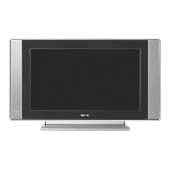
Page 2: Technical Specifications, Connections, And Chassis Overview
Specifications are indicative (subject to change). : ≈ 96 - Normal operation (W) - Stand-by (W) : < 1 Technical Specifications Dimensions (WxHxD cm) - 26PF5320/28 : 80.45 x 47.7 x 22.2 1.1.1 Vision - 32PF5320/28 : 92.4 x 55.0 x 22.2 Display type... - Page 3 Technical Specifications, Connections, and Chassis Overview LC4.3U AA EN 3 Cinch: Video CVBS - In, Audio - In PC VGA/DVI-2: Video 2fH RGB/YPbPr - In Ye - Video CVBS / 75 ohm Wh - Audio L 0.5 V / 10 kohm Rd - Audio R 0.5 V / 10 kohm...
- Page 4 EN 4 LC4.3U AA Technical Specifications, Connections, and Chassis Overview Chassis Overview LCD PANEL CLASS D AUDIO AMPLIFIER PANEL POWER SUPPLY SMALL SIGNAL BOARD PANEL KEYBOARD CONTROL PANEL SIDE I/O PANEL LED & IR PANEL F_15270_002.eps 2450505 Figure 1-5 Chassis overview...
-
Page 5: Safety Instructions, Warnings, And Notes
Safety Instructions, Warnings, and Notes LC4.3U AA EN 5 2. Safety Instructions, Warnings, and Notes Notes Index of this chapter: 2.1 Safety Instructions 2.2 Warnings 2.3.1 General 2.3 Notes • Measure the voltages and waveforms with regard to the Safety Instructions chassis (= tuner) ground (H), or hot ground (I), depending on the tested area of circuitry. - Page 6 For the repair of such sets nothing changes. Philips CE is producing lead-free sets (PBF) from 1.1.2005 onwards. In case of doubt whether the board is lead-free or not (or with...
-
Page 7: Directions For Use
Directions for Use LC4.3U AA EN 7 3. Directions for Use You can download this information from the following websites: http://www.philips.com/support http://www.p4c.philips.com... -
Page 8: Mechanical Instructions
EN 8 LC4.3U AA Mechanical Instructions 4. Mechanical Instructions Index of this chapter: Notes: 4.1 Cable Dressing • Figures below can deviate slightly from the actual situation, 4.2 Service Positions due to the different set executions. 4.3 Assy/Panel Removal • Follow the disassembling instructions in described order. - Page 9 Mechanical Instructions LC4.3U AA EN 9 The aluminium stands (order code 3122 785 90480) can be 4.3.3 LED Panel mounted with the back cover removed or still left on. So, the stand can be used to store products or to do measurements. It is also very suitable to perform duration tests without taking much space, without having the risk of overheating, or the risk of products falling.
- Page 10 EN 10 LC4.3U AA Mechanical Instructions 4.3.5 SSB Board Cover Shield (depending on model) 4.3.6 SSB Board F_15270_044.eps F_15270_073.eps 180505 260505 Figure 4-9 SSB board connectors Figure 4-7 Cable clip on cover shield F_15270_075.eps 260505 Figure 4-10 VGA connector screws 1.
- Page 11 Mechanical Instructions LC4.3U AA EN 11 4.3.7 Power Supply Panel (various models used) 4.3.8 Audio Amplifier Panel X530 X520 F_15270_049.eps 180505 Figure 4-12 Audio amplifier panel 1. Disconnect all cables (1) from the panel. 2. Remove the fixation screws (2) from the panel. 3.
- Page 12 EN 12 LC4.3U AA Mechanical Instructions 4.3.9 LCD Panel F_15390_047.eps 280205 F_15390_052.eps 280205 Figure 4-13 Anti-static copper foil Figure 4-16 Connectors X520 and X530 on power supply panel F_15270_051.eps 280205 F_15390_051.eps 280205 Figure 4-14 LVDS connector Figure 4-17 Connector 66B on LCD panel F_15390_050.eps 280205 Figure 4-18 LCD panel...
- Page 13 Mechanical Instructions LC4.3U AA EN 13 To remove the LCD-panel, carry out the following steps: Set Re-assembly 1. Cautiously pull back the upper parts of the anti-static copper foils next to the “L” and “R” loudspeakers (see To re-assemble the whole set, execute all processes in reverse Figure “Anti-static copper foil”).
-
Page 14: Service Modes, Error Codes, And Fault Finding
EN 14 LC4.3U AA Service Modes, Error Codes, and Fault Finding 5. Service Modes, Error Codes, and Fault Finding Index of this chapter: How to Enter 5.1 Test Points To enter SDM, use one of the following methods: 5.2 Service Modes •... - Page 15 Service Modes, Error Codes, and Fault Finding LC4.3U AA EN 15 How to Navigate Menu Explanation Use one of the following methods: 1. LLLLL. This represents the run timer. The run timer counts • When you press the MENU button on the remote control, normal operation hours, but does not count standby hours.
- Page 16 EN 16 LC4.3U AA Service Modes, Error Codes, and Fault Finding How to Store SAM Settings 8. Displays the detected Audio (e.g. stereo/mono). To store the settings changed in SAM mode, leave the top level 9. Displays the picture setting information. SAM menu by using the POWER button on the remote control 10.
- Page 17 UART SERVICE CONNECTOR CONNECTOR Service Tools 5.4.1 ComPair Introduction ComPair (Computer Aided Repair) is a service tool for Philips I 2 C Power Consumer Electronics products. ComPair is a further 9V DC development on the European DST (service remote control), E_06532_021.eps 180804 which allows faster and more accurate diagnostics.
- Page 18 EN 18 LC4.3U AA Service Modes, Error Codes, and Fault Finding How to Order • LVDS cable 41p-to-31p for CA1 (dual -> single LVDS): ComPair order codes (US): 3122 785 90830. • ComPair Software: ST4191. • ComPair Interface Box: 4822 727 21631. Error Codes •...
- Page 19 Service Modes, Error Codes, and Fault Finding LC4.3U AA EN 19 5.5.3 Error Codes The Blinking LED Procedure In case of non-intermittent faults, write down the errors present Using this procedure, you can make the contents of the error in the error buffer and clear the error buffer before you begin buffer visible via the front LED.
- Page 20 EN 20 LC4.3U AA Service Modes, Error Codes, and Fault Finding Table 5-3 NVM Default values (option bit settings through NVM Editor in SAM Mode) Byte Nr. Bit Feature/Mode Description Byte 0 0 QSS (LSB) Mode of quasi split sound amplifier 174(dec) 1 FMI Connection of output of QSS amplifier...
- Page 21 Service Modes, Error Codes, and Fault Finding LC4.3U AA EN 21 Byte Nr. Bit Feature/Mode Description Byte 5 0 FFI Fast Filter 179(dec) 1 NNR No red reduction during blue stretch 2 MUS NTSC matrix 3 GAM Gamma control 4 CBS Control sequence of beam current limiting 5 LLB Low level of beam current limiter...
- Page 22 EN 22 LC4.3U AA Service Modes, Error Codes, and Fault Finding 5.7.4 Video Processing 4. 24 V output (for inverter X520 & X530): Short-circuit proof with auto-restart. Over voltage protection when output voltage is more than 40% above nominal value. No Power 1.
-
Page 23: Block Diagrams, Testpoint Overviews, And Waveforms
Block Diagrams, Testpoint Overviews, and Waveforms LC4.3U AA 6. Block Diagrams, Testpoint Overviews, and Waveforms Wiring Diagram WIRING 8903 8903 INVERTER INVERTER INVERTER X220 POWER LVDS CONNECTION SUPPLY TO SCREEN LEFT RIGHT SPEAKER SPEAKER 1003 1001 8P06 CLASS D 8J03 AUDIO 1002 X200... -
Page 24: Block Diagram Video
Block Diagrams, Testpoint Overviews, and Waveforms LC4.3U AA Block Diagram Video VIDEO TUNER & VIF HERCULES MUX-SYNC INTERFACE SCALER FLASH/CONTROL EPLD +5SW_a 7217 7801 +VTUN TDA15021H GM1501 7C00 1102 1104 UV1318SD 7208 7E01 MX29LV040QC F624 1105 (Only for China) 2106 IF-TER VIF1 R_SDTV... -
Page 25: Block Diagram Audio
Block Diagrams, Testpoint Overviews, and Waveforms LC4.3U AA Block Diagram Audio AUDIO TUNER & IF HERCULES AUDIO PROCESSING AUDIO AMPLIFIER 7001 TDA8931T (CLASS-D) 7217 1102 1001 TDA15021H UV1318S(D) F108 2106 4110 1106 IF-TER SIF1 7004 RF IN IFOUT 4211 4618 QSS Mixer AUDOUTLSR AUDIO-R... -
Page 26: Testpoint Overview Small Signal Board
Block Diagrams, Testpoint Overviews, and Waveforms LC4.3U AA Testpoint Overview Small Signal Board F101 C1 F117 D2 F216 B3 F233 B3 F249 B2 F737 A3 F906 B6 FC10 B4 FD15 C7 FE13 C5 FG01 D4 FG17 D6 FG35 D3 FG53 D4 FJ13 A2 FK02 B1 FN02 A6... -
Page 27: I2C Ic Overview
Block Diagrams, Testpoint Overviews, and Waveforms LC4.3U AA I2C IC Overview I²C TUNER & IF COLUMBUS HERCULUS SCALER +3V3STBY +3V3SWB 7217 TDA15021H 7L07 7L06 HERCULES +3V3STBY PROCESSOR 7801 1102 7207 7M00 7L04 1101 M24C16 GM1501H UV1318S T6TU5XBG MST9883C +3V3SWB EEPROM SCALER TUNER COLUMBUS... -
Page 28: Supply Voltage Overview
Block Diagrams, Testpoint Overviews, and Waveforms LC4.3U AA Supply Voltage Overview SUPPLY LINE OVERVIEW TOP CONNECTORS TUNER & IF SCALER SIDE CONNECTORS MOJO SUPPLY PANEL (PSU) 5102 5K00 1540 1003 5103 5100 5K01 1304 HERCULES FLASH MEMORY 5J03 SCALER 5201 3265 7215 5900... -
Page 29: Circuit Diagrams And Pwb Layouts
Circuit Diagrams and PWB Layouts LC4.3U AA 7. Circuit Diagrams and PWB Layouts SSB: Tuner and VIF 1101 C1 F106 D2 1102 A1 F107 D3 TUNER & IF 1103 E2 F108 B4 1104 C9 F109 E5 1105 D8 F110 C10 1106 E9 F111 C10 1107 F3... -
Page 30: Ssb: Hercules (B2)
Circuit Diagrams and PWB Layouts LC4.3U AA SSB: Hercules 1201 B7 3215 B6 5209 D5 I216 C10 1202 G10 3216 A6 5210 D5 I217 C11 2201 A3 3217 B7 5211 E5 I218 D3 HERCULES 2202 B3 3218 B7 5212 E5 I219 C5 2203 D2 3219 B7... - Page 31 Circuit Diagrams and PWB Layouts LC4.3U AA SSB: Sync Interface 1440 D9 1441 E9 2447 E8 SYNC INTERFACE 2448 E9 2449 E4 3431 A3 3432 B3 3451 A5 3453 B6 3454 B7 3455 C6 3456 C7 3458 D2 +5VSW 3459 D4 +3V3STBY 4436 3461 E2...
- Page 32 Circuit Diagrams and PWB Layouts LC4.3U AA SSB: Audio Delay Line (Reserved) 2501 A2 2502 B2 AUDIO DELAY LINE (RESERVED) 2503 D2 2504 B8 2505 B9 2506 C10 2507 D10 2508 F6 2509 F7 F501 3501 F6 5501 1u0 +5VSWI +5VD 3502 F6 4501 E2...
-
Page 33: Ssb: Audio Processing (B5)
Circuit Diagrams and PWB Layouts LC4.3U AA SSB: Audio Processing AUDIO PROCESSING 2603 A5 I602 A8 2604 A6 I603 B8 FROM HERCULES 2605 B6 I604 A9 2608 B5 I605 B9 2609 B6 I606 C4 2610 B6 I607 C4 2611 B6 I608 A5 3605 4609... -
Page 34: Ssb: Dc-Dc Converter (B6)
Circuit Diagrams and PWB Layouts LC4.3U AA SSB: DC-DC Converter 1751 A10 7738 F2 2700 B11 7741 G3 DC-DC CONVERTER 2701 B11 7742 G4 2704 A3 7752 D9 2706 B3 7753 B10 2708 C3 7754 A9 2709 C3 7755 B8 2710 C2 7756 G8 FOR LCD ONLY... -
Page 35: Ssb: Diversity Tables B1-B6
Circuit Diagrams and PWB Layouts LC4.3U AA SSB: Diversity Tables B1-B6 TUNER & IF HERCULES SYNC INTERFACE AUDIO WITHOUT AMPLIFIER DC DC CONVERTER Item Description 2612 CER2 0603 Y5V 10V 1U COL Item Description Item Description 2613 CER2 0603 Y5V 10V 1U COL 2701 V V CER1 0402 NP0 50V 100P COL 1102... -
Page 36: Ssb: Scaler (B7)
Circuit Diagrams and PWB Layouts LC4.3U AA SSB: Scaler 1801 B12 7801-12 A4 SCALER 1802 G14 7801-4 C11 2800 A1 7801-5 E11 2801 A1 7801-6 F4 2802 A1 7801-9 G11 2803 A1 F800 A1 2804 A2 F801 B3 +3V3_PLL +2V5_DDR 2805 A2 F802 A9 F800... -
Page 37: Ssb: Scaler (B8)
Circuit Diagrams and PWB Layouts LC4.3U AA SSB: Scaler 2900 D1 F906 D10 2901 D2 F907 D10 SCALER 2902 D2 F908 E9 2903 E1 F909 E10 2904 E2 F910 G9 2905 A4 I900 C2 2906 A4 I901 E1 2907 A4 I902 E2 7801-14 2908 A4... -
Page 38: Ssb: Scaler Interface (B9)
Circuit Diagrams and PWB Layouts LC4.3U AA SSB: Scaler Interface 2A00 E3 SCALER INTERFACE 2A01 F2 2A02 F2 2A03 C7 2A12 F6 2A13 E8 3A00 E2 3A01 E2 7801-8 3A02 C5 GM1501-LF-BD 3A03 C6 3A04 C6 ACp|GPIO_G06_B6|DORED8 AE20 3A05 C6 ACn|GPIO_G06_B7|DORED9 AF20 TO SCALER... -
Page 39: Ssb: Sdram (B10)
Circuit Diagrams and PWB Layouts LC4.3U AA SSB: SDRAM 2B01 A1 SDRAM 2B02 A1 2B03 A1 2B04 A1 2B05 A2 2B06 A2 2B07 A2 +2V5_DDR 2B08 A3 2B09 A3 2B10 A3 2B11 A3 2B01 2B02 2B03 2B04 2B05 2B06 2B07 2B08 2B09 2B10... -
Page 40: Ssb: Flash / Control (B11)
Circuit Diagrams and PWB Layouts LC4.3U AA SSB: Flash / Control 1C00 E4 FLASH / CONTROL 2C00 A3 2C01 A3 2C02 E2 +3V3_IO 2C03 E5 3C00 E2 +3V3_IO 3C01 E5 3C02 E6 3C03 E6 3C04-1 A6 5C00 3C04-2 A6 TO SCALER 3C04-3 A6 2C00 TO SCALER... -
Page 41: Ssb: Hdmi (B12)
Circuit Diagrams and PWB Layouts LC4.3U AA SSB: HDMI 2D00 A3 2D06 F4 2D12 A5 2D18 B6 2D24 B7 2D30 B8 2D36 G11 2D44 F14 3D04 C2 3D10 C5 3D15-4 C11 3D17-2 D11 3D18-4 D11 3D21-4 F9 3D27 H13 3D35 H12 5D03 A7 7D04 E11 FD04 D2... -
Page 42: Ssb: Mux-Sync Interface (B13)
Circuit Diagrams and PWB Layouts LC4.3U AA SSB: MUX-Sync Interface 2E00 C2 3E50 C3 IE34 D10 MUX-SYNC INTERFACE 2E01 C2 3E51 C3 IE35 B7 2E02 C2 3E52 C3 IE36 B7 2E15 5E02 2E03 B5 3E53 D3 IE37 B7 IE08 +5VSWI 2E04 B7 3E54 D3 100n... -
Page 43: Ssb: Top Connectors (B16)
Circuit Diagrams and PWB Layouts LC4.3U AA SSB: Top Connectors 1J00 B1 FJ25 E7 1J01 C1 FJ26 E7 TOP CONNECTORS 1J02 D1 IJ01 B1 1J03 F1 IJ02 B1 1J04 B8 IJ03 B1 1J05 C8 IJ04 B1 1J06 E8 IJ05 B1 1J07 C2 IJ06 B1 1J08 C2... -
Page 44: Ssb: Side Connectors (B17)
Circuit Diagrams and PWB Layouts LC4.3U AA SSB: Side Connectors 1K00 A8 1K01 D1 SIDE CONNECTORS 1K02 E8 1K03 A1 1K04 D1 2K00 B7 2K01 B6 4K01 2K02 C3 FOR DISC/ ARCH CABINET TO/FROM 1540 OF 2K03 C3 4K03 IR/ LED RESERVED 1K03 1K00... -
Page 45: Ssb: Adc (B18)
Circuit Diagrams and PWB Layouts LC4.3U AA SSB: ADC 2L02 A7 3L37 E3 2L03 A7 3L38 C3 2L04 A7 3L39 C4 2L05 A8 4L00 D3 2L06 A8 4L01 D3 2L07 B7 4L02 C1 2L08 B7 4L03 C1 7L05 2L09 B7 4L04 C3 +3V3SWB +3V3SWB... -
Page 46: Ssb: Columbus (B19)
Circuit Diagrams and PWB Layouts LC4.3U AA SSB: Columbus 2M00 E2 3M87 A5 COLUMBUS 2M01 E2 3M88 C8 2M02 E3 3M89 C5 2M03 E3 3M90 E4 2M04 E3 4M00 B5 2M05 E3 4M01 B5 +3V3SWA +3V3SWA +3V3SWA 2M06 E3 4M02 B5 2M07 E3 4M03 B5 3M86... -
Page 47: Ssb: Epld (B20)
Circuit Diagrams and PWB Layouts LC4.3U AA SSB: EPLD 1N01 A9 7N02-2 D7 1N02 D11 7N02-5 D10 EPLD 1N03 F12 7N03-1 C3 1N05 D5 7N03-2 C2 2N01 A2 7N04 D5 2N02 C1 FN01 B4 2N03 C2 FN02 B6 +3V3-IO +3V3-IO +3V3-IO +3V3-IO +3V3-IO... - Page 48 Circuit Diagrams and PWB Layouts LC4.3U AA SSB: EPLD 1P01 E8 FP09 E4 1P02 E8 FP10 F4 1P03 F8 FP11 F4 EPLD 1P04 F8 FP12 F4 1P05 G8 FP13 F4 1P06 A11 FP14 G4 1P07 D11 FP15 D11 EAGLE INTERFACE 7N02-6 2P01 B3 FP16 D11...
-
Page 49: Ssb: Diversity Tables B9-B21
Circuit Diagrams and PWB Layouts LC4.3U AA SSB: Diversity Tables B9-B21 MUX-SYNC INTERFACE MUX-SYNC INTERFACE ANALOG I/O SCART SIDE CONNECTORS & PIXEL PLUS Item Description 2A00 CER2 0603 X7R 16V 100N COL Item Description 2A01 CER1 0402 NP0 50V 100P COL Item Description 1G01... -
Page 50: Ssb: Digital I/O (B22)
Circuit Diagrams and PWB Layouts LC4.3U AA SSB: Digital I/O 1Q01 A1 1Q03 E6 DIGITAL IO 2Q01 A4 2Q06 B4 2Q11 B4 2Q16 A2 2Q17 B1 2Q18 B2 AV3: VGA + 2fHYPbPr 2Q21 C5 TO PCHD-MUX 2Q23 D5 1Q01 5Q01 2Q25 D2 RINA|Pr FQ01... -
Page 51: Ssb: Cinch Analog I/O (1Fh)
Circuit Diagrams and PWB Layouts LC4.3U AA SSB: Cinch Analog I/O (1FH) 1R01 G14 3R98 J8 1R02-1 G1 4R01 F7 1R02-2 H1 4R02 E13 CINCH ANALOGUE IO (1FH) 1R02-3 H1 4R03 E13 1R03 I1 4R06 D3 1R06 E1 4R12 E4 1R07 A1 4R13 G8 2R00 F3... - Page 52 Circuit Diagrams and PWB Layouts LC4.3U AA Layout Small Signal Board (Top Side Overview) 1102 C6 1J04 A6 2203 A5 2230 B6 2248 B6 2269 A6 2448 A5 2716 A3 2903 C4 2D05 C1 2D38 C1 2E15 C4 2F08 D1 2G33 D3 2J02 A4 2J19 A5...
- Page 53 Circuit Diagrams and PWB Layouts LC4.3U AA Layout Small Signal Board (Top Side Part 1) Part 1 F_15270_034a.eps 180505...
- Page 54 Circuit Diagrams and PWB Layouts LC4.3U AA Layout Small Signal Board (Top Side Part 2) Part 2 F_15270_034b.eps 180505...
- Page 55 Circuit Diagrams and PWB Layouts LC4.3U AA Layout Small Signal Board (Top Side Part 3) Part 3 F_15270_034c.eps 180505...
- Page 56 Circuit Diagrams and PWB Layouts LC4.3U AA Layout Small Signal Board (Top Side Part 4) Part 4 F_15270_034d.eps 180505...
- Page 57 Circuit Diagrams and PWB Layouts LC4.3U AA Layout Small Signal Board (Bottom Side Overview) 1101 D2 2109 D1 2282 B3 2701 A6 2803 B6 2823 C5 2922 C6 2945 B6 2B07 B7 2D10 C7 2E25 C5 2G09 D4 2G52 D2 2K18 C1 2L18 B3 2N03 A6...
- Page 58 Circuit Diagrams and PWB Layouts LC4.3U AA Layout Small Signal Board (Bottom Side Part 1) Part 1 F_15270_035a.eps 180505...
- Page 59 Circuit Diagrams and PWB Layouts LC4.3U AA Layout Small Signal Board (Bottom Side Part 2) Part 2 F_15270_035b.eps 180505...
- Page 60 Circuit Diagrams and PWB Layouts LC4.3U AA Layout Small Signal Board (Bottom Side Part 3) Part 3 F_15270_035c.eps 180505...
- Page 61 Circuit Diagrams and PWB Layouts LC4.3U AA Layout Small Signal Board (Bottom Side Part 4) Part 4 F_15270_035d.eps 180505...
-
Page 62: Class D Audio Amplifier
Circuit Diagrams and PWB Layouts LC4.3U AA Class D Audio Amplifier 1001 E11 5001 A3 1002 C2 5002 C3 CLASS D AUDIO AMPLIFIER 1003 A2 5003 C2 2001 B2 5004 B3 2002 B3 5005 D3 2003 B3 5006 C8 2004 B4 5007 F8 POWER LINE FILTER HVPI-L... - Page 63 Circuit Diagrams and PWB Layouts LC4.3U AA Layout Class D Audio Amplifier (Top Side) 1001 A2 1003 A3 2004 A3 2019 A4 2024 A4 2037 A1 2043 A2 5007 A2 1002 A3 2001 A2 2012 A4 2023 A3 2029 A1 2042 A2 5006 A3 F_15390_023.eps...
-
Page 64: Keyboard Control Panel
Circuit Diagrams and PWB Layouts LC4.3U AA Keyboard Control Panel Personal Notes: 1008 D1 KEYBOARD CONTROL 1309 D2 1310 D2 1311 D3 1312 D3 1313 D3 1314 D2 1684 C1 3317 C1 3318 C2 3319 C2 3320 C3 3321 C3 3322 D3 HERCULES OTHERS 3323 D3... - Page 65 Circuit Diagrams and PWB Layouts LC4.3U AA Layout Keyboard Control Panel (Top Side) 1309 A1 1310 A3 1311 A5 1312 A7 1313 A8 1314 A4 1684 A1 F_15390_032.eps 3139 123 5974.1 210605 Layout Keyboard Control Panel (Bottom Side) 3317 A7 3318 A7 3319 A7 3320 A4...
-
Page 66: Side A/V Panel
Circuit Diagrams and PWB Layouts LC4.3U AA Side A/V Panel 1301 A1 1302-1 B1 SIDE-I/O 1302-2 C1 1302-3 D1 3302 1303 E1 1304 C8 2301 2302 2301 A4 2302 A4 SVHS 2303 A4 1301 2304 A4 I301 2305 C2 2306 D3 I303 3303 2307 D3... - Page 67 Circuit Diagrams and PWB Layouts LC4.3U AA Layout Side A/V Panel (Top Side) 1301 A1 1302 A3 1303 A4 1304 A2 9390 A3 9391 A2 9392 A2 9393 A3 F_15390_028.eps 3139 123 5956.1 280205 Layout Side A/V Panel (Bottom Side) 2301 A3 2302 A3 2303 A3...
-
Page 68: Ir-Led And Light Sensor Panel
Circuit Diagrams and PWB Layouts LC4.3U AA IR-LED and Light Sensor Panel Layout IR-LED and Light Sensor Panel (Top Side) 1870 B1 3801 B2 3808 E2 4807 E3 6803 C3 7804 C4 F802 C1 F806 B1 I804 C4 I810 D4 1870 A1 6801 A1 7802 A1... -
Page 69: Alignments
Alignments LC4.3U AA EN 69 8. Alignments Index of this chapter: 8.1 General Alignment Conditions 8.2 Hardware Alignments 8.3 Software Alignments Note: Figures below can deviate slightly from the actual situation, due to the different set executions. General: The Service Default Mode (SDM) and Service Alignment Mode (SAM) are described in chapter 5. - Page 70 EN 70 LC4.3U AA Alignments 8.3.1 SAM Menu 00035 LC4XUP1 1.08/S4XGVX 1.10 ERR 0 0 0 0 0 OP 000 057 140 032 120 128 000 . OP1 . Delta Cool Red . OP2 . Delta Cool Green -1 . OP3 .
- Page 71 Alignments LC4.3U AA EN 71 8.3.4 ADC Gain, Grey Scale Alignment & Panel Size Settings Caution: • Do not change the NVM settings without understanding the function of each setting, because The table below shows a number of NVM settings used for incorrect NVM settings may seriously hamper the each model of TV set.
- Page 72 EN 72 LC4.3U AA Alignments 8.3.5 Sound the Table “ADC Gain, Grey scale alignment & panel size settings” elsewhere in this manual. • For NICAM sets: see paragraph 8.3.3. • For other sets: No adjustments needed for sound. 8.3.6 Options Options OP1...OP7 in the SAM menu can be used for quickly restoring 64 features or settings of the HERCULES part of the TV set to their orginal default factory values (8 groups of 8...
- Page 73 Alignments LC4.3U AA EN 73 Table 8-3 Option codes in detail, at bit level Option byte & bit table for restoring the TV set to its original Factory Default settings via the NVM Editor in the SAM menu Description of feature/option to be switched ON or OFF bit 7 (msb) OP_PHILIPS_TUNER bit 6...
-
Page 74: Circuit Descriptions, Abbreviation List, And Ic Data Sheets
EN 74 LC4.3U AA Circuit Descriptions, Abbreviation List, and IC Data Sheets 9. Circuit Descriptions, Abbreviation List, and IC Data Sheets Index of this chapter: in this manual) and Crystal Clear. The block diagram below 9.1 Introduction (Figure 2.1) shows the Pixel Plus architecture; the 9.2 Block Diagram architectures of the other models are shown in the block 9.3 Input/Output... - Page 75 EN 75 Table 9-1 Models and picture quality Tuner and IF Model Picture quality A Philips UV1338 Tuner is used in the TV board. The SIF signals are decoded by the Hercules. Tuning is done via I N.A. Pixel Plus 32PF5320/28 Digital Crystal Clear 9.4.1...
- Page 76 EN 76 LC4.3U AA Circuit Descriptions, Abbreviation List, and IC Data Sheets Video: TV Part (Diagrams B1, B2, and B3) Figure 9-3 Block diagram video processing...
- Page 77 Circuit Descriptions, Abbreviation List, and IC Data Sheets LC4.3U AA EN 77 The video processing is completely handled by the Hercules Comb filter. Such a signal must be bypassed. Notch mode • IF demodulator. is not even an option since e.g. in double window, one part •...
- Page 78 EN 78 LC4.3U AA Circuit Descriptions, Abbreviation List, and IC Data Sheets about a “Field Comb Filter”. Field Comb filters are only for PAL The offset block receives the motion dependant 2D/3D Comb of commercial interest. filtered signal as input. The black level of the luminance signal Field Comb filters show also problems on vertical colour is restored and the result is output.
- Page 79 Circuit Descriptions, Abbreviation List, and IC Data Sheets LC4.3U AA EN 79 9.6.3 Noise Reduction and Noise Estimator Video: Scaler Part (Diagram B7, B8 and B9) The noise reduction function is a sophisticated successor of the The Genesis gm1501 Scaler is a dual channel graphics and noise reduction module from the PICNIC-chip, also known as video processing IC for LCD monitors and televisions “LIMERIC”.
- Page 80 EN 80 LC4.3U AA Circuit Descriptions, Abbreviation List, and IC Data Sheets 9.7.1 Teletext Path Audio Processing In Pixel Plus and Digital Crystal Clear models, which have an Hercules ADC (B18) and Columbus 3D combfilter (B19), the digital input of the scaler is used for the digital video signal (Columbus AUDIO-LSL 2x Stereo output), whereas the analogue RGB input input of the scaler is...
- Page 81 106 P0.0/ I2SDI/O Lip Sync I2SDI/O Monitor Controller. 107 P1.3/ T1 PC-TV_LED P1.3 • On-chip 80C51 micro-controller from Philips Semiconductor UOCIII (Hercules) series. 108 P1.6/ SCL Each micro-controller has it own I C bus which hosts its own 109 P1.7/ SDA internal devices.
-
Page 82: Abbreviation List
EN 82 LC4.3U AA Circuit Descriptions, Abbreviation List, and IC Data Sheets • LED. This signal is used as an indication for the Standby, 9.10 Abbreviation List Remote and Error Indicator. Region diversity: – During protection mode, the LED blinks and the set is 0/6/12 SCART switch control signal on A/V in standby mode. - Page 83 (Y/C) are reproduced LATAM LATin AMerica RGBHV Red, Green, Blue, Horizontal sync, LC04 Philips chassis name for LCD TV 2004 and Vertical sync Read Only Memory project Liquid Crystal Display Service Alignment Mode Light Emitting Diode; A semiconductor...
- Page 84 Sound right SCART1 out SNDR-SC2-IN Sound right SCART2 out SNDR-SC2-OUT Sound right SCART2 out SOPS Self Oscillating Power Supply S/PDIF Sony Philips Digital InterFace; This is a consumer interface used to transfer digital audio SRAM Static RAM STBY STandBY SVHS...
-
Page 85: Ic Data Sheets
Circuit Descriptions, Abbreviation List, and IC Data Sheets LC4.3U AA EN 85 9.11 IC Data Sheets This section shows the internal block diagrams and pin layouts of ICs that are drawn as "black boxes" in the electrical diagrams (with the exception of "memory" and "logic" ICs). 9.11.1 Diagram B2, Type TDA15021H (IC7217, Hercules) Block Diagram A “... - Page 86 EN 86 LC4.3U AA Circuit Descriptions, Abbreviation List, and IC Data Sheets 9.11.2 Diagram B19, Type T6TU5XB (IC7M00, Columbus) Figure 1 Package outline (top view) WEB/ UVA0 UVA2 UVA4 UVA6 UVA8 SEL656 TST1 HREF DAVB /Di0 /Di2 /Di4 /Di6 /Di8 UVA1 UVA3 UVA5...
- Page 87 Circuit Descriptions, Abbreviation List, and IC Data Sheets LC4.3U AA EN 87 9.11.3 Diagram B7+B8+B9, Type GM1501 (IC7401, Genesis) Block Diagram Parallel 2-wire IF/external Serial I/F JTAG GPIO micro Infra-red Rx Pulse Width Interface X186 External ndwid Modulator Micro- ROM I/F controller Internal Internal...
- Page 88 EN 88 LC4.3U AA Circuit Descriptions, Abbreviation List, and IC Data Sheets 9.11.4 Diagram B12, Type S9993CT (IC7D03, HDMI Panellink), Reserved Block Diagram RESET# CSDA Registers Slave CSCL DSDA ---------------- Configuration Slave DSCL Logic Block Aux Data Logic HDCP HDCP Block MCLK Keys...
-
Page 89: Spare Parts List
2228 3198 035 71040 100nF 10% 16V 0402 2812 3198 035 71040 100nF 10% 16V 0402 1150 3139 188 89951 ASSY SSB 26PF5320/28 2229 2020 552 96637 10µF 10% 6.3V 0805 2813 3198 035 71040 100nF 10% 16V 0402 1174 3139 188 89051 Audio Amp. - Page 90 EN 90 LC4.3U AA Spare Parts List 2B02 4822 124 11131 47µF 6.3V 2E34 2020 552 00005 4.7µF 10% 6.3V 0603 2M20 3198 035 71040 100nF 10% 16V 0402 2B03 3198 035 71040 100nF 10% 16V 0402 2E35 2020 552 00005 4.7µF 10% 6.3V 0603 2M21 2020 552 00183 2.2µF 10% 6.3V 0603 2B04...
- Page 91 Spare Parts List LC4.3U AA EN 91 3234 3198 031 04720 4.7kΩ 5% 0402 3829 4822 117 13606 10kΩ 5% 0.01W 0402 3E44 4822 117 13545 100Ω 1% 0402 3235 3198 031 04720 4.7kΩ 5% 0402 3831 4822 117 13545 100Ω 1% 0402 3E45 4822 117 13545 100Ω...
- Page 92 EN 92 LC4.3U AA Spare Parts List 3Q30 4822 051 30103 10kΩ 5% 0.062W 5208 4822 157 11716 Bead 30Ω at 100MHz 7214 9339 693 90135 BCP69-25 3Q31 4822 051 30103 10kΩ 5% 0.062W 5209 4822 157 11716 Bead 30Ω at 100MHz 7215 9339 693 90135 BCP69-25 3Q32...
- Page 93 Spare Parts List LC4.3U AA EN 93 2031 4822 126 14238 2.2nF 50V 0603 2032 4822 126 14238 2.2nF 50V 0603 Keyboard Control Panel [E] 2033 4822 126 13879 220nF +80-20% 16V 2034 2238 586 59812 100nF 20% 50V 0603 3801 4822 051 30332 3.3Ω...
-
Page 94: Revision List
EN 94 LC4.3U AA Revision List 11. Revision List Manual xxxx xxx xxxx.0 • First release. Manual xxxx xxx xxxx.1 • Latam region added. • HDMI (B12) schematic added. Manual xxxx xxx xxxx.2 • Spare Parts List added.