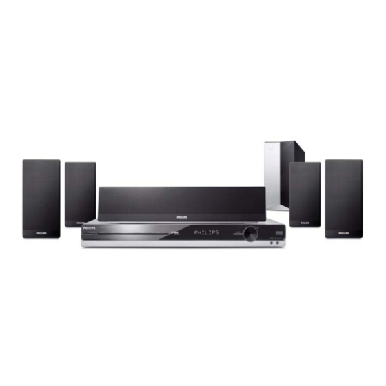
Philips HTR5205 Service Manual
Digital a/v surround receiver
Hide thumbs
Also See for HTR5205:
- Specifications (3 pages) ,
- User manual (27 pages) ,
- Quick start manual (2 pages)

Related Manuals for Philips HTR5205


Summary of Contents for Philips HTR5205
- Page 1 Digital A/V Surround Receiver HTR5205/ HTR5205/ Control & Vol & Phone Board 3139 785 32670...
- Page 2 LOCATION OF PCB BOARDS MAIN PCB TROL PCB POWER PCB VOL PCB PHONE PCB VERSION VARIATION: HTR5205 Type/Version Feature & Board in used Main PCB ( Power Output 600W) Power Voltage ( 120/230V ) Power cord(detachable)
- Page 3 Specifi cations AMPLIFIER Centre speaker System Full range satellite Total MAX Output Power Impedance: ................8 Ω Home Theater Mode: ............600W Speaker drivers: ..........x 2.5” woofer, Front: ................75 W x 2 ................1 x 2” tweeter ................../ Channel Frequency response: ........
- Page 4 Measurement Setup Tuner FM Bandpass Tuner AM (MW,LW) Bandpass...
- Page 5 SERVICE AIDS ESD Equipment: Service Tools: Anti-static table mat - large 1200x650x1.25mm ...4822 466 10953 Universal Torx driver holder .........4822 395 91019 anti-static table mat - small 600x650x1.25mm ..4822 466 10958 Torx bit T10 150mm ...........4822 395 50456 Anti-static wristband ..........4822 395 10223 Torx driver set T6-T20 .........4822 395 50145 Connectorbox (1M ..........4822 395 11307...
- Page 6 WAARSCHUWING WARNING Alle IC’s en vele andere halfgeleiders zijn All ICs and many other semi-conductors are gevoelig voor electrostatische ontladingen susceptible to electrostatic discharges (ESD). (ESD). Careless handling during repair can reduce life Onzorgvuldig behandelen tijdens reparatie kan drastically. de levensduur drastisch doen verminderen. When repairing, make sure that you are Zorg ervoor dat u tijdens reparatie via een connected with the same potential as the mass...
- Page 7 You will find this and more technical information • Use only lead-free solder alloy Philips SAC305 with within the “magazine”, chapter “workshop news”. order code 0622 149 00106. If lead-free solder-paste is required, please contact the manufacturer of your For additional questions please contact your local solder-equipment.
- Page 8 2 - 1 2 - 1 System , Region Code , etc. Setting Produre 1)System Reset a) switch source to DISC 6CH b) press and hold buttom on front panel c) VFD will display reset, then sysytem power down and return to original default setting 2)Version &...
- Page 9 2 - 2 2 - 2 REPAIR INSTRUCTION...
- Page 10 2 - 3 2 - 3 REPAIR INSTRUCTION...
- Page 11 3 - 1 3 - 1 Dismantling of the Main PCB DISASSEMBLY INSTRUCTIONS 1) Loosen 4 screw “ F “ on the top of main board as shown in fi gure 6. Dismantling of the top cover Assembly 2) Loosen 6 screw “ G ” at the back panel as shown in fi gure 7. 1) Loosen 5 screws to take out the Top Cover - 3 screws ”A”...
- Page 12 3 - 2 3 - 2 Service Position Dismantling of the Control Board 1) Loosen 13 screws “H” at the back pancle as shown in fi gure 8 Figure 8 Service A Dismantling of the Power Board 1) Loosen 5 screws “D” at the top of the Power Board as shown in fi gure 9 Service B Note:In some service positions the components or copper patterns of one board may risk touching its neighbouring pc boards or...
- Page 13 4 - 1 4 - 1 BLOCK DIAGRAM...
- Page 14 4 - 2 4 - 2 WIRING DIAGRAM VOL PCB CONTROL PCB PHOEN PCB MAIN PCB POWER PCB...
- Page 15 5 - 1 5 - 1 FTD DISPLAY PIN ASSIGNMENT CONTROL BOARD TABLE OF CONTENTS FTD Display Pin Assignment ............. 5-1 Voltage ....................5-2 Circuit Diagram( control pcb ) ............5-3 PCB Layout Top & Bottom View( control pcb ) ......... 5-4 Circuit Diagram( phone &...
- Page 16 5 - 2 5 - 2 VOLTAGE Q2051 Q2052 Pin NO Pin NO Voltage Voltage Pin NO Voltage -13.9 -27.1 -37.1 -16.4 Pin NO Voltage -18.5 -18.5 -27.1 -27.1 -14.1 -25.1 -23.1 -25.3 -25.3 -25.3 Pin NO Voltage...
- Page 17 5 - 3 5 - 3 CIRCUIT DIAGRAM (control pcb ) C2501 C2509 C2515 C2529 C2541 D2509 LD2501 A2 R2504 R2510 R2516 R2522 R2529 R2540 RB201 A1 TA2503 C1 TA2509 C1 ZD255 A1 C2502 C2510 C2516 C2530 D2501 DP2501 A3 Q2501 A2 R2505 R2511...
- Page 18 5 - 4 5 - 4 PCB LAYOUT - TOP VIEW ( control pcb ) D2501 LD2501 A1 TA2506 A1 JMP10 A2 JMP8 TA2507 A2 D2507 JMP11 A3 JMP15 A3 JMP19 A3 TA2501 A3 JMP21 A4 JMP25 A4 R2502 R2539 SN251 A4 JMP2 R2253...
- Page 19 5 - 5 5 - 5 PCB LAYOUT - TOP VIEW ( phone&vol pcb ) CIRCUIT DIAGRAM (phone & vol pcb) C2533 C2 C322 C4512 CN904 C2 FB4501 A1 JK303 VR2501 C2 C2533 C322 C4512 CN904 A1 FB4501 B1 JK303 C2534 C4510 C4513...
- Page 20 6 - 1 6 - 1 INTERNAL IC DIAGRAM - ES8380FAC Motor DVD/CD Motor Driver MAIN BOARD Video TV Display Audio Speakers SDRAM Audio Microphone In ES8380 (8/16-MB) Phoenix S/P DIF A/V Receiver EEPROM VFD Panel VFD Driver TABLE OF CONTENTS ROM/Flash Internal IC Diagram ................
- Page 21 6 - 2 6 - 2 Circuit Diagram(AMP pcb) C101 C4301 C2 C5233 B3 C5519 D3 L406 R4206 C2 R5202 B3 C102 C4302 C2 C525 C5520 D3 L407 R4207 C2 R5203 B3 C104 C4303 C2 C526 C5521 D3 L5201 B3 R4208 C2 R5204 B3 C105...
- Page 22 6 - 3 6 - 3 Circuit Diagram(main pcb) C0201 C1 C2079 B4 C278 FB302 D3 R2055 B3 R268 C0202 C1 C208 C279 FB303 D3 R2057 B3 R269 C0204 D4 C2080 B4 C280 FB304 D3 R2058 B3 R270 C0205 D4 C2081 B4 C281 FB305 D3...
- Page 23 6 - 4 6 - 4 PCB Layout Top View C0204 A2 C235 A3 C4105 C1 C5222 C1 FB203 B4 L213 R222 B3 R369 C2 R470 B1 C101 C4 C236 A3 C4106 A2 C5227 C1 FB204 B4 L215 R223 A3 R370 C2 R471 B1 C102 C4...
- Page 24 6 - 5 6 - 5 PCB Layout Bottom View C0201 C288 C567 R4307 C0202 C308 C568 R4407 C0205 C309 D2001 R450 C0207 C349 D2002 R4507 C0270 C359 D2003 R453 C0271 C360 D5006 R454 C122 C371 D5007 R5004 C123 C372 D5008 R5005 C124...
- Page 25 6 - 6 6 - 6 Voltage Pin NO Pin NO Voltage 0.02 0.03 0.01 -10.5 0.04 0.05 0.07 12.5 Voltage -23.8 23.6 23.7 -23.5 11.3 -11.9 -23.7 -23.8 Pin NO Voltage 11.2 -23.8 Pin NO Voltage 2.03 2.61 2.02 2.01 2.06 2.05...
-
Page 26: Voltage
7 - 1 7 - 1 VOLTAGE Pin NO Voltage Pin NO Voltage Pin NO Voltage Pin NO Voltage POWER BOARD Pin NO Voltage Pin NO Voltage Q901 Q902 Q903 Q904 Pin NO Pin NO Pin NO Pin NO Voltage Voltage Voltage 1.85... -
Page 27: Circuit Diagram
7 - 2 7 - 2 CIRCUIT DIAGRAM BD901 A1 C913 C925 C938 C951 C963 C977 D908 D921 IC905 Q904 Q916 R911 R923 R934 R946 R959 R971 R983 T902 ZD908 B4 C901 C914 C926 C939 C952 C964 C978 D909 D922 L901 Q905 Q917... -
Page 28: Pcb Layout Top View
7 - 3 7 - 3 PCB LAYOUT - TOP VIEW BD901 C920 C943 C954 C964 C976 D904 D922 IC903 J910 J920 J928 L901 Q901 Q912 R906 R937 R949 R979 TVR901 A1 C901 C921 C944 C955 C965 C977 D912 D923 IC904 J911 J921... -
Page 29: Pcb Layout Bottom View
7 - 4 7 - 4 PCB LAYOUT - BOTTOM VIEW C906 R927D A1 R902 D908 R913 R926A B1 R944 ZD912 B1 D901 R925 C909 C978 R981 C942 R967 R952 C907 C908 R929 D909 R914 R926B B1 R946 C924 D910 R955 C925 D916... - Page 30 9 - 1 9 - 1 Mechanical Exploded View...
- Page 31 9 - 2 9 - 2 MECHANICAL PART LIST Loc. Part No. Description 996510003624 DISPLAY LENS 996510001609 VOL RING 996510001610 VOL KNOB 996510001611 FRONT CAB 996510001612 SOURCE BUTTON SCREW HOLDER 996500036124 RUBBER FOOT 996500042571 FAN COVER 996510001690 TUNER PACK 996510001616 FUNCTION BUTTON 996510001617 STANDBY LENS...