Table of Contents
Advertisement
Quick Links
Download this manual
See also:
User Manual
Advertisement
Chapters
Table of Contents

Related Manuals for Philips HTR5204/12


Summary of Contents for Philips HTR5204/12
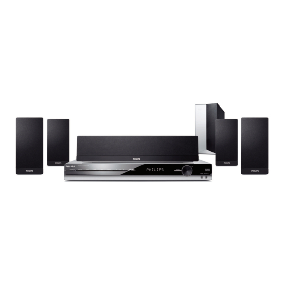
- Page 1 Digital A/V Surround Receiver HTR5204/ Control & Vol & Phone Board 313 9785 32660...
- Page 2 LOCATION OF PCB BOARDS MAIN PCB ROL PCB POWER PCB VOL PCB PHONE PCB VERSION VARIATION: HTR5200 Type/Version Feature & Board in used Main PCB ( Power Output 600W) Power Voltage ( 230V )
- Page 3 Sp ecifications CENTRE SPEAKER AMPLIFIER System Full range satellite Total MAX Output Power Impedance: 8 Ω Home Theater Mode: 600W Speaker drivers: 2 x 2.5” woofer, Front: 75W x 2 / Channel 1 x 2” tweeter Centre: 150W / Channel Frequency response: 150Hz –...
- Page 4 Measurement Setup Tuner FM Bandpass Tuner AM (MW,LW) Bandpass...
- Page 5 SERVICE AIDS Service Tools: Universal Torx driver holder .........4822 395 91019 Torx bit T10 150mm ...........4822 395 50456 Torx driver set T6-T20 .........4822 395 50145 Torx driver T10 extended ........4822 395 50423 Compact Disc: SBC426/426A Test disc 5 + 5A ......4822 397 30096 SBC442 Audio Burn-in test disc 1kHz ....4822 397 30155 SBC429 Audio Signals disc .........4822 397 30184 Dolby Pro-logic Test Disc ........4822 395 10216...
- Page 6 WAARSCHUWING WARNING Alle IC’s en vele andere halfgeleiders zijn All ICs and many other semi-conductors are gevoelig voor electrostatische ontladingen susceptible to electrostatic discharges (ESD). (ESD). Careless handling during repair can reduce life Onzorgvuldig behandelen tijdens reparatie kan drastically. de levensduur drastisch doen verminderen. When repairing, make sure that you are Zorg ervoor dat u tijdens reparatie via een connected with the same potential as the mass...
- Page 7 Due to lead-free technology some rules have to be Philips-sets respected by the workshop during a repair: You will find this and more technical information Use only lead-free solder alloy Philips SAC305 with • within the “magazine”, chapter “workshop news”. order code 0622 149 00106. If lead-free solder-paste...
- Page 8 2 - 1 2 - 1 System , Region Code , etc. Setting Produre 1)System Reset a) switch source to DISC 6CH b) press and hold buttom on front panel c) VFD will display reset, then sysytem power down and return to original default setting 2)Version &...
- Page 9 2 - 2 2 - 2 REPAIR INSTRUCTION...
- Page 10 2 - 3 2 - 3 REPAIR INSTRUCTION...
- Page 11 3 - 1 3 - 1 Dismantling of the Main PCB DISASSEMBLY INSTRUCTIONS 1) Loosen 4 screw “ F “ on the top of main board as shown in fi gure 6. Dismantling of the top cover Assembly 2) Loosen 5 screw “G” at the back panel as shown in fi gure 7. 1) Loosen 5 screws and remove the Top Cover by lifting the rear portion upwards before sliding it out towards the rear.
- Page 12 3 - 2 3 - 2 Service Position Dismantling of the Control Board 1) Loosen 11 screws “H” at the back pancle as shown in fi gure 8 Figure 8 Service A Dismantling of the Power Board 1) Loosen 4 screws “D” at the top of the Power Board as shown in fi gure 9 Service B Note:In some service positions the components or copper patterns of one board may risk touching its neighbouring pc boards or...
- Page 13 4 - 1 4 - 1 BLOCK DIAGRAM...
- Page 14 4 - 2 4 - 2 WIRING DIAGRAM VOL PCB CONTROL PCB PHOEN PCB MAIN PCB POWER PCB...
- Page 15 5 - 1 5 - 1 FTD DISPLAY PIN ASSIGNMENT CONTROL BOARD TABLE OF CONTENTS FTD Display Pin Assignment ............. 5-1 Voltage ....................5-2 Circuit Diagram( control pcb ) ............5-3 PCB Layout Top & Bottom View( control pcb ) ......... 5-4 Circuit Diagram( phone &...
- Page 16 5 - 2 5 - 2 VOLTAGE Q2051 Q2052 Pin NO Pin NO Voltage Voltage Pin NO Voltage -13.9 -27.1 -37.1 -16.4 Pin NO Voltage -18.5 -18.5 -27.1 -27.1 -14.1 -25.1 -23.1 -25.3 -25.3 -25.3 Pin NO Voltage...
- Page 17 5 - 3 5 - 3 CIRCUIT DIAGRAM (control pcb ) C2501 C2509 C2515 C2529 C2541 D2509 LD2501 A2 R2504 R2510 R2516 R2522 R2529 R2540 RB201 A1 TA2503 C1 TA2509 C1 ZD255 A1 C2502 C2510 C2516 C2530 D2501 DP2501 A3 Q2501 A2 R2505 R2511...
- Page 18 5 - 4 5 - 4 PCB LAYOUT - TOP VIEW ( control pcb ) D2501 LD2501 A1 TA2506 A1 JMP10 A2 JMP8 TA2507 A2 D2507 JMP11 A3 JMP15 A3 JMP19 A3 TA2501 A3 JMP21 A4 JMP25 A4 R2502 R2539 SN251 A4 JMP2 R2253...
- Page 19 5 - 5 5 - 5 PCB LAYOUT - TOP VIEW ( phone&vol pcb ) CIRCUIT DIAGRAM (phone & vol pcb) C2533 C2 C322 C4512 CN904 C2 FB4501 A1 JK303 VR2501 C2 C2533 C322 C4512 CN904 A1 FB4501 B1 JK303 C2534 C4510 C4513...
-
Page 20: Table Of Contents
6 - 1 6 - 1 INTERNAL IC DIAGRAM - ES8380FAC Motor DVD/CD Motor Driver MAIN BOARD Video TV Display Audio Speakers SDRAM Audio Microphone In ES8380 (8/16-MB) Phoenix S/P DIF A/V Receiver EEPROM VFD Panel VFD Driver TABLE OF CONTENTS ROM/Flash Internal IC Diagram ................ -
Page 21: Circuit Diagram(Amp Board)
6 - 2 6 - 2 Circuit Diagram(AMP pcb) C101 A1 C4304 C2 C528 D2 C5524 D3 L5401 C3 R4207 C2 R520 B4 C102 A1 C4305 C2 C5301 C3 C5525 D3 L5402 C3 R4208 C2 R5201 B2 C104 A1 C4306 C1 C5302 C3 C5527 D3 L5501 D3... -
Page 22: Circuit Diagram(Mian Pcb)
6 - 3 6 - 3 Circuit Diagram(main pcb) C0201 C1 C2068 B4 C273 FB302 D3 R2033 D4 R264 C0202 C1 C207 C274 FB303 D3 R2034 D4 R265 C0204 D4 C2070 B4 C275 FB304 D3 R2035 D4 R267 C0205 D4 C2071 B4 C276 FB305 D3... -
Page 23: Pcb Layout Top View
6 - 4 6 - 4 PCB Layout Top View C4505 A1 C513 A2 C418 A3 C296 A4 R5308 B1 C336 B3 FB236 B4 R5203 C1 C528 C3 IC301 C4 C464 A1 C5514 A2 C419 A3 C297 A4 R5309 B1 C337 B3 FB307 B4 R5204 C1... -
Page 24: Pcb Layout Bottom View
6 - 5 6 - 5 PCB Layout Bottom View C0201 C359 FB213 R5306 C0202 C360 FB309 R5307 C0205 C371 IC218 R5406 C0207 C372 L205 R5407 C0270 C383 L212 R5506 C0271 C384 L214 R5507 C110 C4003 Q5001 ZD101 C111 C4103 Q5002 ZD104 C122... -
Page 25: Voltage
6 - 6 6 - 6 Voltage Pin NO Pin NO Voltage 0.02 0.03 0.01 -10.5 0.04 0.05 0.07 12.5 Voltage -23.8 23.6 23.7 -23.5 11.3 -11.9 -23.7 -23.8 Pin NO Voltage 11.2 -23.8 Pin NO Voltage 2.03 2.61 2.02 2.01 2.06 2.05... -
Page 26: Voltage
7 - 1 7 - 1 VOLTAGE Pin NO Voltage Pin NO Voltage Pin NO Voltage Pin NO Voltage POWER BOARD Pin NO Voltage Pin NO Voltage Q901 Q902 Q903 Q904 Pin NO Pin NO Pin NO Pin NO Voltage Voltage Voltage 1.85... -
Page 27: Circuit Diagram
7 - 2 7 - 2 CIRCUIT DIAGRAM BD901 A1 C912 C923 C934 C946 C958 C969 C2 CN906 C1 D914 D925 L903 Q906 C4 Q917 C4 R911 R922 R932 R943 R954 R966 R977 R988 C4 TVR903 B1 ZD911 C2 C901 C913 C924 C935... -
Page 28: Pcb Layout Top View
7 - 3 7 - 3 PCB LAYOUT - TOP VIEW BD901 A1 TVR902 A2 J906 J909 R903 D912 R941 C916 L902 GT902 C1 C977 R966 D923 Q916 C955 J934 C903 C962 J907 L903 R904 D913 R942 C933 Q904 NTC901 C1 D921 R969 D924... -
Page 29: Pcb Layout Bottom View
7 - 4 7 - 4 PCB LAYOUT - BOTTOM VIEW C906 R927D A1 R902 D908 R913 R926A B1 R944 ZD912 B1 D901 R925 C909 C978 R981 C942 R967 R952 C907 C908 R929 D909 R914 R926B B1 R946 C924 D910 R955 C925 D916... - Page 30 9 - 1 9 - 1 Mechanical Exploded View...
- Page 31 9 - 2 9 - 2 MECHANICAL PART LIST Loc. Part No. Description 996510001608 DISPLAY LENS 996510001609 VOL RING 996510001610 VOL KNOB 996510001611 FRONT CAB 996510001612 SOURCE BUTTON VFD FILTER PC SCREW HOLDER 996500036124 RUBBER FOOT 996500042571 996510001615 FAN COVER 996510001607 TUNER PACK 996510001616...