Table of Contents
Advertisement
Quick Links
SERVICE MANUAL
Ver 1.1 2004. 03
AUDIO POWER SPECIFICATIONS
POWER OUTPUT AND TOTAL HARMONIC DISTORTION
With 8-ohm loads, both channels driven from 100 – 10,000 Hz; rated 1.0
W per channel minimum RMS power, with no more than 10% total
harmonic distortion in AC operation.
CD player section
System:
Compact disc digital audio system
Laser diode properties:
Material: GaAlAs
Wavelength: 780 nm
Emission duration: Continuous
Laser output: Less than 44.6 µW
(This output is the value measured at a distance of
about 200 mm from the objective lens surface on
the optical pick-up block with 7 mm aperture.)
Frequency response:
+1
20 – 20,000 Hz
dB
–1.5
Wow and flutter:
Below measurable limit
Radio section
Frequency range:
FM: 87.5 – 108 MHz
AM: 530 – 1,710 kHz
Sony Corporation
9-877-554-02
2004C04-1
Personal Audio Company
© 2004. 03
Published by Sony Engineering Corporation
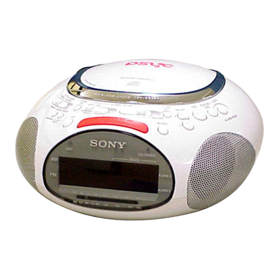
ICF-CD832
Model Name Using Similar Mechanism
CD
CD Mechanism Type
Section
Optical Pick-up Name
SPECIFICATIONS
General
Time display:
12-hour system
Speaker:
inches) dia., 8 Ω
66 mm (2
5 ⁄8
Power outputs:
1 W + 1 W (at 10% harmonic distortion)
Power requirements:
120 V AC, 60 Hz
Dimensions:
Approx. 229 × 104 × 218 mm (w/h/d)
(Approx. 9
× 4
1 ⁄8
projecting parts and controls
Mass:
Approx. 1,650 g (3 lb. 10 oz.)
Design and specifications are subject to change without
notice.
FM/AM CD CLOCK RADIO
US Model
Canadian Model
ICF-CD831
KSM-213RDP
KSS-213R
× 8
inches) incl.
1 ⁄8
5 ⁄8
1
Advertisement
Table of Contents

Related Manuals for Sony ICF-CD832


Summary of Contents for Sony ICF-CD832
- Page 1 Design and specifications are subject to change without Frequency range: notice. FM: 87.5 – 108 MHz AM: 530 – 1,710 kHz FM/AM CD CLOCK RADIO Sony Corporation 9-877-554-02 2004C04-1 Personal Audio Company © 2004. 03 Published by Sony Engineering Corporation...
- Page 2 REPLACE THESE COMPONENTS WITH SONY PARTS WHOSE NE REMPLACER CES COMPOSANTS QUE PAR DES PIÈCES PART NUMBERS APPEAR AS SHOWN IN THIS MANUAL OR SONY DONT LES NUMÉROS SONT DONNÉS DANS CE MANUEL IN SUPPLEMENTS PUBLISHED BY SONY. OU DANS LES SUPPLÉMENTS PUBLIÉS PAR SONY.
-
Page 3: Table Of Contents
ICF-CD832 TABLE OF CONTENTS 1. SERVICING NOTES 1-1. Cord Dressing (Power Cord) ..........5 1-2. Pointer Alignment ............... 5 2. GENERAL ................6 3. DISASSEMBLY 3-1. Cabinet (Upper) Assy ............7 3-2. Lid (CD) ................8 3-3. Chassis Assy ................ 8 3-4. -
Page 4: Servicing Notes
ICF-CD832 SECTION 1 SERVICING NOTES LASER DIODE AND FOCUS SEARCH OPERATION CHUCK PLATE JIG ON REPAIRING CHECK 1. Turn ON the [POWER] button and press [CD] button to CD On repairing CD section, playing a disc without the lid (CD), use position. -
Page 5: Cord Dressing (Power Cord)
ICF-CD832 1-1. CORD DRESSING (POWER CORD) 1) Set the power cord as shown in the figure. power cord 1-2. POINTER ALIGNMENT 1 Turn this in the arrow direction chassis assy until stopped. 3 Align the notch on the boss of the knob (tune) with the direction of CV1. -
Page 6: General
ICF-CD832 SECTION 2 GENERAL This section is extracted from instruction manual. -
Page 7: Disassembly
ICF-CD832 SECTION 3 DISASSEMBLY • The equipment can be removed using the following procedure. 3-1. CABINET (UPPER) ASSY (Page 7) 3-3. CHASSIS ASSY 3-2. LID (CD) 3-5. KEY (A) BOARD, (Page 8) KEY (B) BOARD (Page 8) (Page 9) 3-6. -
Page 8: Lid (Cd)
ICF-CD832 3-2. LID (CD) 5 claws 7 CD lid sub assy cabinet (upper) sub assy 6 holder (CD) 3 screw (BV tapping (B3)) 2 damper 1 screw 4 two screws (BV tapping (B3)) (BV tapping (B3)) 3-3. CHASSIS ASSY 3 three screws... -
Page 9: Main Board, Drive Board
ICF-CD832 3-4. MAIN BOARD, DRIVE BOARD 1 CN601 6 DRIVE board chassis assy 9 MAIN board 3 Removal the solders. 8 CN501 5 Removal the solders. 7 five screws (P 3x10) 2 Removal the solders. 4 shield plate (main) 3-5. KEY (A) BOARD, KEY (B) BOARD... -
Page 10: Cd Mechanism Deck
ICF-CD832 3-6. CD MECHANISM DECK 4 CD cover 0 CD mechanism deck 6 Removal the solders. 7 Removal the solders. 8 CD board 1 two screws (PWH 2.6x10) 2 two screws (PWH 2.6x10) 9 CNP701 5 screw (BVTT 2x6) 3-7. OPTICAL PICK-UP... -
Page 11: Electrical Adjustments
ICF-CD832 SECTION 4 ELECTRICAL ADJUSTMENTS TUNER SECTION 0 dB = 1 µV AM IF ADJUSTMENT • AM Section Adjust for a maximum reading on level meter. Setting: BAND switch: AM 450 kHz VOLUME control: MIN AM RF signal AM FREQUENCY COVERAGE ADJUSTMENT... - Page 12 ICF-CD832 Adjustment Location: FM LEAD WIRE ANTENNA SP101 (SPEAKER) CT1,L1 ANT1 AM TRACKING ADJUSTMENT CN301 CT2,L2 FM TRACKING ADJUSTMENT RV301 BPF1 AM IF TUNING ADJUSTMENT FM IF CT4,L4 ADJUSTMENT CT3,L5 AM FREQUENCY FM FREQUENCY COVERAGE COVERAGE ADJUSTMENT ADJUSTMENT — MAIN BOARD (component side) —...
-
Page 13: Cd Section
ICF-CD832 CD SECTION CD section adjustments are done automatically in this set. In case of operation check, confirm that focus bias. FOCUS BIAS CHECK Test Point: 1. Connect the oscilloscope between IC701 pin 4 and pin qa (or TP (RF) and TP (VREF)). -
Page 14: Diagrams
ICF-CD832 SECTION 5 DIAGRAMS 5-1. CIRCUIT BOARDS LOCATION TRANSFORMER board CD board KEY (A) board DRIVE board MAIN board KEY (B) board... -
Page 15: Block Diagram - Cd Section
ICF-CD832 5-2. BLOCK DIAGRAM — CD SECTION — CD BOARD CNP702 LCHO INTERPOLATION SLICE ERROR MUTE DIGITAL FIN2 EFMIN LEVEL CORRECTION & FILTER CONTROL AUDIO CD ATTENUATION & RCHO DEEMPHASIS 1-bit DAC PH/BH FIN1 CLV,CAV RF AMP, CONTROL SYSTEM SERVO PROCESSOR,... -
Page 16: Block Diagram - Tuner Section
ICF-CD832 5-3. BLOCK DIAGRAM — TUNER SECTION — MAIN BOARD (1/2) CV1-4 CT4,L4 CV1-1 FREQUENCY CT1,L1 COVERAGE TRACKING VREG BAND SW VREG VREG AM ANT AM OSC LPF2 FM/AM FRONTEND IF AMP,DET AMRF IN ST/MO FM/AM T1 AM IFT LOUT... -
Page 17: Block Diagram - Main Section
ICF-CD832 5-4. BLOCK DIAGRAM — MAIN SECTION — MAIN BOARD (2/2) IC301 Q102 POWER AMP VR301 TU-L VOLUME IN AMP OUT AMP CN301 CN302 TU-R R-CH (Page 16) CN501 Q101 Q103 SP101 STBY IC401 R-CH SYSTEM CONTROL R-CH Q301 SP201... -
Page 18: Printed Wiring Board - Cd Section
ICF-CD832 Ver 1.1 5-5. PRINTED WIRING BOARD — CD SECTION — • Refer to page 14 for Circuit Boards Location. THIS NOTE IS COMMON FOR PRINTED WIRING BOARDS AND SCHEMATIC DIAGRAMS. (In addition to this, the necessary note is printed in each block.) Common Note on Schematic Diagrams: •... -
Page 19: Schematic Diagram - Cd Section
ICF-CD832 5-6. SCHEMATIC DIAGRAM — CD SECTION — • Refer to page 18 for Common Note on Schematic Diagrams and page 26 for IC Block Diagrams. C727 C726 C724 C725 C721 R717 C730 C720 R716 R728 R727 C722 R718 (Page 20) -
Page 20: Schematic Diagram - Main Section
ICF-CD832 5-7. SCHEMATIC DIAGRAM — MAIN SECTION — • Refer to page 18 for Common Note on Schematic Diagrams and page 26 for IC Block Diagrams. C201 C216 C217 C116 C117 IC B/D C101 ANT1 C459 D403 R467 C456 D404... -
Page 21: Printed Wiring Board - Main Section
ICF-CD832 5-8. PRINTED WIRING BOARD — MAIN SECTION — • Refer to page 14 for Circuit Boards Location and page 18 for Common Note on Printed Wiring Boards. (Page 25) POWER BOARD CH901 MAIN BOARD ANT1 • Semiconductor Location SP101 Lch SPEAKER Ref. -
Page 22: Schematic Diagram - Control, Display Section
ICF-CD832 5-9. SCHEMATIC DIAGRAM — CONTROL, DISPLAY SECTION — • Refer to page 18 for Common Note on Schematic Diagrams. R601 R603 R605 R609 Q515 R602 R604 R606 R608 R610 R612 R613 R519 Q517 R518 S606 S601 S602 S603 S604... -
Page 23: Printed Wiring Boards - Key Section
ICF-CD832 5-10. PRINTED WIRING BOARDS — KEY SECTION — • Refer to page 14 for Circuit Boards Location and page 18 for Common Note on Printed Wiring Boards. KEY (A) BOARD S601 OFF/x ALARM RESET S602 RADIO KEY (B) BOARD... -
Page 24: Printed Wiring Board - Drive Section
ICF-CD832 5-11. PRINTED WIRING BOARD — DRIVE SECTION — • Refer to page 14 for Circuit Boards Location and page 18 for Common Note on Printed Wiring Boards. (Page 21) • Semiconductor MAIN BOARD Location W401 Ref. No. Location Q501... -
Page 25: Printed Wiring Board - Transformer Section
ICF-CD832 5-12. PRINTED WIRING BOARD — TRANSFORMER SECTION — • Refer to page 14 for Circuit Boards Location and page 18 for Common Note on Printed Wiring Boards. TRANSFORMER BOARD AC IN C902 R902 CH901 D902 D901 MAIN BOARD JW902... -
Page 26: Ic Pin Description
ICF-CD832 5-13. IC PIN DESCRIPTION 5-14. IC BLOCK DIAGRAMS • IC401 uPD789477GC-A28-8BT (SYSTEM CONTROL) Pin No. Pin Name Pin Description IC701 LC78646E-E (CD Board) 1 to 29 — Note used (Open) 30 to 37 SEG7 to SEG0 LED segment driver signal output AVDD —... - Page 27 ICF-CD832 IC702 BA5826FP-E2 (CD Board) IC301 LA4627 (MAIN Board) SP– D.BUFF SL– D.BUFF LEVEL D.BUFF – SHIFT D.BUFF SPIN LEVEL SHIFT – FILTER SLIN THERMAL SHUT-DOWN MONITOR (SLIN) REG–B VREF REGO MUTE (FIN) DRIVER MUTE (TIN) LEVEL LEVEL SHIFT D.BUFF SHIFT D.BUFF...
-
Page 28: Exploded Views
ICF-CD832 Ver 1.1 SECTION 6 EXPLODED VIEWS NOTE: • The mechanical parts with no reference • Color Indication of Appearance Parts The components identified by mark 0 or dotted line with mark number in the exploded views are not supplied. -
Page 29: Cabinet (Lower) Section
ICF-CD832 Ver 1.1 6-2. CABINET (LOWER) SECTION not supplied not supplied T901 SP101 SP201 The components identified by Les composants identifiés par une mark 0 or dotted line with mark marque 0 sont critiques pour 0 are critical for safety. -
Page 30: Chassis Section
ICF-CD832 Ver 1.1 6-3. CHASSIS SECTION KSM-213RDP LED501 not supplied Ref. No. Part No. Description Remark Ref. No. Part No. Description Remark 3-923-736-01 COVER, CD 3-248-346-02 CHASSIS 3-046-853-01 RUBBER, VIBRATION PROOF * 115 A-3347-607-A KEY (A) BOARD, COMPLETE 3-046-853-11 RUBBER, VIBRATION PROOF... -
Page 31: Cd Mechanism Section
ICF-CD832 Ver 1.1 6-4. CD MECHANISM SECTION (KSM-213RDP) M701 M702 The components identified by Les composants identifiés par une mark 0 or dotted line with mark marque 0 sont critiques pour 0 are critical for safety. la sécurité. Replace only with part number Ne les remplacer que par une piéce... -
Page 32: Electrical Parts List
ICF-CD832 Ver 1.1 SECTION 7 ELECTRICAL PARTS LIST NOTE: • Due to standardization, replacements in • Items marked “*” are not stocked since The components identified by mark 0 or dotted line with mark the parts list may be different from the they are seldom required for routine service. - Page 33 ICF-CD832 Ver 1.1 DRIVE KEY (A) Ref. No. Part No. Description Remark Ref. No. Part No. Description Remark R717 1-216-821-11 METAL CHIP 1/10W R506 1-216-801-11 METAL CHIP 1/10W R718 1-216-821-11 METAL CHIP 1/10W R507 1-216-801-11 METAL CHIP 1/10W R719 1-216-809-11 METAL CHIP...
- Page 34 ICF-CD832 KEY (A) KEY (B) MAIN Ref. No. Part No. Description Remark Ref. No. Part No. Description Remark R628 1-216-837-11 METAL CHIP 1/10W A-3347-588-A MAIN BOARD, COMPLETE (BLACK) R629 1-216-837-11 METAL CHIP 1/10W A-4547-112-A MAIN BOARD, COMPLETE (WHITE) R630 1-216-837-11 METAL CHIP...
- Page 35 ICF-CD832 MAIN Ref. No. Part No. Description Remark Ref. No. Part No. Description Remark C123 1-164-227-11 CERAMIC CHIP 0.022uF C436 1-162-970-11 CERAMIC CHIP 0.01uF C201 1-162-927-11 CERAMIC CHIP 100PF C437 1-162-970-11 CERAMIC CHIP 0.01uF C203 1-117-863-11 CERAMIC CHIP 0.47uF 6.3V...
- Page 36 ICF-CD832 MAIN Ref. No. Part No. Description Remark Ref. No. Part No. Description Remark < DIODE > 1-216-821-11 METAL CHIP 1/10W 1-216-801-11 METAL CHIP 1/10W D301 8-719-911-19 DIODE 1SS119-25 1-216-797-11 METAL CHIP 1/10W D302 8-719-941-09 DIODE DAP202U 1-216-817-11 METAL CHIP...
- Page 37 ICF-CD832 MAIN TRANSFORMER Ref. No. Part No. Description Remark Ref. No. Part No. Description Remark R421 1-216-841-11 METAL CHIP 1/10W < SWITCH > R423 1-216-841-11 METAL CHIP 1/10W R425 1-216-841-11 METAL CHIP 1/10W 1-692-181-21 SWITCH, SLIDE (BAND) R426 1-216-833-11 METAL CHIP...
- Page 38 ICF-CD832 Ver 1.1 Ref. No. Part No. Description Remark MISCELLANEOUS *************** 1-452-899-11 MAGNET 0 56 1-790-757-11 CORD, POWER 1-824-018-11 CABLE, FLEXIBLE FLAT (14 CORE) 1-501-907-51 ANTENNA, FM WIRE 1-757-689-11 CABLE, FLEXIBLE FLAT (16 CORE) 0 151 8-820-161-02 OPTICAL PICK-UP KSS-213R/C2RP...
- Page 39 ICF-CD832 MEMO...
- Page 40 ICF-CD832 REVISION HISTORY Clicking the version allows you to jump to the revised page. Also, clicking the version at the upper on the revised page allows you to jump to the next revised page. Ver. Date Description of Revision 2004. 02 2004.