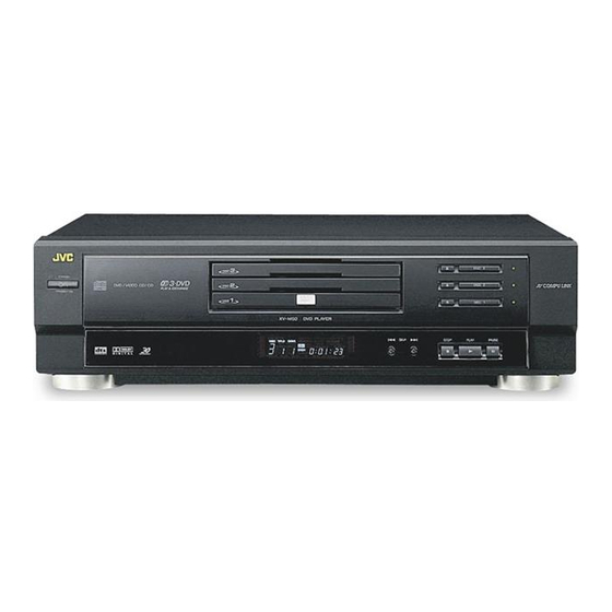
JVC XV-M50BK Service Manual
Hide thumbs
Also See for XV-M50BK:
- Service manual (87 pages) ,
- Instructions manual (52 pages) ,
- Service manual (88 pages)
Advertisement
Quick Links
SERVICE MANUAL
11
2002
A0008B
Because service manual XV-M50BK (Issue No.A0008)
which has already been issued contains some mistakes,
the following pages are modified in this service manual.
< Modified pages >
*Description of major ICs
*Block diagrams
Refer to the service manual XV-M50BK (Issue No. A0008)
which has already been issued for other pages.
1
Description of major ICs . . . . . . . . . . . . . . . . . . . . . . . . . . . . . . . . . . . . . . . . . . . . . . . . . . . . . . . . . . . . . . . . . 2
2
Block diagrams . . . . . . . . . . . . . . . . . . . . . . . . . . . . . . . . . . . . . . . . . . . . . . . . . . . . . . . . . . . . . . . . . . . . . . . . 29
DVD VIDEO PLAYER
XV-M50BK
Supplement
TABLE OF CONTENTS
COPYRIGHT © 2002 VICTOR COMPANY OF JAPAN, LTD.
XV-M50BK
Area Suffix
J ------------- U.S.A.
C ---------- Canada
No.A0008B
2002/11
Advertisement

Related Manuals for JVC XV-M50BK


Summary of Contents for JVC XV-M50BK
- Page 1 < Modified pages > *Description of major ICs *Block diagrams Refer to the service manual XV-M50BK (Issue No. A0008) which has already been issued for other pages. TABLE OF CONTENTS Description of major ICs ..............2 Block diagrams .
- Page 2 XV-M50BK SECTION 1 Description of major ICs 1.1 AK93C65AF-X (IC403) : EEPROM • Pin layout • Block diagram • Pin function Pin no. Symbol Function Program enable (With built-in pull-up resistor) Power supply Chip selection Cereal clock input Cereal data input...
- Page 3 XV-M50BK 1.2 AN8702FH(IC101):Frontend processor • Pin layout • Pin function Pin No. Symbol Description Input for Laser current monitor PC01 Laser power control output for DVD Photo detector fo CD PC02 Laser power control output for CD TGBAL Tangential phase balance control terminal...
- Page 4 XV-M50BK Pin No. Symbol Description DCRF All addition amplifier capacitor terminal OFTR OFTR output teminalr BDO output terminal RFENV RF envelope output terminal BTTOM Bottom envelope detection filter terminal PEAK Peak envelope detection filter terminal AGCG AGC amplifier gain control teminalr...
- Page 5 XV-M50BK 1.3 HY57V161610DTC8(IC504,IC505) : 16MB SDRAM • Block diagram • Pin function Pin No. Symbol Description Power supply DQ0,1 Data input/output Connect to GND DQ2,3 Data input/output Power supply DQ4,5 Data input/output Connect to GND 11,12 DQ6,7 Data input/output Power supply...
- Page 6 XV-M50BK 1.4 M35500AFP(IC802) : FL Driver • Pin layout • Pin function Pin No. Symbol Description Power supply terminal XOUT The short-circuit is made and the capacitor is connected with XIN on the outside Connect to ground The short-circuit is made and the capacitor is connected with XOUT on the outside...
- Page 7 XV-M50BK 1.5 M56788FP-W (IC271) : Traverse mechanism driver • Terminal Layout • Block diagram...
- Page 8 XV-M50BK 1.6 MN101C49GGJ1(IC701): System controller • Terminal layout • Pinfunction Pin No. Symbol Function Connect to ground No connect No connect No connect NTSEL NTSC/PAL selection POWER SW Power switch detect terminal SHUT1 Connect to VDD KEY1-5 Connect to VDD...
- Page 9 XV-M50BK Pin No. Symbol Function CHREQ Changer commnication REQUEST CHST Changer commnication STROBE CHDATA Changer commnication DATA I/O No connect CHCK Channel clock FLDATAO Serial data output FLDATAI Serial data input FLCK Clock output of serial transfer FLCS Chip select output...
- Page 10 XV-M50BK Pin No. Symbol Function No connect M1M3 No connect No connect No connect GAIN2 No connect GAIN1 No connect HPMUT No connect DAVSS No connect LMUTE No connect CMUTE No connect SMUTE No connect MUTE Muting control signal output...
- Page 11 XV-M50BK 1.7 MN102L62GGP (IC401) : Unit CPU PinNo. Symbol Function PinNo. Symbol Function Power supply WAIT Micon wait signal input FEPEN Serial enable signal for FEP Read enable SLEEP Standby signal for FEP SPMUTE Spindle muting output to IC251 BUSY...
- Page 12 XV-M50BK 1.8 MN103S13BDA(IC301):Optical disc controller • Pin layout • Block diagram...
- Page 13 XV-M50BK • Pin function PinNo. Symbol Description HDD15 I/O ATAPI Data HDD0 I/O ATAPI Data HDD14 I/O ATAPI Data Power supply 3V HDD1 I/O ATAPI Data HDD13 I/O ATAPI Data HDD2 I/O ATAPI Data Connect to GND HDD12 I/O ATAPI Data Power supply 2.7V...
- Page 14 XV-M50BK PinNo. Symbol Description CPUADR7 System control address CPUADR6 System control address CPUADR5 System control address CPUADR4 System control address CPUADR3 System control address CPUADR2 System control address CPUADR1 System control address Connect to GND CPUADR0 System control address System control chip select...
- Page 15 XV-M50BK PinNo. Symbol Description BLKCK Sub code/block/input clock LRCK Identification signal of L and R (Connect to VSS) Connect to GND OSCI1 Oscillation input terminal 16.9MHz OSCO1 Oscillation output terminal 16.9MHz Power supply 3V PVSS Connect to GND PVDD Power supply 3V...
- Page 16 XV-M50BK 1.9 MN35505-X (IC703) : DAC • Terminal layout • Pin function Pin No. Symbol Description Control signal for DAC Digital data input LRCK L and R clock for DAC Bit clock for DAC Control signal for DAC DVDD2 Power supply terminal...
- Page 17 XV-M50BK 1.10 MN67706ZY (IC201) : Auto digital servo controller • Terminal layout • Pin functions Pin No Symbol Function AS(AD2) AS :Full adder signal(FEP) TE(AD1) Phase difference/3 beam tracking error(FEP) FE(AD0) Focus error(FEP) AVDD Apply 3.3V(For analog circuit) FODRV(DA1) Focus drive(DRVIC)
- Page 18 XV-M50BK Pin No Symbol Function RFDIF Not use CSLFL1 I/O Pull-up to VHALF VFOSHORT VFO short output AVDD Apply 3.3V(For analog circuit) HPFIN Pull-up to VHALF HPFOUT Connect to TP208 AVSS Ground(For analog circuit) LPFIN Pull-up to VHALF LPFOUT Not use...
- Page 19 XV-M50BK Pin No Symbol Function MINTEST Pull-down to Ground(For MINTEST) TEST Pull-down to Ground(For TEST) 33VSS Ground(For I/O) 33VDD Apply 3.3V(For I/O) CHCK40 Clock for SRDATA(ODC) DAT3 SRDATA3(ODC) DAT2 SRDATA2(ODC) DAT1 SRDATA1(ODC) DAT0 SRDATA0(ODC) 33VSS Ground(For I/O) 33VDD Apply 3.3V(For I/O)
- Page 20 XV-M50BK 1.11 MR27V1602EN8MAX (IC402) :P2 ROM of 1,048,576word x 16 bit / 2,097,152 word x 8 bit • Pin layout • Block diagram • Pin functions Symbol Function A0 - A20 Address Input D0 - D14 Data Output Chip Enable...
- Page 21 XV-M50BK 1.12 TA8409S (IC802,IC803) : Motor driver • Pin layout • Pin function INPUT OUTPUT MODE OUT 1 OUT 2 MOTOR Infinity Infinity STOP CW/CCW CCW/CW BRAKE • Pin function Pin No. Symbol Description Input terminal Power supply terminal for logic...
- Page 22 XV-M50BK 1.13 TC74VHC00FT-X (IC503) : Write timing control • Terminal layout / Block diagram • Truth table 1.14 TC74VHC125FT-X (IC411) : Buffer • Terminal layout / Block diagram • Truth table INPUTS OUTPUTS X : Don’t care Y : High impedance 1.15 TC7WT125FU-X(IC412) : Dual bus buffer...
- Page 23 XV-M50BK 1.16 UPD65612GB-208(IC801):Changer control micon • Terminal layout • Pin function Pin No. Symbol I/O Function Pin No. Symbol I/O Function 2SSW I Switch input signal to TRAY2 - Non connect 1SSW I Switch input signal to TRAY1 - Non connect...
- Page 24 XV-M50BK 1.17 ZIVA-4.1-PB0(IC501) : Back end - Digital decoder • Terminal layout • Pin function Pin No. Symbol Description Read strobe input Read/write strobe input VDD_3.3 Power supply terminal 3.3V WAIT Transfer not complete / data acknowledge. Active LOW to indicate host initiated transfer is complete.
- Page 25 XV-M50BK Pin No. Symbol Description Non connect Non connect Non connect Non connect Non connect PIO0 I/O Programmable I/O terminal Connect to ground VDD_3.3 Power supply terminal 3.3V PIO1 I/O Programmable I/O terminal PIO2 I/O Programmable I/O terminal PIO3 I/O Programmable I/O terminal...
- Page 26 XV-M50BK Pin No. Symbol Description MADDR5 SDRAM address VDD_2.5 Power supply terminal 2.5V Connect to ground MADDR4 SDRAM address SDRAM write enable SD-CAS Active LOW SDRAM column address VDD_3.3 Power supply terminal 3.3V Connect to ground SD-RAS Active LOW SDRAM row address...
- Page 27 XV-M50BK Pin No. Symbol Description VDD_DAC Power supply terminal for analog video DAC VDD_VIDEO Power supply terminal for analog video Non connect VSS_DAC Connect to ground for analog video DAC VSS_VIDEO Connect to ground for analog video CVBS/G/Y DAC video output format. Macrovision encoded...
- Page 28 XV-M50BK Pin No. Symbol Description VDD_3.3 Power supply terminal 3.3V RESERVED Tie to VSS or VDD_3.3 as specified in table 1 VDD_3.3 Power supply terminal 3.3V Connect to ground Non connect RESERVED Tie to VSS or VDD_3.3 as specified in table 1...
- Page 29 XV-M50BK SECTION 2 Block diagrams 2.1 General view...
- Page 30 XV-M50BK 2.2 DVD Servo control section (SHEET 1,2) CN502 CN503 WAITODC CN101...
- Page 31 XV-M50BK 2.3 System control section (SHEET 3) J702 AVCI/O Q709 FLRST,STANDBY IND COMPULINK TO CN801 FLCK,FLDATAI/O SHEET 5 FLCS,REMO RESET RESET POWER SW TO CN951 IC702 SHEET 6 EEPROM IC791 P.ON X701 EEDI/O POWER SYSTEM +12V 10MHz EECS SUPPLY CONTROLLER...
- Page 32 XV-M50BK 2.5 Video signal output section (SHEET 4) C/R/V J601 L602 Y/B/U COMPONENT VIDEO OUT L612 TO CN503 SHEET 2 CVBS/G/Y L622 S-VIDEO OUT CVBS COMPOSITE L632 VIDEO OUT J602 2.6 Connection to pick-up section (SHEET 8) LASER SHORT SW...
- Page 33 XV-M50BK 2.8 Power supply section (SHEET 6) CN971 CN961 CN951/CN952...
- Page 34 XV-M50BK VICTOR COMPANY OF JAPAN, LIMITED AV & MULTI MEDIA COMPANY 1644, Shimotsuruma, Yamato, Kanagawa 242-8514, Japan (No.A0008B) Printed in Japan 2002/11...